Accelarated Publication
Evaluation of Cu-bumps with lead-free solders for flip-chip package applications
Kung-Liang Lin, Edward-Yi Chang
*, Lin-Chi Shih
Department of Materials Science and Engineering, National Chiao-Tung University, 1001 Ta-Hsueh Rd., Hsinchu 30010, Taiwan
a r t i c l e
i n f o
Article history:
Received 6 February 2009 Accepted 26 April 2009 Available online 6 May 2009 Keywords:
Copper bump Lead-free Electroplating
a b s t r a c t
Low cost electroplated Cu-bump with environmental friendly Sn solder was developed for flip-chip appli-cations. The seed layer used was Ti/WNx/Ti/Cu where WNxwas used as the Cu diffusion barrier and Ti was
used to enhance the adhesion between bump and the chip pad. Thick negative photoresist (THB JSR-151N) with a high aspect ratio of 2.4 was used for electroplating of copper bump and Sn solder. The Sn solder cap was reflowed at 225° for 6 min at N2atmosphere. No wetting phenomenon was observed
for the Sn solder as evaluated by energy-dispersed spectroscopy (EDS). The Cu-bump with Ti/WNx/Ti/Cu
seed layer not only have higher shear force than the Cu-bump with Ti/Cu seed layer but also has higher resistance to fatigue failure than the Au, SnCu, SnAg bumps.
Ó 2009 Elsevier B.V. All rights reserved.
1. Introduction
Flip-chip technology can dramatically reduce the packaging cost as compared to wire bonding for high frequency component assembly because their’s no need for individual chip tuning for package. This technology provides a chip bonding process which meets the requirements of small dimensions, thin packages, low cost, and high reliability[1]. For the solder balls used in flip-chip technology, SnAg and SnCu are the most promising materials to re-place the conventional SnPb solder which will be prohibited in the near future due to the toxicity of Pb. The European Union Waste in electrical and electronic equipment (WEEE) has proposed to ban Pb usage in electronic products by 2008[2]. For flip-chip interconnec-tions, bumps are required either on the substrate or on the chip side[3]. In high volume production, the bumps are usually formed either by photolithography combined with electroplating, or elec-troless deposition followed by solder printing. The development of advanced wireless communication system has increased the need of packaging applications at higher frequencies. For high frequency integrated circuits (RFIC), smaller bump cross section is required to improve the RF performance, however, the cross section is limited by the resolution and the aspect ratio of the photoresist used in the lithography. The bump shape also affects the performance [4], when the spacing between the chip and board is reduced, more field fringes into the substrate which will reduce the microwave line impedance. Simulations results show that when RFIC fre-quency is above 60 GHz, the bump height must be above 50
l
m to reduce the electromagnetic (EM) interference between the RFIC on the chip and the substrate[5].Low cost Cu-bump instead of Au bump with environment friendly lead-free Sn cap is developed with heights up to 85
l
m for microwave flip-chip packaging in this study. The copper bumps developed contain Ti/WNx/Ti/Cu diffusion barrier and are high en-ough (> to 50l
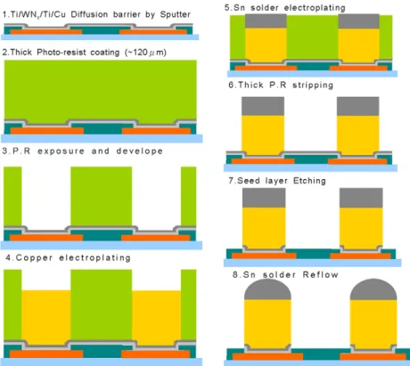
m) prevent the EM field fringe into the substrate and also to make the substrate surface less sensitive to the strains caused by the coefficient of thermal expansion (CTE) differences. 2. ExperimentalThe process flow of the flip-chip bumps in this study is shown in
Fig. 1. An under bump metallization (UBM) layer was first sput-tered on the bare 3 in. GaAs wafer substrate. The UBM consisted of sputtered Ti/WNx/Ti/Cu metallization layers from bottom to top and their thicknesses were 30/60/30/100 nm, respectively. These UBM layer was used as seed layer for subsequent electro-plating. The WNxlayer is an effective copper diffusion barrier layer
[6]. After the UBM layer metallization, a negative photoresist (JSR THB-151N) was spun on the wafer, as the plating mask, the thick-ness of the photoresist was 120
l
m and the diameter of the pat-terns was 50l
m. After the photoresist was patterned, copper bumps were electroplated using CuSO4 -based electrolyte solution with the current density of 3.5 ASD (A/dm2). Sn solder was electro plated on top of the Cu-bumps with SnSO4-based solution. In order to enhance the wettability of the resist surface to the electrolyte solution and to activate the metallic seed layer, the wafer was dipped in the acid-based copper electrolyte solution shortly before electroplating. After electroplating, the photoresist was removed by stripper solution (JSR THB-S1) at 65 °C, and the WNxand Ti lay-ers were removed by wet etch. The reflow of the solder material was performed at 225 °C for 6 min. The reflow temperature and time were optimized to achieve optimum Sn–Cu-bump composi-0167-9317/$ - see front matter Ó 2009 Elsevier B.V. All rights reserved.doi:10.1016/j.mee.2009.04.027
*Corresponding author. Tel.: +886 3 5131536; fax: +886 3 5751826. E-mail address:edc@mail.nctu.edu.tw(E.-Y. Chang).
Microelectronic Engineering 86 (2009) 2392–2395
Contents lists available atScienceDirect
Microelectronic Engineering
tions. The total height of the Cu-bump and the Sn solder was mea-sured by scanning electron microscopy (SEM). The shear strength of the bump was examined by commercial test apparatus (Dage-4000). The testing speed was 100
l
m/s, test load was 100 g, and the shear height was set at 10l
m from the bottom of the bump. The solder voids were examined by X-ray (SMX-160 E-II after the solder reflow. Sn solder wettability was characterized by energy-dispersed spectroscopy (EDS) mapping.3. Results and discussions
3.1. Copper bumps with plated Sn cap
Copper bumps were fabricated by electroplating process. The maximum aspect ratio achieved for the plated Cu-bumps using JSR THB-151N negative thick photoresist was up to 2.4. For thick photoresist coating, the resist thickness and uniformity mainly de-pend on the spin time and the spin speed. Non-uniform plating with partial filling of the plating via might occur during the elec-troplating process for the high aspect ratio photoresist. These prob-lems can be solved by adding additives, controlling flow rate and using pulsed current plating. The uniformity of the height of the plated copper bumps can be improved by controlling the plating current density, the electrolyte flow rate and the electrolyte solu-tion concentrasolu-tion[7]. In this study, the copper plating was per-formed using 3.5 ASD (A/dm2) current density, 10 l/min electrolyte flow rate and 1/100 s pulse current. Due to the current crowding in the wafer edge, the plated bump around the edge of the wafer was 2–4
l
m higher than the bumps at the wafer center. The copper bump with Ti/WNx/Ti/Cu UBM layer and the plated Sn solder on the top is as shown inFig. 2. The plated copper bumps had a height of 65–70l
m. The height of copper bump in the struc-ture is important in preventing of the EM interference between the chip and the lead-frame, it also determines the Sn solder thickness. Too thick plated solder could lead to solder bridging or solder spreading on the lead-frame at the reflow process. The Sn solderplated on the copper bumps was between 25–30
l
m in height, it provides a robust assembly process and the highest reliability[8]. 3.2. Bump shear strength test resultsFor the solders used in the flip-chip package, bonding strength of the solder to the UBM on chip side is very important. In order to evaluate the shear strength of the copper bumps on the UBM with Cu diffusion barrier, copper bumps on different UBM layers including Ti/Cu and Ti/WNx/Ti/Cu were tested and compared. Also the shear strength of different bump materials including Au, SnCu, Fig. 1. Schematic of the process flow for the fabrication of the Cu-bump with lead-free solder.
Fig. 2. SEM micrograph of the copper bump array with Sn cap. K.-L. Lin et al. / Microelectronic Engineering 86 (2009) 2392–2395 2393
SnAg bumps were compared in this study. The shear force was con-ducted using global bond test (Dage-4000s, Richardson Electronics Ltd.). Shear blade height was set at 10
l
m from the bottom of the bump. Shear force test results are shown inFig. 3with eachmate-rial tested for 60 samples. Only two types of failure modes were observed. The failure occured either inside the solder as shown in the insert picture inFig. 3or between the UBM and the wafer interface (not shown here). For the copper bumps on Ti/WNx/Ti/ Cu UBM, the failure mode was inside the solder and it has higher shear strength than the bumps with Ti/Cu UBM. For the bumps with Ti/Cu UBM, the failure mode was at the interface of UBM and wafer. It indicates that the Ti/WNx/Ti/Cu UBM can act as an effective Cu diffusion barrier and also provides a strong adhesion between the bump and the chip pad. The shear force of copper bumps is also stronger than Au, SnCu, SnAg bumps, this means that the copper bump fabricated by electroplating has acceptable mechanical properties for flip-chip package applications.
Fig. 3. Shear force test results for different types of bumps.
Fig. 4. SEM image of the Sn solder after reflow.
Fig. 5. X-ray image for the examination of the void in the solder after reflow.
Fig. 6. Energy-dispersed spectroscopy (EDS) mapping of the copper bump with Sn cap: (a) Sn element mapping, (b) Cu element mapping, and (c) SEM image. 2394 K.-L. Lin et al. / Microelectronic Engineering 86 (2009) 2392–2395
3.3. Sn soldering
After the electroplating process, resist was stripped and the Cu diffusion barrier layer beneath the resist was removed. The reflow process of the Sn solder was performed to form a solder ball on the top of the copper posts as shown inFig. 4. The Sn solder reflow pro-cess was performed using horizontal furnace at 225 °C for 6 min at N2 atmosphere to prevent the possible oxidation of the solder material. Oxidation on the surface of the solder material may effect the reliability of the solder joint to the substrate. No void or defect was found in the solder and the Cu-bump materials as analyzed by X-ray (SMX-160E-II) analysis. The X-ray mapping data after solder-ing is shown inFig. 5.
Fig. 6shows the EDS mapping results of the Sn solder after re-flow process. There was no wetting phenomenon between Sn and Cu at the reflow temperature with the reflow time used.Fig. 6(a–c) show the EDS analysis results which can be used to determine the composition of the elements around the bump and the solder. These figures indicate that after the reflow process, the Sn element in the solder and the Cu element in the bump were separated from each other, which means the Sn there was no wetting phenomenon during reflow process, it can provide a good solder ball for packag-ing applications.
4. Conclusions
In this study, high aspect ratio Cu-bumps with Sn solder cap were successfully fabricated by electroplating and thermal reflow process. The height of the bumps was higher than 85
l
m, which is high enough to prevent the EM interference between the chip and the bonding substrate for high frequency flip-chip packaging. The fabricated copper bumps with Sn solder cap showed no voidsor contamination on the solder. The shear test results showed that the UBM structure with Ti/WNx/Ti/Cu had higher shear stress than the UBM with the Ti/Cu seed layer. The developed Cu-bumps with Ti/WNx/Ti/Cu UBM layer also demonstrated higher shear force resistance and fatigue resistance than the Au, SnCu, SnAg bumps. Overall, the developed low cost, high aspect ratio Cu-bump struc-ture with environmental friendly lead-free Sn solder cap demon-strated excellent material stability and mechanical stability and is suitable for high frequency flip-chip applications.
Acknowledgements
The authors would like to acknowledge the assistance and sup-port from the National Science Council and the Ministry of Eco-nomic Affairs, Taiwan, under the Contracts: NSC 96-2752-E-009-001-PAE and 96-EC-17-A-05-S1-020.
References
[1] K.N. Tu, K. Zeng, Mater. Sci. Eng. R 34 (2001) 1.
[2] European Union, Waste in Electrical and Electronic Equipment (WEEE) Directive, Tech. Rep., Third Draft, May 2000.
[3] S.M. Hong, J.P. Jung, C.S. Kang, Solider. Surf. Mount Technol. 15 (2) (2003) 10 –16.
[4] Y. Arai, M. Sato, H.T. Yamada, T. Hamada, K. Nagai, H.I. Fujishxo, in: 1997 IEEE MTT-S International Microwave Symposium Digest, Denver, CO, June 1997, pp. 447–450.
[5] TRW, Automotive Electronics Group, Redondo Beach, CA, in: IEEE MTT-S Digest, 1995, pp. 1591–1594.
[6] Shang-Wen Chang, E.Y. Chang, Cheng-Shih Lee, Ke-Shian Chen, Chao-Wei Tseng; Tung-Ling Hsieh, in: IEEE Transaction on Electronic Device, vol. 51 (17), 2004.
[7] Shuhei Miura, Hideo Honma, Surf. Coat. Technol. 169–170 (2003) 91–95. [8] S. Lee, Y.X. Guo, C.K. Ong, in: IEEE Electronics Packaging Technology Conference,
2005, pp. 135–139.