This article was downloaded by: [National Chiao Tung University 國立交通大學] On: 27 April 2014, At: 23:57
Publisher: Taylor & Francis
Informa Ltd Registered in England and Wales Registered Number: 1072954 Registered office: Mortimer House, 37-41 Mortimer Street, London W1T 3JH, UK
Materials and Manufacturing Processes
Publication details, including instructions for authors and subscription information:
http://www.tandfonline.com/loi/lmmp20
FABRICATION AND CHARACTERIZATION OF Cu-SiC
pCOMPOSITES FOR ELECTRICAL DISCHARGE MACHINING
APPLICATIONS
Kuen-Ming Shu a & G. C. Tu a
a
Department of Materials Science and Engineering , National Chiao-Tung University 1001 , Ta Hsueh Road, Hsinchu, 30050, Taiwan
Published online: 07 Feb 2007.
To cite this article: Kuen-Ming Shu & G. C. Tu (2001) FABRICATION AND CHARACTERIZATION OF Cu-SiCp COMPOSITES FOR
ELECTRICAL DISCHARGE MACHINING APPLICATIONS, Materials and Manufacturing Processes, 16:4, 483-502, DOI: 10.1081/ AMP-100108522
To link to this article: http://dx.doi.org/10.1081/AMP-100108522
PLEASE SCROLL DOWN FOR ARTICLE
Taylor & Francis makes every effort to ensure the accuracy of all the information (the “Content”) contained in the publications on our platform. However, Taylor & Francis, our agents, and our licensors make no
representations or warranties whatsoever as to the accuracy, completeness, or suitability for any purpose of the Content. Any opinions and views expressed in this publication are the opinions and views of the authors, and are not the views of or endorsed by Taylor & Francis. The accuracy of the Content should not be relied upon and should be independently verified with primary sources of information. Taylor and Francis shall not be liable for any losses, actions, claims, proceedings, demands, costs, expenses, damages, and other liabilities whatsoever or howsoever caused arising directly or indirectly in connection with, in relation to or arising out of the use of the Content.
This article may be used for research, teaching, and private study purposes. Any substantial or systematic reproduction, redistribution, reselling, loan, sub-licensing, systematic supply, or distribution in any
form to anyone is expressly forbidden. Terms & Conditions of access and use can be found at http:// www.tandfonline.com/page/terms-and-conditions
FABRICATION AND CHARACTERIZATION OF
Cu–SiC
pCOMPOSITES FOR ELECTRICAL
DISCHARGE MACHINING APPLICATIONS
Kuen-Ming Shu* and G. C. Tu
Department of Materials Science and Engineering, National Chiao-Tung University 1001, Ta Hsueh Road, Hsinchu 30050, Taiwan
ABSTRACT
Cu–SiCp composites made by the powder metallurgy method were
investi-gated. To avoid the adverse effect of Cu–SiCp reaction, sintering was
con-trolled at a reaction temperature less than 1032 K. Electroless plating was
employed to deposit a copper film on SiCppowder before mixing with Cu
powder in order to improve the bonding status between Cu and SiC particles during sintering. It was found that a continuous copper film could be deposited
on SiCpby electroless copper plating, and a uniform distribution of SiCpin
Cu matrix could be achieved after the sintering and extrusion process. The
mechanical properties of Cu–SiCpcomposites with SiCpcontents from 0.6 to
10 wt% were improved evidently, whereas electrical properties remained al-most unchanged as compared with that of the pure copper counterpart. In the electrical discharge machining (EDM) test, the as-formed composite elec-trodes exhibited a character of lower electrode wear ratio, justifying its usage.
The optimum conditions for EDM were Cu–2 wt% SiCpcomposite electrode
operating with a pulse time of 150µsec.
Key Words: Copper-based composite; Density; Electrical discharge machin-ing; Electrical resistivity; Electrode wear ratio; Electroless copper platmachin-ing; Fracture surface; Hardness; Material removal rate; Metal matrix composite; Porosity; Powder metallurgy; Silicon carbide; Tensile strength; Thermal expansion coefficient.
* Corresponding author. E-mail: [email protected]
483
Copyright 2001 by Marcel Dekker, Inc. www.dekker.com
ORDER REPRINTS
484 SHU AND TU
1.0 INTRODUCTION
To machine hard material, such as carbide and molding steel, the electrical discharge machining (EDM) process is often used. In the mold manufacturing industry, the EDM is often used despite its slow machining rate. EDM research has concentrated on achieving faster and more efficient metal removal rate coupled with reducing tool wear and maintaining reasonable accuracy. Recently, tool elec-trode fabrication became the focus of many studies in EDM technology (1,2), paralleling the development of EDM machine parts such as high-performance gen-erators and adaptive control mechanisms (3,4). The majority of work has been done using a mechanically formed tool electrode; however, because of its econom-ical and technologeconom-ical disadvantages, the EDM user is compelled to search for alternative tooling (5).
Copper and copper-based alloys are widely used in the electrical industry. The addition of ceramic reinforcements such as carbides and oxides to form metal matrix composites (MMCs) enhances the properties such as elastic modulus, strength, wear resistance, and high-temperature durability (6,7). These attractive properties are expected to widen the application of copper composite materials. At temperatures in excess of 773 K, copper undergoes thermal softening. As a result, a substantial deterioration in its tensile strength and creep resistance takes place (8). There is clearly a need for a copper conductor with electrical conductivity above 80% International Annealed Copper Standard (IACS) and ca-pable of operating above 773 K for a variety of uses, including electrical and resistance welding electrodes (9). Thus, the research in fabricating copper-based composite materials is ongoing, including Cu–Al2O3, Cu–Zr–Al2O3, Cu–TiO2, Cu–Si3N4, Cu–B4C, and Cu–SiC (10–14). Methods for fabricating these compos-ite materials include casting, coprecipitation, internal oxidation, and powder met-allurgy (15–20).
Owing to the poor wetting ability and dispersion between copper and rein-forcements, the casting methods are impractical. The methods of coprecipitation and internal oxidation are not suitable for mass production, so the powder metal-lurgy method is the preferred choice.
A nonhomogeneous distribution also occurs when the ceramic powders are incorporated with copper by powder metallurgy, especially when the reinforce-ments are extremely fine, and when a V-blender or tumble mixer is used (21). The resulting agglomerates lead to unacceptable porosity levels, nonhomogeneous microstructures, and poor interfacial bonding.
A copper film coated on ceramic powder by electroless plating can improve the bonding between ceramic powder and copper powder. The high strength and high electrical conductivity of a copper-based composite can be obtained after sintering when the coated ceramic powder is mixed with copper powder by the mechanical alloying method.
The stability of SiC particles in copper was evaluated by Groza and Gibeling
(22). Their results show that the SiC particle becomes thermodynamically unstable at 1300 K. The result is reasonable because in the Cu–Si–C phase diagram, re-ported by Warren and Anderson (23), there exists a reacted liquid phase with copper and SiC at 1173 K. Although SiC fiber is reckoned to be decomposed by molten copper at 1356 K and results in the formation of a low-temperature eutectic product according to the Cu–Si–C phase diagram at 1173 K, no reaction was observed between the copper matrix and SiC fiber after a holding time of 3 hr at the melting point of copper (1356 K). However, Qin and Derby (24) showed experimentally that a solid-state reaction occurs between SiC plate and copper deposit at 1173 K. At this temperature, the reaction product of Cu3Si becomes liquid (melting point 1132 K). Although Groza and Gibeling suggested that the SiC particle is useless for dispersion-strengthened copper alloy (22), for EDM application, the physical properties are as important as the electrical properties of the electrode. Decreasing the harmful factor of physical properties and retaining the virtuous factor of electrical properties enable fabrication of an optimum cop-per-based EDM electrode.
This paper presents the research aimed at the production of Cu–SiCp com-posites by powder metallurgy without solid reaction. This composite is expected to possess high density, high electrical conductivity, and low coefficient of thermal expansion (CTE), and is suitable for EDM usage. The influence of the weight fraction of SiCpon the mechanical properties was examined. The microstructure and fracture surfaces of composites were observed by optical microscope (OM) and scanning electron microscope (SEM). The two factors of material removal rate and electrode wear ratio on EDM were evaluated to investigate the feasibility of the fabricated Cu–SiCpelectrode material.
2.0 EXPERIMENTAL PROCEDURE
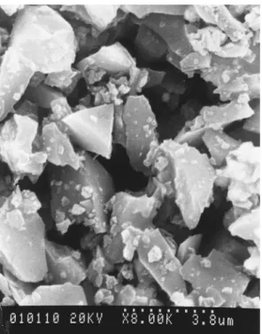
The metal matrix powder used in this experiment was electrolytic copper powder (99.7% pure). The particle morphology was dendritic and average size was 30µm. Figure 1 shows the SiCppowder (average powder size is 4µm) used as reinforcements.
To obtain optimal bonding between SiCpand Cu particles and a completely continuous copper film on SiCp, the following steps were followed.
2.1 Surface Treatment
Surface cleaning of SiCpwas accomplished by immersing it in acetone under ultrasonic vibration for 30 min. After rinsing well with deionized water, and heat-ing at 873 K for 3 hr in an air-dryheat-ing oven, the SiC was slightly ground to break agglomerated particles.
ORDER REPRINTS
486 SHU AND TU
Figure 1. SEM micrograph of SiCp.
2.2 Sensitization and Activation
The cleaned SiCpsamples were sensitized in a solution containing stanous chloride (SnCl2⋅2H2O) and hydrochloric acid (HCl) for 1 hr and then activated in a solution containing palladium chloride (PdCl2) and hydrochloric acid for a few hours.
2.3 Electroless Copper Process
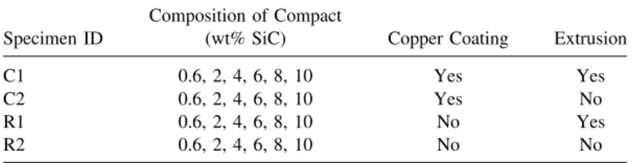
Before the procedure of mixing, continuous stirring, and rinsing, the cleaned SiCp was put into CuSO4 ⋅ 5H2O (20 g/l) and KNaC4H4O6(50 g/l) individually, shaken by ultrasound, and then HCOH (36%) and NaOH were added. The pH value of the solution was adjusted by adding NaOH until the pH value approached 13, then the copper film was created. The thick film was obtained by later immers-ing it in Fehlimmers-ing solution. The components of Fehlimmers-ing solution are as follows: CuSO4⋅ 5H2O (10 g/l); KNaC4H4O6(25 g/l); HCOH (50 ml/l); and NaOH (7 g/l). The mixture of the constituent powders with the preselected SiC percentages (0.6, 2, 4, 6, 8, and 10 wt%) was milled with aluminum balls as the grinding medium in Ar atmosphere, and cold formed by pressing the powders with a unit pressure of 450 MPa.
Table 1. Specimen Classification Composition of Compact
Specimen ID (wt% SiC) Copper Coating Extrusion
C1 0.6, 2, 4, 6, 8, 10 Yes Yes
C2 0.6, 2, 4, 6, 8, 10 Yes No
R1 0.6, 2, 4, 6, 8, 10 No Yes
R2 0.6, 2, 4, 6, 8, 10 No No
A series of compacts was heated to 1073 K for 4 hr in hydrogen, and then extruded at 973 K by an indirect extrusion method with a 15:1 extrusion ratio. The specimen classifications are summarized in Table 1.
Composite testing involved measurements of the density, hardness, ultimate stress, volume electrical resistivity, and CTE. The density of the Cu–SiCp compos-ites was measured by using the buoyancy (Archimedes) method. The hardness measurement was performed with a Rockwell hardness tester. Uniaxial tensile testing with a constant cross-head speed of 1.0 mm/min was carried out on a Instron testing machine at room temperature; specimens were machined according to ASTM E8 standard. The four-probe method was used for measuring the electri-cal resistivity.
The CTE value was obtained using a thermal mechanical analyzer. The prod-ucts were characterized by means of X-ray diffraction as well as OM, SEM, and transmission electron microscopy (TEM). The particle diameter was measured using a Honeywell UPA particle size analyzer. EDM testing was performed on a Charmer CM30A EDM machine.
3.0 RESULTS AND DISCUSSION
3.1 Change of Powder Particles by Electroless Plating and Milling
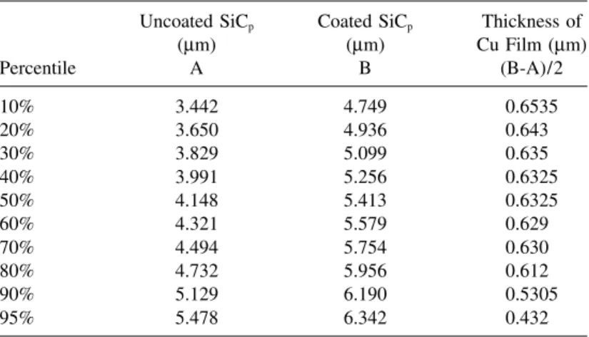
Electroless Cu-coated SiCpsamples are shown in Figure 2. The coated cop-per film is homogenous and continuous. The thickness of the Cu film given in Table 2 was found to be about 0.6µm.
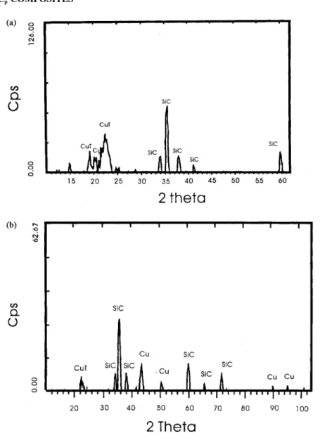
Figure 3 shows the X-ray diffraction (XRD) patterns of the treated and the copper-coated SiCp particles. Figure 3a shows the XRD pattern of SiCp (which was obtained before adding HCOH and NaOH); the copper tartrate (CuT) and SiC peaks were detected, and no detectable peak appeared for palladium. This is because the concentration of palladium was extremely low and palladium spreads over the surface at the atomic level. After coating, as shown in Fig. 3b, three new peaks appeared at 2θ ⫽ 43.2, 50.6, and 74.5°. These results indicate that the Cu was coated on the SiC particle.
Figure 4 shows the change in powder–particle morphology of 2 wt% SiC– Cu powder following 8 hr of ball milling. The powder particles underwent
ORDER REPRINTS
488 SHU AND TU
Figure 2. SEM micrograph of SiCpcoated with Cu.
Table 2. Particle Size of SiCpDetermined Using Honeywell UPA Uncoated SiCp Coated SiCp Thickness of
(µm) (µm) Cu Film (µm) Percentile A B (B-A)/2 10% 3.442 4.749 0.6535 20% 3.650 4.936 0.643 30% 3.829 5.099 0.635 40% 3.991 5.256 0.6325 50% 4.148 5.413 0.6325 60% 4.321 5.579 0.629 70% 4.494 5.754 0.630 80% 4.732 5.956 0.612 90% 5.129 6.190 0.5305 95% 5.478 6.342 0.432
Figure 3. The XRD patterns of the particles. (a) SiCpactivated with palladium; (b) SiCpplated with copper.
peated flattening and fracturing as a result of the collisions of the milling balls in the mechanical milling mixture, and consequently became fine powder of flattened particles which look different from the original dendritic shape.
3.2 Density
The true densities obtained by Archimedes’ law and the theoretical values are listed in Table 3 for comparison. It was observed that the density of the
ORDER REPRINTS
490 SHU AND TU
Figure 4. The change in powder–particle morphology of 2 wt% SiCp–Cu for plated samples after 8 hr of ball milling.
posite with electroless copper-plated SiCpfor all wt% SiCpis a little higher than that without the coating.
The porosity can be determined by the following equation (25):
fp⫽ 1 ⫺ ρ/ρ0 (1)
where fpis the pore volume fraction,ρ is the measured density, ρ0is the theoretical density.
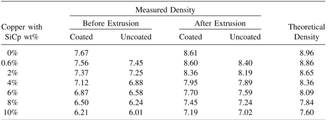
Table 3. Sample Density
Measured Density
Before Extrusion After Extrusion
Copper with Theoretical
SiCp wt% Coated Uncoated Coated Uncoated Density
0% 7.67 8.61 8.96 0.6% 7.56 7.45 8.60 8.40 8.86 2% 7.37 7.25 8.36 8.19 8.65 4% 7.12 6.88 7.95 7.89 8.36 6% 6.87 6.58 7.70 7.59 8.09 8% 6.50 6.24 7.45 7.24 7.84 10% 6.21 6.01 7.19 7.02 7.60
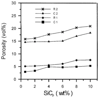
Figure 5. Variation of porosity with SiCpcontents for the Cu–SiCpcomposite.
Figure 5 reveals that, compared to the composites made by the extrusion process, all of the composites made by the as-sintering process had relatively high porosity. For the composites made by extrusion, although the porosity increased with increasing SiCpcontent, the porosity remained comparatively low.
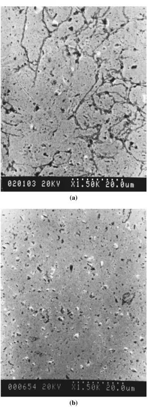
Figure 6 shows SEM micrographs of polished samples of composites con-taining 2 wt% SiCp. The composite made by the as-sintering method (Fig. 6a) contained a large amount of pores, with most of the pores ranging in size from 2 to 40 µm. Some large pores were observed to have flat shapes. However, no large pore was observed in the composite made by the extrusion method (Fig. 6b). In Figure 5, it also can be observed that the porosities of C1 and C2 specimens are slightly lower than those of R1 and R2 specimens individually; this indicated that the density of composites can be improved to a certain extent by coating a copper film on SiCp. This is presumably caused by better sintering ability between coated SiC–Cu compared to SiC–Cu particles. A hot extrusion process can im-prove the density of the composites up to 95% of the theoretical density value. As shown in Figure 5, the porosity of the coated 2 wt% SiCp composite significantly decreased following the extrusion process.
3.3 Tensile Strength
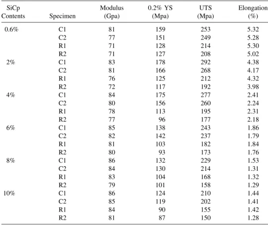
The tensile properties of various Cu–SiCpspecimens are given in Table 4. It shows that apparently the tensile properties have been significantly improved through hot extrusion. This is probably because of reduction in the amount and size of the porosity after hot extrusion, interfacial bonding enhancement between
ORDER REPRINTS
492 SHU AND TU
(a)
(b)
Figure 6. SEM micrographs of the 2 wt% SiCp–Cu composites (a) as sintering, and (b) extruded.
Table 4. Tensile Test Results
SiCp Modulus 0.2% YS UTS Elongation
Contents Specimen (Gpa) (Mpa) (Mpa) (%)
0.6% C1 81 159 253 5.32 C2 77 151 249 5.28 R1 71 128 214 5.30 R2 71 127 208 5.02 2% C1 83 178 292 4.38 C2 81 166 268 4.17 R1 76 125 212 4.32 R2 72 117 192 3.98 4% C1 84 175 277 2.41 C2 80 156 260 2.24 R1 78 113 195 2.31 R2 77 96 177 2.18 6% C1 85 138 243 1.86 C2 82 142 237 1.79 R1 81 103 182 1.84 R2 80 93 173 1.76 8% C1 86 132 229 1.53 C2 84 130 214 1.31 R1 83 104 168 1.32 R2 79 101 158 1.29 10% C1 86 124 210 1.44 C2 85 119 202 1.41 R1 84 90 155 1.42 R2 81 87 150 1.28
SiC and the matrix, grain reinforcement of Cu matrix, and a more homogeneous distribution of SiC after hot extrusion. The wt% of SiCpand the electroless plating process were found to tremendously influence the tensile property of copper ma-trix composite. Figure 7 demonstrates that ultimate stress decreases with an in-creasing amount of uncoated SiCp. There is a maximum value of ultimate stress at 2 wt% if the SiCpparticles are electroless plated with copper. This phenomenon is caused by particle reinforcement. The strength of composite decreases if the SiCpis increased, because more defects are produced. The tensile strength of com-posites with uncoated SiCp is lower than the composites with electroless-plated SiCp. The strength of the composite is reduced by the presence of SiCpowing to the poor bonding between the uncoated SiCpand copper.
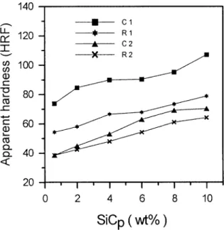
3.4 Hardness
Figure 8 shows the change in the Rockwell hardness number of Cu–SiCp composites for various SiCpwt% made by various methods. The hardness value increases with increasing SiCpwt%. Generally, the hardness of material increases
ORDER REPRINTS
494 SHU AND TU
Figure 7. The ultimate stress in Cu–SiCpcomposites.
with increase of material strength. However, in the present work, the strength decreased with increasing SiCp wt% (Fig. 7). As can be seen in Figure 5, the porosity increases with increasing SiCp wt%; this is responsible for the corsponding decreasing stress and increasing hardness tendencies (Figs. 7 and 8, re-spectively). The former tendency has been explained in section 3.3. The latter
Figure 8. The Rockwell hardness number of Cu–SiCpcomposite.
increasing hardness tendency is qualitatively explained as follows: the Cu–SiCp hardness is probably determined by the composite effect of porosity and SiC parti-cles. It is apparent that the Cu–SiC interface increases with increasing SiCpwt%, thus hindering more seriously the Cu slipping and resulting in increased hardness. In this work, the pore sizes were only about one-half to one-third of SiCpsizes (Fig. 6) and the porosity increased only mildly with SiCp(Fig. 5). Therefore, the effect of porosity on hardness would appear much less important than the domi-nant effect of Cu/SiC interface (i.e., the inherent high SiC hardness).
The promoted bonding between SiCpand Cu by copper-coating method re-strains more effectively elastic and plastic deformation of the composites, leading to higher hardness. Much lower porosity can be achieved through the extrusion process, rendering higher composite hardness.
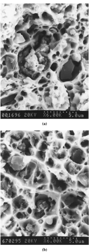
3.5 Fracture Surface
SEM micrographs of the fracture surfaces of the composites with 0.6 wt% uncoated SiCpcontent having poor interface bonding between the matrix and the particle is shown in Figure 9a. SiCpshows relatively flat surfaces, and a sample with 2 wt% coated SiCpcontent (where the copper film can be seen on the surface of SiCp) is shown in Figure 9b. In both samples, fracture appears to initiate at the SiCp particles, with the fracture surfaces characterized by the presence of large microvoids with SiCpparticles at the center of each dimple. The crack may propa-gate along the interface between SiCpparticles and matrix, and within SiCp parti-cles. In addition to the normal ductile dimple fracture of the matrix, there are two types of fracture behavior involved with SiCpparticulate: fracture of SiCpand Cu– SiCpinterface decohesion. In Figure 9a, the fracture surface shows the presence of decohesion at the Cu–SiCp interface. However, the occurrence of SiCp fracture was observed in Figure 9b, and this indicates that there was load transfer from the matrix to the SiCpparticulate.
3.6 Electrical Resistivity
The electrical resistivity of composites depends on the size and number of microweldments developed between particles during sintering. Figure 10 indicates that the electrical resistivity is increased with a higher SiCpcontent.
The effective electrical resistivityσeffof two-phase composite materials can be determined by the simple rule of mixture (ROM) when the electrical resistivity of both phases are comparable, i.e.,σ1⬃ σ2(26), and
σeff ⫽ f1⫻ σ1⫹ f2σ2 (2) where fiis the volume fraction andσiis the electrical resistivity of phase i.
ORDER REPRINTS
496 SHU AND TU
(a)
(b)
Figure 9. SEM micrographs of the fracture surface of composites in (a) 0.6% uncoated SiCp, and (b) 2 wt% coated SiCp.
Figure 10. Measured and predicted electrical resistivity of Cu–SiCpcomposites.
Theσeff value is 166,001µΩ-cm if the ROM model is used to calculate the effective electrical resistivity of composite with 0.6 wt% of SiCpcontent, and a large discrepancy from experiment data was found.
When the difference between electrical resistivity of constituent phases is increased, the dependence of the effective resistivity on the volume fraction be-comes nonlinear, and the electrical resistivity can be represented by the effective medium theory (EMT). EMT considers a spherical entity consisting of a single phase embedded in the surrounding effective medium, with the following relation given in reference 27: f1⫻ σ 1⫺ σeff σ1⫹ 2σeff ⫹ f2⫻ σ 2⫺ σeff σ2⫹ 2σeff ⫽ 0 (3)
where the surface electrical resistivity of copper and SiCp are 1.130 and 1.0 ⫻ 107µΩ cm, respectively. The electrical resistivity of the copper composite calcu-lated by the above model gives close results to the experimental data shown in Figure 10.
3.7 CTE
Because the CTEs for Cu and SiCpare 16.9 ⫻ 10⫺6K⫺1 (293–573 K) and 5.0⫻ 10⫺6K⫺1, respectively (28,29), it is expected that the CTE of the composite would be lowered with the addition of SiCp. The CTE of a particle-reinforced composite is often estimated by three popular models (30), for which the ROM model is often considered inappropriate because it does not take into account
ORDER REPRINTS
498 SHU AND TU
the microstructure and strain interactions. The Turner’s model (31), considering uniform hydrostatic stresses exit in the phases, predicts the CTE of a composite by
αc ⫽ α
pfpkp⫹ αmfmkm
fpkp⫹ fmkm
(4) where αc, αp, and αm are the CTEs of composites, reinforcements, and matrix, respectively; km is the bulk modulus of matrix; and the Kerner’s model (32) ac-counts for both the shear and isostatic stress developed in the component phases and determines the composite CTE by
αc ⫽ αpfp⫹ αmfm⫹ (αp⫺ αm) fpfm kp⫺ kp kpfp⫹ kmfm⫹ 3kpkm 4Gm (5)
where Gm is the shear modulus of matrix.
The measured and calculated results of linear thermal expansion curves for Cu–SiCpcomposite are presented in Figure 11. The results show that the CTE decreases as the SiCpweight fraction increases. The experimental CTEs are much higher than these predictions. The results reflect the weak bonding between SiCp and Cu, which provides little constraint on the expansion or contraction of the copper matrix.
Figure 11. Measured and predicted linear thermal expansion of the Cu–SiCpcomposites (200– 500°C).
3.8 Material Removal Rates on EDM
Metal removal rate is an important parameter for evaluating the machining performance of EDM for a particular working setup, and the machining rate de-pends on the electrode manufacturing variable. Material removal rate can be ex-pressed as follows (33):
Wm ⫽ Km⋅ τaon ⋅ Ibp⋅ 106 τon⫹ τoff
(6) where Wm is the material removal rate (mm3/min); Km, a, and b are coefficients to be determined by test condition; and τon and τoff (in µsec) are pulse on time and pulse off time, respectively.
A higher discharge current leads to higher discharge energy and energy den-sity. Thus, more material can be melted which increases the removal rate. Figure 12 shows that the material removal rate increases with an increase in applied current. In general, the removal rate varies very little under the normal condition of pulse off time. The pulse on time is taken to be 150µsec in this research, so the material removal rate increases with the increase of applied current. The maximum removal rate was found for Cu–2wt% SiCpcomposite. This suggests that EDM with 2 wt% SiCp of copper electrode is the better choice for cutting mold steel when pulse time is 150µsec.
Figure 12. Relationship of the material removal rate, applied current, and SiCpwt%. (τon⫽ 150 µsec; τoff⫽ 150 µsec; positive electrode; SKD61 workpiece.)
ORDER REPRINTS
500 SHU AND TU
Table 5. The Product ofλ and Tm Fusion Temperature Thermal Conductivity
Material Tm(K) λ(w/mk) ⫻ 104 λ ⫻ Tm(w/m)
Cu 1357 369 40.0
SiCp 2473 67 14.7
3.9 Electrode Wear Ratio
An ideal EDM tool electrode is the one that not only can remove a large amount of material from the workpiece, but also is capable of resisting self-ero-sion.
Table 5 shows the fusion temperature and thermal conductivity (λ) for Cu and SiCp. The electrode wear is roughly proportional to the product of thermal conductivity (λ) and fusion temperature (Tm) (34). Although the fusion tempera-ture of SiCp is high, because its thermal conductivity is very small, the product of thermal conductivity and fusion temperature (λ ⫻ Tm) for SiCpis less than that for Cu, so the (λ ⫻ Tm) values for the composite are decreased by increasing SiCp wt%.
The electrode wear P is affected by the discharge pulse energy, which is determined by discharge current and pulse on time, as shown in the following formula (32):
Figure 13. Relationship of the tool wear ratio, applied current, and SiCpwt% (τon ⫽ 150 µsec; τoff⫽ 150 µsec; positive electrode; SKD61 workpiece.)
P ⫽
冮
τon
0
u(t)dt (7)
where u(t) is the discharge voltage in V; i(t) is the discharge current in A; and τon is the pulse on time in µsec. This formula indicates that the increase of dis-charge current and pulse on time increases the disdis-charge pulse energy as well as the electrode wear.
The variations of tool wear ratio of the electrode with various SiCp wt% operating at different currents are shown in Figure 13. In general, the tool wear ratio is proportional to the applied current. As discussed above, the higher dis-charge current leads to higher energy, thus both the material removal rate and tool wear ratio are increased. It also can be observed that the tool wear ratios are almost the same when SiCpcontents are under 4 wt%, and they increase dramati-cally when SiCpcontents are larger than this value. Theλ ⫻ Tmvalue of composite was decreased by increasing SiCp contents, leading to increased wear ratio with increasing SiCpcontents.
4.0 CONCLUSIONS
The mechanical properties of Cu/SiCp metal–matrix composite, made by powder sintering and extrusion, can evidently be improved from the pure copper counterpart. This is due to the strengthening effect of SiC powder dispersed into the Cu matrix. It was found that an improved bonding could be achieved by activa-tion of SiC powder surface through electroless coating of Cu onto SiC powder. From the results of the present work, it was found that a continuous copper film coated on SiCpby electroless copper coating to form a uniform distribution of SiCpin Cu matrix is possible. A lower electrode wear ratio can be achieved for EDM testing, and the 2 wt% SiCpof copper electrode is the better choice for cutting mold steel when pulse time is 150µsec.
5.0 ACKNOWLEDGMENTS
The authors thank the National Science Council of the Republic of China for the financial support under Grant NSC86-2216-E-009-016 for the experimental aspect of the study. Special thanks are acknowledged to one of the reviewers, who reviewed carefully and made many valuable suggestions on the paper.
6.0 REFERENCES
1. Her, M.G.; Weng, F.T. Int. J. Adv. Manuf. Technol. 2001, 17, 715.
2. Marafona, J.; Wykes, C. Int. J. Mach. Tools Manuf. 2000, 40, 153.
3. Chen, Y.; Mahdavian, S.M. Wear 1999, 236, 350.
ORDER REPRINTS
502 SHU AND TU
4. Park J.; Keller, S.; Carman, G.P.; Hahn, H.T. Sens. Actu. A: Phys. 2001, 90, 191.
5. Samuel, M.P.; Philip, P.K. Int. J. Mach. Tools Manuf. 1997, 37 (11), 1625.
6. German, R.M.; Hens, K.F.; Johnson, J.L. Int. J. Powder Metall. 1994, 30 (2), 205.
7. Kenny, F.E.; Balbahadur, A.C.; Lashmore, D.S. Wear 1997, 203, 715.
8. Hart, R.R.; Wonsiewicz, B.C.; Chin, B.Y. Metall. Trans. 1970, 1, 3163.
9. Warrier, K.G.K.; Rohatgi, P.K. Powder Metall. 1986, 29, 65.
10. Chang, S.Y.; Lin, S.J. Scripta Mater. 1996, 35, 225.
11. Zhang, J.; Laird, C. Acta Mater. 1999, 47, 3811.
12. Mortensen, A.; Pedersen, O.B.; Lilholt, H. Scripta Mater. 1998, 38, 1109.
13. Jahazi, M.; Jalilian, F. Composites Sci. Technol. 1999, 59, 1969.
14. Chang, Y.S.; Lin, S.J. Scripta Mater. 1996, 35 (2), 225.
15. Zwisky, K.M.; Grant, N.J. Metal Prog. 1961, August, 209.
16. Denisenko, E.T.; Polushko, A.; Filatova, N.A. Porosh Kovaya Metall. 1971, 10, 49.
17. Surappa, M.K.; Rohatgi, P.K. Metal. Technol. 1978, 5 (10), 358.
18. Grimes, J.H.; Scott, K.T.B. Powder Metall. 1968 11 (22), 213.
19. Rogers J. A.; Miles, D.E.; Hopkins, B.E. Powder Metal. 1973, 16, 66.
20. Kobayashi, K.F.; Tachibana, N.; Shingu, P.H. J. Mater. Sci. 1990, 25, 3149.
21. Hanada, K.; Murakoshi, Y.; Negishi, H.; Sano, T. Proceedings of the 45th Japanese
Joint Conference for the Technology of Plasticity, 1994; 760.
22. Groza, J.R.; Gibeling, J.C. Mater. Sci. Eng. 1993, A171, 115.
23. Warren, R.; Anderson, C.H. Composites 1984, 15, 101.
24. Qin, C.D.; Derby, B. Br. Ceram. Trans. J. 1991, 90, 124.
25. Yih, P.; Chung, D.D.L. J. Mater. Sci. 1999, 34, 359.
26. Kovacik, J.; Scripta Mater. 1998, 39 (2), 153.
27. Landauer, R. AIP Conference Proceedings 40, New York, 1978; 2.
28. Beer, F.P.; Johnston, E.R. Mechanical Behavior of Materials, 2nd Ed.;
McGraw-Hill: New York, 1996; 806.
29. Courtney, T.H. Mechanical Behavior of Materials, 2nd Ed.; McGraw-Hill: New
York, 1996; 46.
30. ASM Handbook, Vol. 2; American Society for Metals: Metals Park, OH, 1991; 401.
31. Sun, Q.; Inal, O.T. Mater. Sci. Eng. 1996, B41, 261.
32. Turner, P.S.; J. Res. Nat. Bur. Stand. 1946, 37, 239.
33. Zhang, J.H.; Lee, T.C.; Lau, W.S. J. Mater. Proc. Technol. 1997, 63, 908.
34. Kerner, E.H. Proc. Phys. Soc. 1956, B69, 808.