國立交通大學
材料科學與工程學系
碩 士 論 文
自組裝膠體晶體及其金屬反蛋白石結構之製備及特性分析
Fabrication and Characterization of Planar and Cylindrical
Colloidal Crystals and their Nickel Inverse Opals
研究生: 賴俊翰 (C. H. Lai)
自組裝膠體晶體及其金屬反蛋白石結構之製備及特性分析
Fabrication and Characterization of Planar and Cylindrical
Colloidal Crystals and their Nickel Inverse Opals
研究生:賴俊翰 Student: Chun-Han Lai
指導教授:吳樸偉 博士 Advisor: Pu-Wei Wu
國 立 交 通 大 學
材料科學與工程學系
碩 士 論 文
A Thesis
Submitted to Department of Materials Science and Engineering College of Engineering
National Chiao Tung University in partial Fulfillment of the Requirements
for the Degree of Master
in
Materials Science and Engineering June 2009
Hsinchu, Taiwan, Republic of China
自組裝膠體晶體及其金屬反蛋白石結構之製備及特性分析
研究生:賴俊翰 指導教授:吳樸偉 博士
國立交通大學材料科學與工程學系
摘 要
本研究以電泳披覆法 (Electrophoretic deposition) 分別製作平板及柱狀
自組裝膠體晶體於 ITO 導電玻璃及碳纖維上。以最佳化之參數所製備之平
板膠體晶體具有單一光子能隙 (Photonic band gap) ,其能隙位置會隨著實
驗中使用之微球尺寸而改變;而柱狀膠體晶體由於反射面積有限,加上自
組裝之微球延柱狀表面呈輻射狀之排列,導致其光子能隙強度減弱,然而,
其反射峰之半高寬卻因柱面之特性而增加。另外,柱狀膠體晶體表面由於
入射光之散射,因此可觀察到彩虹般的平行線。 本研究接著以定電壓 1 V
在 50 ℃下進行電鍍 (Electrodeposition) ,將鎳填入膠體晶體之孔隙中,製
備金屬反蛋白石結構,再以 250℃之熱處理去除結構內之聚苯乙烯微球。由
於膠體晶體之侷限,金屬反蛋白石結構具有特定的成長方向。另外,隨著
熱處理的時間增加,聚苯乙烯可完全被移除,同時結晶性也隨之增強,電
阻率隨之下降。在光學分析上,平板鎳之反蛋白石結構具有光子能隙邊界
Fabrication and Characterization of Planar and Cylindrical
Colloidal Crystals and their Nickel Inverse Opals
Student: Chun-Han Lai Advisor: Dr. Pu-Wei Wu
Department of Materials Science and Engineering
National Chiao Tung University
Abstract
Planar and cylindrical colloidal crystals were fabricated by electrophoretic deposition with 460 and 660 nm PS microspheres on ITO-glass and carbon fibers, respectively. To improve the quality of the colloidal crystals, variables including microsphere concentration, electrical field, and deposition time were investigated. With the optimized process, the multi-layer colloidal crystals with ordered structure could be obtained within 1 hr. In planar colloidal crystals, we observed an obvious photonic band gap in reflectance spectra. In contrast, a series of iridescent fringes was present in cylindrical colloidal crystals. To fabricate Ni inverse opals, potentiostatic electrodeposition was carried out on the colloidal crystals. With careful control in the plating step, we were able to obtain inverse opals in finite thickness. To remove the PS microspheres, the deposited samples underwent chemical dissolution using ethyl acetate and thermal oxidation at 250 ℃ after the electrodeposition. The heat treatment was able to clean the PS microspheres without structure distortion. Meanwhile, the crystallinity of the Ni inverse opals was improved during the heat treatment.
Acknowledgements
兩年的研究所生涯,倏忽即逝。此論文的完成,不過是這兩年的一小
片段,而知識和認知的累積,卻是這兩年最大的收穫。在此要感謝這兩年
研究生活中陪我走過的每一個人;因為與你們每個人的相遇,使得這份論
文能夠以我現有的知識順利完成。
首先,要感謝的是父親、母親及家人們,你們打造了一座完美的避風
港,在心理上及經濟上給予我相當的支持,使我能在他鄉一心一意的做研
究。接著感謝女友,有妳的相伴,碩二生活充滿光彩,感謝妳總能在失意
時給予我最大的關懷,並以歡笑帶給了我對生活的期待。
接著,要感謝實驗室的大家。首先是苡叡學長,感謝你在實驗上及專
業知識上給予我最大的幫助,讓我在嘗試的過程中找到最近的路;感謝勝
結大哥,在我還是專題生的時候在凌晨三點協助拍攝 SEM;感謝雲閔學長,
總是提供我生活上的小智慧,並陪我一起跨越美國國界。感謝于凡學妹、
冠廷學弟在我碩一參與的計畫中大力相助,使計畫得以順利結案。感謝同
屆的戰友:境妤、和成、張三角、梁阿夢還有柚子,在最後幾個月於實驗
上交換心得,於論文上給予協助。
本論文中,特別感謝楊玉麟學長於光學量測上之協助與討論,陳智教
授實驗室於儀器協助及操作之指導,岱民同學於電性量測上之協助與討論,
Contents
摘要...i Abstract...ii Acknowledgements...iii Contents...iv List of Figures...vii List of Tables...xiv Chapter 1 Introduction...1Chapter 2 Literature Review...3
2.1 Photonic Crystals...3
2.2 Electrophoretic Deposition...7
2.3 Electrodeposition...10
Chapter 3 Experimental...11
3.1 Materials.. ...13
3.1.1 Synthesis of Polystyrene Microspheres...13
3.1.2 Preparation of Suspensions...13
3.2 EPD for Colloidal Crystals...14
3.2.1 Pretreatment of Planar Substrates...14
3.2.2 Fabrication of Planar Colloidal Crystals...14
3.2.3 Preparation of Circular Electrodes...14
3.2.4 Fabrication of Cylindrical Colloidal Crystals...15
3.3 NED for Inverse Opals...16
3.4 Removal of Polystyrene Template...17 3.4.1 Chemical Dissolution...17 3.4.2 Thermal Oxidation...17 3.5 Instrument...18 3.5.1 Morphological Observation...18 3.5.2 Characterization...18
Chapter 4 Results and Discussion on EPD Process...20
4.1 Suspension and Substrates...21
4.1.1 Microsphere Concentration in Suspension...22
4.1.2 Shape of Substrates...24
4.2 Fabrication of Planar Colloidal Crystals (PCCs)...25
4.2.1 Electric Field in EPD Process...25
4.2.2 Deposition Rate for Planar EPD...28
4.3 Fabrication of Cylindrical Colloidal Crystals (CCCs) ...31
4.3.1 Applied Voltage in EPD Process...31
4.3.2 Deposition Rate for Cylindrical EPD...34
Chapter 5 Results and Discussion on NED and PS Removal Process...41
5.1 Fabrication of Planar Nickel Inverse Opals...44
5.1.1 Current Density in NED process...44
5.1.2 Deposition Rate for Planar NED...47
5.2 Fabrication of Cylindrical Nickel Inverse Opals...52
Chapter 6 Measurements and Analyses...64
6.1 Electrical Measurements...64
6.1.1 Sheet Resistance of Planar Inverse Opals...64
6.1.2 Resistivity of Cylindrical Inverse Opals...65
6.2 Optical Analyses...68
6.2.1 Reflection Spectra of Colloidal Crystals...68
6.2.2 Light-Diffracting Fringes of Cylindrical Colloidal Crystals...71
6.2.3 Reflection Spectra of Nickel Inverse Opals...73
Chapter 7 Conclusions...77
List of Figures
Figure 2.1 First hybrid band structure of photonic crystal in a face-centered arrangement. ... 4 Figure 2.2 Method to construct a FCC structure with non-spherical shapes and the forbidden
band diagram of the structure. ...4
Figure 2.3 A schematic illustration of the principle of the dielectric mirror for 1-D PCs. ...5 Figure 2.4 (a) SEM image of a PBG optical fiber and (b) the optical micrograph of the field
intensity pattern at the optical exit face. ...5
Figure 2.5 Photonic band diagram of a silicon diamond opal. ...………6 Figure 2.6 A plot of Free energy (△G) dependence on distance (H) from a particle surface (a)
before and (b) after extending the repulsive field. ...………7
Figure 2.7 A volume fraction-electric field phase diagram for the EPD. ...………8 Figure 2.8 SEM image of cylindrical colloidal crystals fabricated by capillary force within a
micro-capillary. ...9
Figure 2.9 SEM image of top view of cylindrical colloidal crystal within a mold. ...9 Figure 2.10 Time dependence of current in fabrication of inverse opals by electrodeposition.
The numbered arrows indicate the valleys of current. Inset shows the times when the valleys appeared (●) and the intervals between each valley (△). ...10
Figure 3.1 Schematic diagrams for fabrication of (a) planar and (b) cylindrical inverse
opals. ...11
Figure 4.2 Electrophoretic mobility of suspension (a) PS-460 and (b) PS-660. ...22 Figure 4.3 SEM images of EPD layers prepared in PS-460 with various microsphere
concentrations of (a) 10 g/L and (b) 2.5 g/L. The electrical field was fixed at 10 V/cm for 3 min. The scale bars are 3 μm. ...23
Figure 4.4 SEM images of EPD layer made in PS-660 with microsphere concentrations of (a)
25 g/L and (b) 10 g/L. The electrical field was fixed at 10 V/cm for 10 min. The scale bars are 5 μm. ...23
Figure 4.5 SEM images of EPD layer on (a) ITO glass and (b) carbon fiber. The insets
provide the SEM images of each substrate. The scale bars are 5 μm in the figure and 2 μm in the inset. ...24
Figure 4.6 Thickness versus electric field for the colloidal crystals made of PS-660. The
EPD fabrication time was 15 min. ...25
Figure 4.7 SEM images of PCC-660s fabricated in PS-660 under (a) 5 V/cm, (b) 10 V/cm,
and (c) 20 V/cm for 15 min. The scale bars are 2 μm. ...26
Figure 4.8 Thickness versus electric field for the colloidal crystals made of PS-460. The
EPD fabrication time was 10 min. ...27
Figure 4.9 SEM images of PCC-460s on ITO glass fabricated under (a) 10 V/cm, (b) 15 V/cm,
and (c) 20 V/cm for 15 min. The scale bars are 2 μm. ...27
Figure 4.10 Evolution of current density vs. time during the EPD process under (a) 10 V/cm
using PS-660 microspheres and (b) 15 V/cm using PS-460 microspheres. ...28
Figure 4.11 Thickness versus EPD time for the PCC-660 (■) and PCC-460 (☆). The applied electric field was 10 V/cm in PS-660 and 15 V/cm in PS-460. ...28
Figure 4.12 SEM images of PCC-660s fabricated under 10 V/cm for (a) 3, (b) 6, (c) 9, (d) 12,
and (e) 15 min, respectively. All scale bars are 5 μm. ...29
Figure 4.14 The SEM images of CCC-460s made of (a) 5 V, and (b) 10 V. The fabrication
time was 30 sec. The scale bars are 5 μm in (a) and 10 μm in (b). ... 32
Figure 4.15 Diameter versus voltage for the CCC-460s (☆) and CCC-660s (■). Their
fabrication time was 30 sec. ...32
Figure 4.16 SEM images on the surface morphology of CCC-660 made of (a) 10 V and (b) 20
V, as well as CCC-460 made of (c) 10V and (d) 20V. The fabrication time was 30 sec, and the scale bars are 5 μm. ...33
Figure 4.17 Time dependence of current density for (a) CCC-660 and (b) CCC-460 during
cylindrical EPD process. The applied voltage was fixed at 10 V. ...34
Figure 4.18 Diameter versus EPD time for the CCC-660 (■) and CCC-460 (☆) fabricated in suspensions under a voltage of 10 V. ...35
Figure 4.19 SEM images for the surface morphology of CCC-660s made of 10 V in PS-660
for (a) 2 min, (b) 4 min, and (c) 8 min, respectively. All scale bars are 5 μm. ...36
Figure 4.20 SEM images of the surface morphology of CCC-460s made of 10 V in PS-460
for (a) 2 min, (b) 4 min, and (c) 8 min. All scale bars are 5 μm. ...37
Figure 4.21 Diameter versus EPD time for the CCC-660 (■) and CCC-460 (☆) fabricated in suspensions under a voltage of 10 V. ...38
Figure 4.22 Optical microscopy images of CCC-460 self-assembled in PS-460 for (a) 10 min
and (b) 50 min. The scale bars are 200 μm. ...39
Figure 4.23 Optical microscopy images of CCC-660 self-assembled in PS-660 for (a) 10 min,
Figure 5.3 SEM images on the surface morphology of (a) CCC-460 and (b) CCC-660. The
scale bars are 5 μm. Insets display optical microscopic images for CCCs with scale bars of 100 μm. ...……….43
Figure 5.4 Time dependence of current density during the Ni electrodeposition at pH of 5.2
and 1 V on PCC-460 (red) and PCC-660 (black). The inset plot shows the transition points that were determined by the variation of current density at initial stage. Inset axes are identical with the principal plot. ...………44
Figure 5.5 XRD patterns for planar (a) NIO-660 and (b) NIO-460. ...……….45 Figure 5.6 SEM images of multi-domains in planar (a) NIO-660 (b) NIO-460. The insets
exhibit the cross-section view of each sample. All scale bars are 5 μm. ...46
Figure 5.7 SEM images of different lattice arrangement in planar NIO-460;(a) Rhombohedral,
(b) FCC-(110), (c) FCC-(111), and (d) FCC-(100). All scale bars are 2 μm. ... ………47
Figure 5.8 Photographic images of multi-layer (a) NIO-660 and (b) NIO-460. The scale
bars are 500 μm. The insets in each figure display the color of the semi-layer samples changes that changes with the view angle. ...………….48
Figure 5.9 Layer number versus NED time for the planar NIO-660s (■) and NIO- 460s (☆) . The applied voltage was 1 V... ………...49
Figure 5.10 SEM images of NIO-660s with different filling fractions. Inset sketch shows a
schematic diagram of different filling fractions. The scale bars are 2 μm. ...49
Figure 5.11 SEM images of NIO-660 prepared under 1 V for (a) 10, (b) 15, (c) 20, (d) 25, and
(e) 30 min, respectively. All scale bars are 2 μm. ...50
Figure 5.12 SEM images of the NIO-460 prepared under 1 V for (a) 5, (b) 8, (c) 10, (d) 20,
and (e) 30 min, respectively. All scale bars are 2 μm. ...51
stages of deposits inside the PS template at each point indicated by arrows, and the plot shows the transition points that were determined by variation of current density at initial stage. Inset axes are i dentical with the principal plot. ...….52
Figure 5.14 SEM images for the (a) semi-layer and (b) multi-layer CIO-660s. Insets
provide the magnified images. The scale bars in the insets are 2 μm. ...53
Figure 5.15 EDX analysis of the as-prepared CIOs. ...……….54 Figure 5.16 SEM images in the (a) cross-sectional and (b) side views for CIO-660, as well as
(c) cross-sectional and (d) side views for CIO-460. The fabrication time was fixed at 10 min. The scale bars are 5 μm. ...………...55
Figure 5.17 Optical microscopic images of the CIO-660s after NED process for (a) 30 sec, (b)
1 min, and (c) 10 min. Figure (d) is the magnified image of (b). The inset in (a) provides the image of a pure carbon fiber. The scale bars are 20 μm in (a) to (c), and 10 μm in (d). ...……….56
Figure 5.18 Thickness versus NED time for the CIO-660 (■) and CIO- 460 (☆) fabricated with an applied voltage of 1 V. ...………57
Figure 5.19 SEM images for the CIOs made of NED for different deposition time; (a)
CIO-660 for 10 min, (b) CIO-660 for 30 min, (c) CIO-460 for 10 min, and (d) CIO-460 for 30 min. All scale bars are 10 μm. ...………..58
Figure 5.20 SEM images of a bundle (3000 CFs) in (a) CIO-660s and (b) CIO-460s made of
NED for 20 min. Insets show the magnification view for the CIOs. The scale bars are 20 μm in the figures and 2 μm in the insets. ...58
50℃. The immersion time was 2 days. The scale bars are 2 μm. ..……..60
Figure 5.23 TGA profiles for the CFs, PS microspheres, and Ni coating. ..…...………61 Figure 5.24 SEM images for the NIO-460s after thermal oxidation at (a) 250, (b) 350, and (c)
450 ℃ for 2 days. Insets show the cross-sectional view for the samples. The scale bars are 1 μm in the figures and 500 nm in the insets. ...…..62
Figure 5.25 X-ray diffraction patterns for (a) the NIO-460 after heat treatment at various
temperatures, (b) Ni from JCPDS 04-0850, and (c) NiO from JCPDS 47-1049. ...63
Figure 6.1 Optical microscopic image of gold electrodes on the NIO for electrical
measurements. The sketch illustrates the setting in measurement. ..…..…64
Figure 6.2 Plot of sheet resistance with respect to the layer number for NIO-660 (■) and
NIO-460s (☆). The values for the as-deposited nickel film (○) and ITO substrate (◆) are shown on the left for comparison purpose. ...65
Figure 6.3 Optical microscopic image of silver electrodes on the CIO for electrical
measurement. The sketch illustrates the setting in measurement. ..…....….66
Figure 6.4 A plot of resistivity with respect to layer number for NIO-660s (■) and NIO-
460s (☆). ...……….….67
Figure 6.5 Simulated hybrid band structure of FCC with an index difference of 0.59. ...68 Figure 6.6 Reflectance spectra recorded from (a) PCC-460 and (b) PCC-660. ..…...69 Figure 6.7 Reflectance spectra recorded from (a) CCC-460 and (b) CCC-660 for different
EPD time. ...70
Figure 6.8 Color fringes in top view for (a) CCC-460 and (b) CCC-660. The scale bars are
200 μm. The fabrication times were 10min and 50 min, respectively. ...71
Figure 6.9 A schematic for theoretical calculation of fringe formation. ..…………...73 Figure 6.10 Wavelength of fringes versus the s/D plot of the CCCs for m = 1. The inset bars
diagram. ...73
Figure 6.11 Mid-IR reflection spectra recorded from NIO-660 and Ni film. ..……...75
Figure 6.12 Mid-IR reflection spectra recorded from NIO-460 and Ni film. ...75
List of Table
Chapter 1
Introduction
Concept of photonic crystals (PCs) was first introduced in 1987 [1,2]. The PCs provide characteristic optical responses due to their artificial lattices, which amplify the resonance of electromagnetic waves at proper wavelengths. Meanwhile, at specific wavelengths, the waves in the PCs interfere with others destructively, producing a photonic bad gap (PBG). In short, devices with a PBG can reveal a high reflectance at specific wavelengths, and this property is attractive for optical applications.
To fabricate photonic crystals, materials with distinct refractive index are arranged in a periodic pattern. To date, fabrications of desirable periodic structures have received substantial attention from research groups around the world. In general, methods for fabricating the PCs can be separated into two parts: lithography in semiconductor process and self-assembly of colloids [3-5]. Lithography technique can provide high accuracy in structural design and excellent quality for the 2-D PCs. However, the inherent high cost and long processing time are the limiting factors for commercial application. Besides, it is challenging to fabricate a 3-D complex structure using this method.
In contrast, self-assembly of colloidal crystals is relatively low cost, and the process is simpler than that of the semiconductor one. Therefore, colloidal crystals self-assembled by sub-micron microspheres such as polystyrene and silica were widely studied [6,7]. The self-assembly is typically carried out in a stable suspension, Methods include physical
were also studied [12]. For example, rod-like or tubular structures were reported and their fabrication techniques utilized driving forces such as shape-confinements and capillary forces [13-16].
3-D metallic PCs have attracted considerable attention since they exhibit a complete PBG at a specific range of wavelength [5, 17-19]. To fabricate the 3-D metallic PCs, the colloidal crystals are used as a 3-D template. By filling voids within the template with high refractive index materials, inverse opals of 3-D metallic PCs can be obtained. Deposition techniques including sol-gel [20], CVD [21], electroless deposition [22], and electrodeposition [23] are commonly used to prepare inverse opals. Among them, the electrochemical route provides a simple and inexpensive way to prepare the 3-D metallic inverse opals.
In this work, we demonstrate the fabrication of colloidal crystals by electrophoretic deposition. Sequentially, we prepare their inverse opals by nickel electrodeposition (NED). After removing the PS microspheres, both planar and cylindrical nickel inverse opals are obtained.
Chapter 2
Literature Review
2.1 Photonic Crystals
In semiconductors, the propagation of electrons is confined with periodic potential induced by well-arranged ions. With these periodic potentials, these electrons work as wave packages that interact with each other, forming an “electronic band gap”. According to the wave-particle duality, the velocity of a propagating electromagnetic (EM) wave is determined by the refractive index of the material. Therefore, as the EM waves are traveling in an artificial material with periodic refractive indices, a wave diffraction will be generated from the material. A high reflectance at a regime of frequency is obtained as a result of destructive interference by the diffracting waves. Namely, this is so-called “photonic band gap (PBG)”
This PBG character was first addressed by E. Yablonovitch in 1987 [1], and was utilized to reduce the undesirable spontaneous emissions in semiconductor lasers. In the same year, S. John [2] also published a paper about theoretical calculation of photon localization within periodic structures. After two years, the first hybrid photonic band structure in face-centered lattice was developed [24]. Their experiment results are presented in Fig. 2.1. Later, the band structure was applied to non-spherical shapes, and a complete PBG for s and p polarizations were also discussed. Their fabrication scheme and results are provided in Fig. 2.2 [25]. In addition, similar simulations were also developed for the PCs with different
refractive indices are rarely changed upon different wavelengths [28]. In contrast, the refractive indices of metal are contingent on the frequency of incident waves. The metallic PCs demonstrated a photonic band edge at a specific wavelength, above which the incident light would be totally reflected [19,29].
Figure 2.1 First hybrid band structure of photonic crystal in a face-centered arrangement [24].
Figure 2.2 Method to construct a FCC structure with non-spherical shapes and the forbidden band diagram of the structure [25].
This unique feature makes the PCs attractive for optical applications. For example, the 1-D PCs in layer structure were commonly used as dielectric mirrors [30, 31]. These layers provided designed geometry that offered a 180° phase difference between the incident and
reflective EM waves [32], as shown in Fig. 2.3. Moreover, PBG optical fibers were fabricated with period 2-D PCs [15,33], as provided in Fig. 2.4(a). The incident light propagated in the middle of the fiber, and the dispersion of wave was confined inside the structure, as presented in Fig. 2.4(b). To extend the PBG to 3-D structures, a diamond structure [34] was designed to have the complete PBG, and its hybrid band structure are presented in Fig. 2.5. So far, we can conclude that the designs for the PCs are mainly based on the periodic structure and materials with distinct index of refraction.
Figure 2.3 A schematic illustration of the principle of the dielectric mirror for 1-D PCs [32].
Figure 2.4 (a) SEM image of a PBG optical fiber and (b) the optical micrograph of the field intensity pattern at the optical exit face [33].
2.2 Electrophoretic Deposition
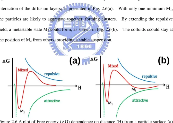
Electrophoretic deposition (EPD) is a fabrication technique involving driving of charged particles in a suspension to the working electrode [35]. Before initiaing the EPD process, a stable suspension is required. The DLVO theorem demonstrated a model to explain how the colloids could suspend stably. In a suspension system, some ions of suspension are physically attached on the colloids, forming a layer of ions that is defined as the “Stern layer”. In a negative-charged stern layer, positive ions in the solution would be attracted, raising a potential distribution from the particles to the bulk solution. The region where the potential works is defined as the diffusion layer. As the colloids are getting closer, their diffusion layers would interact with each other. Attractive and repulsive forces are generated from the interaction of the diffusion layers, as presented in Fig. 2.6(a). With only one minimum M1,
the particles are likely to aggregate together, forming clusters. By extending the repulsive field, a metastable state M2 could form, as shown in Fig. 2.6(b). The colloids ccould stay at
the position of M2 from others, providing a stable suspension.
Figure 2.6 A plot of Free energy (△G) dependence on distance (H) from a particle surface (a) before and (b) after extending the repulsive field.
electroosmosis was proposed in 1997 [36]. The model rationalized that the cluster of microspheres was formed by long range colloidal forces, including electrical field and fluid flow. Afterward, the colloidal crystals were prepared with PS microspheres in various sizes by the EPD [9]. Their optical responses as a function of particle size were discussed, and the PBG on reflectance spectra revealed a peak with high intensity about 0.8. To control the self-assembly under an electrical field, an electrophoretic phase diagram was developed [10]. The arrangement of particles can be adjusted by the particle concentration and electrical fields, as presented in Fig. 2.7. With careful control in the electrical field and suspensions, we were capable to prepare large-area colloidal crystals by electrophoretic deposition [37].
Figure 2.7 A volume fraction-electric field phase diagram for the EPD [10].
Cylindrical colloidal crystals were usually fabricated by capillary forces within a physical confinement [13-16, 38-40] or by dip-coating [41]. With a slow evaporation rate, the microspheres were self-assembled on a curved surface, as shown in Fig. 2.8. As clearly shown in Fig. 2.9, the sizes for these cylindrical colloidal crystals were limited by the mold in their fabrications. In addition, the low evaporation rate during the process was time-consuming. In contrast, the EPD process allows a tunable size. For making colloidal cylinders, the thickness can be increased with deposition time, and the length is simply
controlled by substrates. Besides, the fabrication time is shortened and not as long as that for slowly evaporation.
Figure 2.8 SEM image of cylindrical colloidal crystals fabricated by capillary force within a micro-capillary [15].
2.3 Electrodeposition
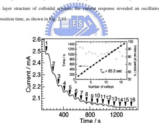
Electrodeposition is the most common method for surface modification to alter the material property. The process is carried out with two- or three-electrodes arrangement under an applied voltage. Moreover, the overpotential to drive the electroplating can be estimated via the Nearnst equation, and the amount of deposits can be calculated by Faraday’s law [42]. In electrodeposition, variables like pH value, ion concentration, temperature, and additives are usually adjusted and studied to achieve bottom-up fabrications. Likewise, to fill the void in colloidal crystals, the electrodeposition has been carried out in potentiostatic [23] or galvanostatic [43] modes. Au [44], Pt [45], Ag [44], Pd [45], Co [45], and Ni [17, 23, 46-50] inverse opals were recently fabricated through a potentiostatic electrodeposition. Because of the layer structure of colloidal crystals, the current response revealed an oscillation with deposition time, as shown in Fig. 2.10.
Figure 2.10 Time dependence of current in fabrication of inverse opals by electrodeposition. The numbered arrows indicate the valleys of current. Inset shows the times when the valleys appeared (●) and the intervals between each valley (△) [50].
Chapter 3
Experimental
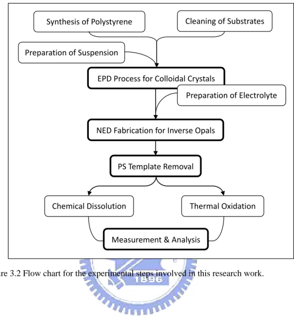
This chapter introduces a facile process to prepare high quality colloidal crystals on planar and rod-like substrates through electrophoretic depositons (EPD). In addition, nickel inverse-opals were fabricated via nickel electrodeposition (NED) in the colloidal crystals. As shown in Figure 3.1, the EPD process can fabricate ordered arrays of PS microspheres in a desirable three-dimensional pattern, while the NED can successfully convert the periodic structure into an inverse one after dissolving the PS templates. Lastly, the as-prepared samples were characterized by various instrument to determine their electrical and optical properties. Figure 3.2 provides the flow chart for the sample preparation steps involved.
Figure 3.2 Flow chart for the experimental steps involved in this research work. Cleaning of Substrates Synthesis of Polystyrene
EPD Process for Colloidal Crystals
PS Template Removal
Preparation of Electrolyte
NED Fabrication for Inverse Opals
Chemical Dissolution Thermal Oxidation
Measurement & Analysis Preparation of Suspension
3.1 Materials
3.1.1 Synthesis of Polystyrene Microspheres
PS microspheres with diameter of 460 and 660 nm were synthesized via an emulsifier-free emulsion polymerization process. Styrene was served as the monomer after removing inhibitors and K2S2O8 was used as the initiator. A minute amount (0.5 g/L) of sodium
bicarbonate was added in preparation of 460 nm PS. The polymerizations took place at 75℃ under a nitrogen atmosphere for 18 hrs. Afterward, the colloidal suspension was diluted with deionized (DI) water and filtrated through a filter paper (ADVANTEC 5C 110 mm) with a mechanical pump in order to remove remaining monomers. Mono-disperse PS microspheres were later collected from the filter and suspended in DI water. After evaporation under 60 ℃ for 3 to 4 days, we were able to obtained dry PS powders.
3.1.2 Preparation of Suspensions
1g of 660 nm PS microspheres and 0.25 g of 460 nm ones were mixed respectively with 100 mL of 99.5 wt% ethanol to form stable suspensions, followed by ultrasonication and vigorous stirring for 5 hrs to reach a stable state. To adjust the properties of suspensions, PS microsphere concentration, pH value, and microsphere size were systematically controlled to stabilize those microspheres. In these suspensions, values for zeta-potential and electrophoretic mobility were -65.19 mV and -1.31×10⁻⁴ cm2V-1s-1 for the PS 460 suspension, and -61.17 mV and -1.23×10⁻⁴ cm2V-1s-1 for the 660 nm one. These values were recorded by a zeta-potential instrument (Malvern Zetasizer Nano Zs).
3.2 EPD for Colloidal Crystals
3.2.1 Pretreatment on Planar Substrates
ITO on glass (30×35 cm2) purchased from Uni-Onward company with a sheet resistance of 7 ohm and 0.7 mm in thickness was used as a planar substrate in EPD process. Pieces of the ITO-glass (15×15 and 10×5 mm2) were pre-cleaned with DI water and degreased in acetone under ultrasonication for 1 hr, followed by oven drying at 50 ℃. Then, they were treated with ethanol for 10 min at room temperature prior to the EPD process.
3.2.2 Fabrication of Planar Colloidal Crystals
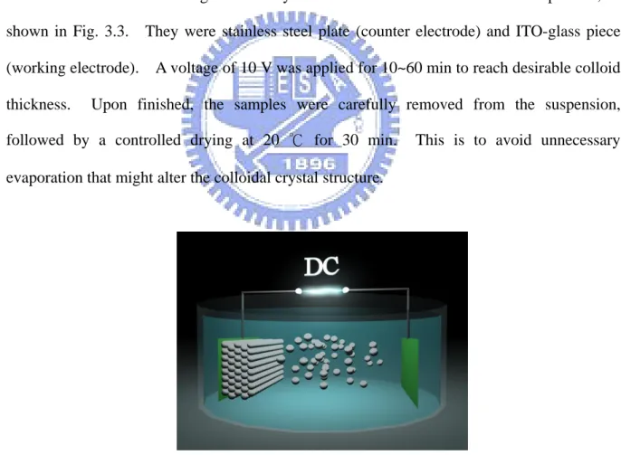
Two electrodes were arranged vertically at a distance of 10 mm for the EPD process, as shown in Fig. 3.3. They were stainless steel plate (counter electrode) and ITO-glass piece (working electrode). A voltage of 10 V was applied for 10~60 min to reach desirable colloid thickness. Upon finished, the samples were carefully removed from the suspension, followed by a controlled drying at 20 ℃ for 30 min. This is to avoid unnecessary evaporation that might alter the colloidal crystal structure.
Figure 3.3 A schematic diagram of experimental setting for the planar EPD process.
bunch of CFs (TORAYCA-T300). Then, they were pre-cleaned with DI water and degreased in acetone under ultrasonication. Subsequently, a segment of copper tape with silver colloidal gel was employed as a conductive cladding to fix the CF. Afterward, the as-prepared sample was further heated in oven at 50 ℃ to achieve complete dehydration. Next, the sample was cut into length of 1.5 cm to proceed EPD.
3.2.4 Fabrication of Cylindrical Colloidal Crystals
The EPD was carried out with two electrodes arranged vertically in a co-axial configuration. An as-prepared CF sample was immersed into the suspension at 1 cm depth. A stainless steel (A304) in circular shape was used as the counter electrode, as presented in Fig. 3.4.
Figure 3.4 A schematic diagram of experimental setup for the cylindrical EPD process.
A voltage of 10 V was applied to drive the EPD, and the distance between the counter and working electrodes was 2.3 cm. The assembly process lasted 0-60 min. When finished, samples of CCC were removed and kept at 20 ℃ for 10~20 min to evaporate ethanol slowly.
3.3 NED for Inverse Opals
3.3.1 Preparation of Electrolyte
The electrolyte for the nickel electrodeposition included NiSO4•6H2O (130 gL-1),
NiCl2•6H2O (30 gL-1), H3BO3 (18 gL-1), and H2O2 (3 mLL-1). A minute amount of H2SO4
and NaOH were added to adjust the pH value of the electrolyte. In addition, the solution was stirred for 1 day before electroplating, and raised to 45℃ prior to the NED process.
3.3.2 Fabrication of Inverse Opals
To fabricate Ni inverse opals, planar and CF substrates underwent similar EPD process in different PS suspensions with various processing variables. Before the electrodeposition, samples were immersed in the plating electrolyte with moderate stirring for 1 hr, and a hotplate coupled with a thermal couple was employed to control the temperature of the system. Next, the electrodeposition was carried out on EPD-derived colloidal crystals under an applied voltage of 1 V at 45 ℃ in electrolyte of pH 5.2. Upon finished, the samples were cleaned with DI water and dehydrated in oven at 50 ℃ for 1 hr. Table 3.1 provides relevant processing variables in the fabrication process. Current output was recorded with a Keithley 2400 during the NED process.
Table 3.1 EPD parameters of samples for sequent NED process.
Particle Size PS-460 PS-660 Concentration 2.5 gL-1 10 gL-1
Shape Planar Cylindrical Planar Cylindrical
Substrate Size 5×5 mm2 7×10⁻² π-mm2 15×15 mm2 7×10⁻² π-mm2
Electric Field/
Applied Voltage 15 V/cm 10 V 10 V/cm 10 V EPD Time 7.5 min 30 sec 30 min 45 sec
3.4 Removal of Polystyrene Template
3.4.1 Chemical Dissolution
PS microspheres after the NED process were carefully etched away by immersing the samples in an ethyl acetate (95 wt%) solution. The color for the sample would immediately change from white to purple/red as the solution percolated throughout the structure, making a larger contrast in the refractive index. After 2 days, the remaining Ni skeleton was cleaned with ethanol several times until the odor of ethyl acetate was removed. At this stage, we successfully made the Ni inverse opals.
3.4.2 Thermal Oxidation
PS microspheres were directly removed by a thermal oxidation treatment at temperatures of 250 ℃, 350 ℃, and 450 ℃ for 2 days. It is noted that the Tg (glass transition temperature)
and Tm (melting point) of PS are 95 ℃ and 240 ℃, respectively. Upon finished, the samples
were kept in oven for furnace cooling in order to avoid undesirable thermal distortion of the inverse structure.
3.5 Instrument
3.5.1 Morphological Observation
Scanning Electron Microscope (SEM)
A SEM (JEOL-LSM-6700) was employed to observe relevant morphologies for colloidal crystals and inverse opals. In SEM sample preparation, the specimens were mounted on a copper holder, while sputtering of Pt was carried out at 20 mA for 90 sec (for insulating samples) or 40 sec (for conductive samples). Afterward, the SEM specimens were maintained under a pressure of 9.63×10⁻⁵ Pa, and observed with an acceleration voltage of 15 kV and an emission current of 10 μA.
Optical Microscope (OM)
With light incidence directly normal to the sample surface, the OM (Olympus CX41) was used to observe the light diffracting from cylindrical colloidal crystals. The images were captured by a coupled digital CCD camera (CY-100A).
3.5.2 Characterizations
Energy Dispersive X-ray (EDX)
EDX attached on a SEM was used to perform the semi-quantatative composition report and elemental mapping for the inverse opals.
High Resolution X-ray Diffractometer (HRXRD)
A HRXRD (Bede D1) was used to determine the crystallinity and relevant composition for the nickel inverse opals before and after thermal treatments.
Keithaley 4200 to obtain the conductivity for the planar nickel inverse opals. For cylindrical nickel inverse opals, samples were fixed on a non-conductive glass with two silver bumps serving as the probe contact points, and a forward bias of 0~400 mV was applied during the measurement.
UV-Vis-IR Spectrum
Optical response for the colloidal crystals and their inverse opals were acquired through a Fourier Transform Infrared (FTIR) microscope (Hyperion 2000, Bruker) in a nitrogen atmosphere. During the measurement, the samples were illuminated with a selective light source (CaF2), and the reflectance was obtained by normalizing the measured signals detected
Chapter 4
Results and Discussion on EPD Process
This chapter provides the results and discussion on fabrications of colloidal crystals by the EPD in various processing parameters. Variables under studies were suspension concentration, applied electric field, and deposition time. In general, the deposit weight from an EPD process is expressed in equation 4.1 and 4.2 for planar and cylindrical cases, respectively [11];
𝑌 =
2 3𝐶
𝑠∙ 𝑆 ∙ 𝜀 ∙ 𝜉 ∙
1 𝜂∙
𝑉 𝐿∙ t
[eq. 4.1]𝑌 =
3𝑙𝑛(𝑎/𝑏)𝜂𝑙𝑉𝐶𝑠𝜀𝜉𝑡[eq. 4.2]
In equation [4.1], Y is the deposited weight of EPD layer, Cs is the mass concentration of
PS microspheres in suspension, S is the area of substrate, ε and ξ are the dielectric constant and zeta potential of PS microspheres, η is the viscosity of solvent in suspension, V is the applied voltage, L is the distance between working and counter electrodes, and t is the deposition time. In equation [4.2], there are three more variables in cylindrical EPD system;
l and a are the length and radius of the working electrode, and b is the radius for the coaxial
counter electrode (b > a). In this work, suspensions made of 460 and 660 nm PS microspheres (PS-460 and PS-660) were prepared in different Cs and examined to achieve a
smooth EPD coating. By driving the EPD process with suitable applied voltage (electric field), the planar and cylindrical colloidal crystals (PCC-460/660 and CCC-460/660) were successfully fabricated. The following sections provide detailed discussion on individual variables and their effects on the quality of colloidal crystals.
4.1 Suspensions and Substrates
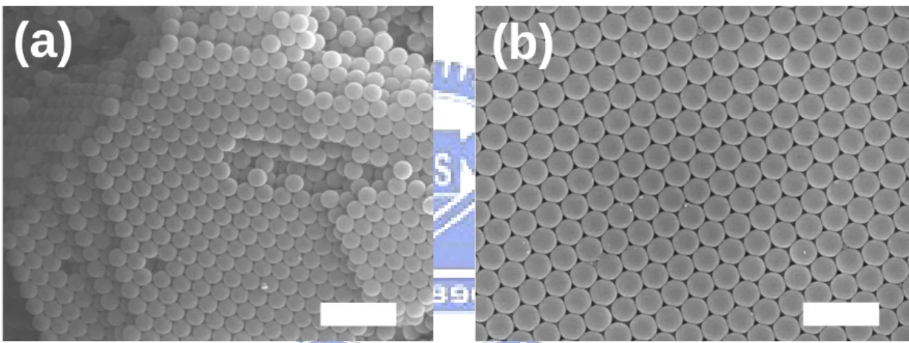
The as-synthesized PS microspheres are demonstrated in Fig. 4.1. The larger ones exhibited a diameter of 660 nm with a standard deviation of 16.4 nm while the smaller ones revealed a diameter of 460 nm with a standard deviation of 10.1 nm. Assembly of PS microspheres could be easily achieved simply by solvent evaporation. As shown, we obtained reasonable uniformity in size distribution and this attribute was critical for our EPD process. The PS microspheres were further mixed with ethanol to prepare the suspensions, PS-460 and PS-660.
Figure 4.1 SEM images of PS microspheres with diameter of (a) 460 nm and (b) 660 nm. The scale bars are 2 μm.
Figure 4.2 presents the plots of electrophoretic mobility in PS-460 and PS-660. Their concentrations were 2.5 g/L and 10 g/L, respectively. The mobility for the PS microspheres in each suspension appeared in a single peak with corresponding zeta-potential was above 60 mV. Both results suggested that our suspensions were in excellent stability and the size of PS microspheres was reasonably mono-dispersive.
Figure 4.2 Electrophoretic mobility of suspension (a) PS-460 and (b) PS-660.
4.1.1 Microsphere Concentration in Suspensions
While the PS microspheres were driven to deposit on the substrate from bulk suspension, it took some time to assemble them into a desirable close-packed arrangement. It is necessary for the first layer to be close-packed before the second layer can be deposited. Therefore, a reduced deposition rate was considered critical in fabricating high-quality colloidal crystals. After rearranging those variables in equation 4.1, we could derive that the Cs is proportional
to the deposition rate (Y/t). Thus, the Cs plays significant influence over the quality of the
colloidal crystals.
Figure 4.3 presents the SEM images of EPD layers fabricated in PS-460 with Cs of 10 g/L
and 2.5 g/L under 10 V/cm. As clearly shown in Fig. 4.3(a), the PS microspheres were in random arrangement with approximate domain size in 2~3 μm. In addition, a number of voids was observed among particles. When we reduced the PS microsphere concentration to 2.5 g/L, the domain of colloidal crystals became larger, as exhibited in Fig 4.3(b). These behaviors suggested that the EPD fabrication with an excess Cs could not deliver high-quality
colloidal crystals. Moreover, increase in the Cs enhanced the volume fraction of PS
microspheres, which raised op the viscosity of suspension and zeta potential. Thus, a larger Cs not only rendered a faster deposition rate but also affected the Brownian motion among
Figure 4.3 SEM images of EPD layers prepared in PS-460 with various microsphere concentrations of (a) 10 g/L and (b) 2.5 g/L. The electrical field was fixed at 10 V/cm for 3 min. The scale bars are 3 μm.
Identical experiments were also performed in PS-660 suspensions, with their results presented in Fig. 4.4. Similarly, the suspension of 10 g/L demonstrated a better quality in colloidal crystals over 25 g/L one. Howerer, this great difference in the optimized PS microsphere concentration between PS-460 and PS-660 suspension was resulted from their distinct volume fraction.
Figure 4.4 SEM images of EPD layer made in PS-660 with microsphere concentrations of (a) 25 g/L and (b) 10 g/L. The electrical field was fixed at 10 V/cm for 10 min. The scale bars
(a)
(b)
the values for electrophoretic mobility in PS-460 (2.5 g/L) and PS-660 (10 g/L) were almost the same, as shown in Fig. 4.2. This suggested that the stability of suspension was more relevant to the volume fraction but not mass fraction. Therefore, in following experiments we chose the 2.5 g/L of PS-460 and 10 g/L of PS-660 to fabricate colloidal crystals.
4.1.2 Shape of Substrates
Figure 4.5 exhibits the SEM images of EPD layers on planar ITO glass and carbon fiber prepared under 10 V in 0.25 g/L PS-460. The EPD layer on the ITO glass revealed a (111) plane in FCC lattice. In contrast, a defective structure was observed in the EPD layer on CF. We surmised that linear defects and curved surface of the CF might convert the state of arrangement from close-packed structure into a non-close-packed one. In the insets of Fig. 4.5, the thickness of ITO layer was 200 nm, and the diameter of CF was about 7 μm. In cylindrical case, the diameter size of the CF (7 μm) was only 10~15 times larger than that of PS microspheres (460 nm and 660 nm). Namely, EPD process was carried out on this curved surface (CF) with PS microspheres assembly, leading to a disordered EPD layer.
Figure 4.5 SEM images of EPD layer on (a) ITO glass and (b) carbon fiber. The insets provide the SEM images of each substrate. The scale bars are 5 μm in the figure and 2 μm in the inset.
4.2 Fabrication of Planar Colloidal Crystals (PCCs)
4.2.1 Electric Field in EPD process
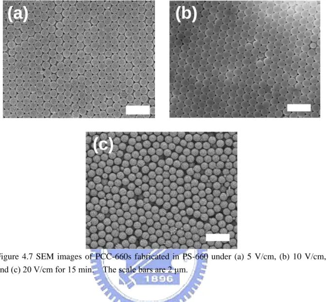
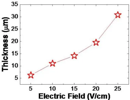
Figure 4.6 provides the thickness of PCC-660 made of various electric fields for 15 min on ITO glasses. The deposit thickness was linearly increased when the electric field was larger than 10 V/cm. However, a reduced deposition rate was present at 5 V/cm, which suggested that there was a transition regime for EPD rate between 5 V/cm and 10 V/cm.
Figure 4.6 Thickness versus electric field for the colloidal crystals made of PS-660. The EPD fabrication time was 15 min.
Figure 4.7 displays the SEM images for the colloidal crystals from 5 V/cm, 10 V/cm, and 20 V/cm, respectively. The PS microspheres were in close-pack structure at 5 V/cm, and became disordered as the applied electric field was increased. This suggested a larger driving force would engender a defective assembly. It is also known that a large electric
Figure 4.7 SEM images of PCC-660s fabricated in PS-660 under (a) 5 V/cm, (b) 10 V/cm, and (c) 20 V/cm for 15 min. The scale bars are 2 μm.
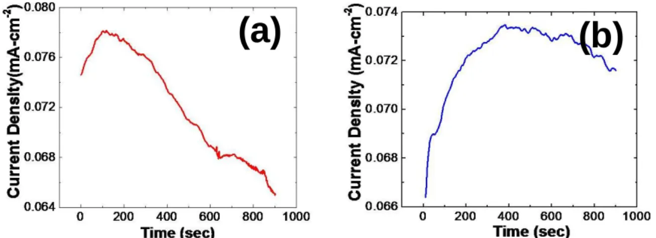
The thickness of EPD layer as a function of electric field using the 460 nm microspheres is displayed in Fig. 4.8. It was observed that the thickness of PCC-460 was linearly increased with the electric field. Figure 4.9 provides the SEM images for the samples made of 10 V/cm, 15 V/cm, and 25 V/cm, respectively. As expected, a larger electric field rendered a relatively disordered structure. Therefore, to improve the quality of PCCs, the electric field should be moderately reduced. Hence, we selected 15 V/cm in the EPD process using PS-460. Figure 4.10 demonstrates the relationship between current density (j) and deposition time (t) under the selected electric fields in PS-660 and PS-460. Both j-t curves reveal a decreasing current density at extended deposition time. This behavior indicated that the PS microspheres were self-assembling on the ITO glass, producing a mask to shield the
(a)
(b)
Figure 4.8 Thickness versus electric field for the colloidal crystals made of PS-460. The EPD fabrication time was 10 min.
(a)
(b)
Figure 4.10 Evolution of current density vs. time during the EPD process under (a) 10 V/cm using PS-660 microspheres and (b) 15 V/cm using PS-460 microspheres.
4.2.2 Deposition Rate for Planar EPD
Figure 4.11 demonstrates the plot of thickness versus time for the samples prepared in the EPD process.
Figure 4.11 Thickness versus EPD time for the PCC-660 (■) and PCC-460 (☆). The applied electric field was 10 V/cm in PS-660 and 15 V/cm in PS-460.
The estimated deposition rates were 1.064 μm-min-1 and 1.337 μm-min-1 for the PCC-660 and PCC-460, respectively. As clearly shown, the growth of PCCs was slowing down with
the EPD time. We attributed this phenomenon to the decreasing electric field as the PS microspheres assembled on the substrate. Figure 4.12 and 4.13 exhibit the SEM images for the samples prepared in the EPD process with the optimized parameters. As expected, the microspheres were assembled properly to form colloidal crystals in multiple layers.
(a)
(b)
(c)
(e)
(d)
Figure 4.13 SEM images of PCC-460s fabricated under 10 V/cm for (a) 2.5, (b) 5, (c) 7.5, (d) 10, and (e) 15 min, respectively. All scale bars are 5 μm.
(a)
(b)
(c)
(d)
4.3 Fabrication of Cylindrical Colloidal Crystals (CCCs)
4.3.1 Applied Voltage in EPD Process
As shown in equation 4.2, the yield amount from the cylindrical EPD process was modified by additional three parameters, a, b, and l, and it was further reduced by a constant about 8.79 (ln(a/b)) from that of planar EPD process. On the other hand, the applied voltage (V) was present in the equation as an independent parameter. Hence, we only controlled the voltage in the cylindrical EPD process.
Figure 4.14 display the SEM images of CCC-460s made from two different voltages in PS-660 for 30 sec. The morphology for the CCCs revealed a defective packed structure, which was resulted from the curved CF surface, as shown in Fig. 4.14(a). The diameter of CCC made of 5 V was about 9 μm, which was equal to 3 EPD layers. At this stage, the color of substrate remained dark, which can be easily observed by naked eyes.
In contrast, as shown in Fig. 4.14(b), the diameter of sample made of 10 V was about 60 μm, which was almost 30 layers. Because the size of CF was in micron range, its dimension was relatively small compared with the planar substrates. Therefore, under identical yield amount, the EPD layer prepared on the CF would be 103-104 times thicker as opposed to that of planar substrate. As a result, the effect of voltage during the EPD became extremely critical in the cylindrical case.
Figure 4.15 provides the diameter of CCCs under different applied voltages in the PS-460 and PS-660. Obviously, a voltage of 5 V was not able to deposit large amount PS microspheres in a short time, but 10 and 20 V were capable of delivering a much enhanced deposition rate for both PS-460 and PS-660 suspensions.
Figure 4.14 The SEM images of CCC-460s made of (a) 5 V, and (b) 10 V. The fabrication time was 30 sec. The scale bars are 5 μm in (a) and 10 μm in (b).
Figure 4.15 Diameter versus voltage for the CCC-460s (☆) and CCC-660s (■). Their fabrication time was 30 sec.
Figure 4.16 presents the SEM images of CCCs made of 10 V and 20 V by PS-660 and PS-460. Among them, the applied voltage of 20 V rendered a poor packing quality in the EPD layer because unnecessary larger EPD rate. In contrast, the 10 V exhibited a relatively dense packing in both suspensions. Because the diameter for the CCC-460 made of 10 V was much larger than that of CF, its fabrication could be approximated to a planar EPD case. Hence, the crystal quality of CCCs made of 10 V was still reasonable even the EPD rate of 10
V was much larger than that of 5 V. In addition, the CCC-460 revealed a better quality than that of 660 nm, as shown in Fig. 4.16(a) and Fig. 4.16(c). This suggested that the ratio of microsphere size to the diameter of substrate plays a critical role in desirable ordered arrangement. Hence, difference in the diameter for the CCCs indicated the importance of applied voltages. However, it was challenging to control the layer numbers with a large voltage because the deposition rate for the cylindrical EPD was taking place too fast.
Figure 4.16 SEM images on the surface morphology of CCC-660 made of (a) 10 V and (b) 20 V, as well as CCC-460 made of (c) 10V and (d) 20V. The fabrication time was 30 sec, and the scale bars are 5 μm.
(a)
(b)
and the self-assembling of PS microspheres was easy to be achieved. Hence, we selected the 10 V in following experiments
Figure 4.17 Time dependence of current density for (a) CCC-660 and (b) CCC-460 during cylindrical EPD process. The applied voltage was fixed at 10 V.
4.3.2 Deposition Rate for Cylindrical EPD
Figure 4.18 presents the plot of diameter versus time plots for the cylindrical colloidal crystals in the EPD process with PS-460 and PS-660. The diameter of CCC was linearly increased with deposition time, and a higher deposition rate was obtained in PS-440 than that in PS-660. Their respective deposition rates for the CCC-460 and CCC-660 were 0.322 μm-s-1
and 0.301 μm-s-1 intially, following by a slightly decrease to 0.201 μm-s-1 and 0.145 μm-s-1
after 6 min. These reduced rates indicated that those microspheres were arranged in proper packing order, reducing the pathway for the current on the substrate. According to the modified Hamaker’s equation [51] for cylindrical EPD, the linear dependence indicated our experiment was still in the primary stage of EPD. This suggested that the deposits could be further thickened in a short time.
Figure 4.18 Diameter versus EPD time for the CCC-660 (■) and CCC-460 (☆) fabricated in suspensions under a voltage of 10 V.
Figure 4.19 displays the SEM images for the CCC-660 made of 10 V in PS-660 for different EPD time. Microspheres in size of 660 nm were not stacking well on the CF first, but ordered layers were observed later and became FCC (111) plane, as shown in Fig. 4.19(a) and 4.19(b). It suggested that as the diameter of CCCs increased, the disorder region could be compressed and became the grain boundaries distributed in the close packed structure. If the deposition time was further prolonged, there were some BCC grains obtained in the EPD layers, as exhibited in Fig. 4.19(c). This indicated that the most stable state was not present by self-assembly on the carbon fiber substrate. There might be two reasons to explain the appearance of planes such as FCC (100) and BCC (100).
The first plausible cause is the undesirable high EPD rate. It is known that the EPD rate increased with deposition time within 10 min. Hence, a higher EPD rate would raise the
planes would reveal a non-close packed structure, or the BCC (100). This implied the EPD on a curved surface might be useful to achieve a defective packing structure. Figure 4.20 presents the SEM images of CCC-460 made of 10 V for various time in PS-460. Similarly, the size of ordered domains was becoming larger with the EPD time. However, the BCC plane was not found in the EPD layers.
Figure 4.19 SEM images for the surface morphology of CCC-660s made of 10 V in PS-660 for (a) 2 min, (b) 4 min, and (c) 8 min, respectively. All scale bars are 5 μm.
(a)
(b)
Figure 4.20 SEM images of the surface morphology of CCC-460s made of 10 V in PS-460 for (a) 2 min, (b) 4 min, and (c) 8 min. All scale bars are 5 μm.
Figure 4.21 presents the time dependence plot for the diameter of CCCs within 1 hr. From this figure, the increase in diameter of CCCs tended to reach a stable state after certain time. As pointed with arrows in the figure, a higher growth rate of CCCs was occurring after 30 min. The abnormal increase might be accidentally induced by “dip-coating” during sample removal.
(a)
(b)
Figure 4.21 Diameter versus EPD time for the CCC-660 (■) and CCC-460 (☆) fabricated in suspensions under a voltage of 10 V.
Figure 4.22 and 4.23 present the photographs of CCCs taken by an optical microscope. Both CCC-460 and CCC-660 exhibited smooth surfaces along the longitudinal axis, and the diameter for each sample revealed rather impressive uniformity. Therefore, for every sample, a direct reflectance was observed in the middle of CCC, and its intensity was enhanced when its diameter was increased under identical light source.
In optical response, the CCC-460 displayed a set of light diffracting fringes as the EPD process was extended longer, as shown in Fig. 4.22. These diffracting lines demonstrated a distribution of the reflective light in illumination with various angles on FCC (111), and the wavelength of reflectance increased from substrate to the surface due to increasing lattice spacing. However, there is no obvious light reflecting when the CCC-660 was illuminated by a white light, as exhibited in Fig. 4.23(a) and 4.23(b). The self-arranged layer of PS-660 was essentially distorted by a curved substrate and the size incoherence between substrate and spheres, as well as those linear defects on the CF.
Figure 4.22 Optical microscopy images of CCC-460 self-assembled in PS-460 for (a) 10 min and (b) 50 min. The scale bars are 200 μm.
Figure 4.23 Optical microscopy images of CCC-660 self-assembled in PS-660 for (a) 10 min, (b) 30 min, and (c) 50min, respectively. The scale bars are 200 μm.
(a)
(b)
(c)
So far, we have demonstrated that in fabricating the CCCs in a fixed diameter, smaller microspheres were easier to assemble. We observed that the CCC-660 was strongly affected by the substrate. For example, a pale rainbow color appeared on the CCCs with a longer EPD time, as shown in Fig 4.23(c). In short, the EPD process could deliver cylindrical colloidal crystals in a short period, and the applied voltage was optimized with the time dependence of current density. Furthermore, with a high EPD rate and curved surface, self-assembling of PS microspheres on a cylindrical electrode was capable of producing colloidal crystals with defective arrangements. More details from optical observation will be discussed in following sections.
Chapter 5
Results and Discussion on NED and PS Removal Processes
This chapter provides the results and discussion for NED and PS removal process in nickel inverse opals fabrication. In the NED process, a potentiostatic electrodeposition technique was carried out on the colloidal crystals to fabricate nickel inverse opals (NIO-460 and
NIO-660) and cylindrical inverse opals (CIO-460 and CIO-660). Figure 5.1 provides the
SEM images for those inverse opal structures. To remove colloidal PS templates, the as-prepared samples were treated under different temperatures in chemical dissolution or heat treatment.
Figure 5.2 presents the cross-sectional views for the as-prepared PCCs on ITO glass. The thickness of EPD layer for the PCC-460 and PCC-660 were 11.25 and 8.97 μm, respectively. As clearly shown in the figure, the PCCs were in good quality of proper stacking, and the PS microspheres demonstrated a three-dimensional close-packed arrangement.
Figure 5.3 displays the surface morphology for the as-prepared CCCs prior to the NED process. Clearly, the microspheres in the CCC-460 were in good order. In contrast, in the CCC-660, there revealed a defective packed structure. The insets exhibit the OM images for the as-prepared samples. The diameters were about 67.31 μm for the CCC-460 and 52.94 μm for the CCC-660, and these values were rather uniform along the longitudinal axis for both cases. It is noted that these colloidal templates were rather robust as immersing them in electrolytes did not produce unwanted detachments or structural damage.
Figure 5.2 Cross-sectional SEM images for the (a) PCC-460 and (b) PCC-660 before NED process. The scale bars are 5 μm.
Figure 5.3 SEM images on the surface morphology of (a) CCC-460 and (b) CCC-660. The scale bars are 5 μm. Insets display optical microscopic images for CCCs with scale bars of 100 μm.
5.1 Fabrication of Planar Nickel Inverse Opals
5.1.1 Current Density in NED Process
Figure 5.4 demonstrates the time dependence of current density during the NED process on planar colloidal templates. The value for current density exhibited a sudden jump initially and fluctuated with a positive slope subsequently. Previously, the current variation was used to derive the number of layer for the as-deposited inverse opal [50]. Accordingly, the PS microsphere on the substrate served as a mask that screened the current density.
Figure 5.4 Time dependence of current density during the Ni electrodeposition at pH of 5.2 and 1 V on PCC-460 (red) and PCC-660 (black). The inset plot shows the transition points that were determined by the variation of current density at initial stage. Inset axes are identical with the principal plot.
From the plot, the first drop of current density was obtained at 25 and 70 sec for the PCC-460 and PCC-660, respectively. This indicated that the nickel was deposited on the substrate, and became thicker until filling the cone-like interstitials. Hence, it took about 25 and 70 sec in the NED process for the NIO-460 and NIO-660 to grow into their semi-layers. The positive slope was recorded in the current density, which means the supply of nickel ions
increase in current density was resulted from the increased conductivity of electrode, because the nickel was deposited.
The XRD patterns for the NIO-660 and NIO-460 in multiple layers are exhibited in Fig. 5.5. The diffraction peaks in Fig. 5.5(a) confirmed a FCC structure with a preferred orientation of (111). The remaining two unmarked small peaks came from the substrate. The peaks from the substrates were also obtained in the plot of NIO-460 (Fig. 5.5(b)). The obvious noise from Fig. 5.5(b) indicated that its crystallinity was not as good as that of NIO-660. It is noted that the NIO-460 revealed only one characteristic peak in (111) plane. This suggested that formation of (200) and (220) planes was suppressed by physical confinement of the colloidal mask. To observe the as-deposited NIOs, the PS templates were further removed and the details in process are discussed later. Figure 5.6 shows the SEM images of NIOs-460 and NIO-660. Because it was expected to be harder for the electrolyte to percolate into the PCC-460, the quality of PCC-460 was likely to be maintained and improved over that of PCC-660. The insets in Fig. 5.6 exhibit the cross-sectional view for the NIOs. The ordered structure confirmed the robustness of the colloidal crystals in the electrolyte.
Figure 5.6 SEM images of multi-domains in planar (a) NIO-660 (b) NIO-460. The insets exhibit the cross-section view of each sample. All scale bars are 5 μm.
After Ni electrodepositions, the inverse opals revealed a somewhat disordered structure that displayed several lattice arrangements simultaneously. Their top view SEM images are shown in Fig. 5.7. Figure 5.7(a) exhibits the structure with only one hole in each pore, which corresponds to a rhombohedral lattice with 1-fold symmetry. Presented in Fig. 5.7(b) is a structure with two holes in each pore. That corresponds to the (110) in FCC. Figure 5.7(c) demonstrates a structure of closed-packed (111) plane. Figure 5.7(d) displays a (100) plane of FCC lattice with four holes in each pore, revealing a 4-fold symmetry with square shape. We surmised that appearance of these lattice structures was due to the shearing of microspheres occurring during NED process. Because immediately after the EPD, the samples were removed from the suspension and inserted into the Ni plating electrolyte. These disturbances would likely to engender undesirable shift in close-packed plane that results in defective structure.
Figure 5.7 SEM images of different lattice arrangement in planar NIO-460;(a) Rhombohedral, (b) FCC-(110), (c) FCC-(111), and (d) FCC-(100). All scale bars are 2 μm.
5.1.2 Deposition Rate for Planar NED
Figure 5.8 presents the optical images of planar nickel inverse opals made of NED process for 30 min. Their color appeared in dark-rosy for the NIO-660 and grey-purple for the NIO-460. It is known that the color of NIOs was resulted from the contrast of refractive index between Ni and air. For example, the appearance of multi-layer NIOs would turn immediately dark when the ethanol was filled into the structure. The insets in Fig. 5.8 demonstrate the reflective color of the samples for semi-layer NIOs observed from different
![Figure 2.1 First hybrid band structure of photonic crystal in a face-centered arrangement [24]](https://thumb-ap.123doks.com/thumbv2/9libinfo/8701554.199260/20.892.149.788.314.904/figure-hybrid-band-structure-photonic-crystal-centered-arrangement.webp)
![Figure 2.3 A schematic illustration of the principle of the dielectric mirror for 1-D PCs [32]](https://thumb-ap.123doks.com/thumbv2/9libinfo/8701554.199260/21.892.136.784.449.899/figure-schematic-illustration-principle-dielectric-mirror-d-pcs.webp)