高介電常數材料二氧化鉿於金屬-絕緣體-金屬電容之研究
93
0
0
全文
(2) 高介電常數材料二氧化鉿於 金屬-絕緣體-金屬電容之研究 Investigation of High-K Material HfO2 on Metal-Insulator-Metal Capacitor 研 究 生:許修豪 指導教授:羅正忠 博士. Student : Shiou-Hau Hsu Advisor : Dr. Jen-Chung Lou. 國 立 交 通 大 學 電子工程學系. 電子研究所碩士班. 碩 士 論 文 A Thesis Submitted to Institute of Electronics College of Electrical Engineering and Computer Science National Chiao Tung University in Partial Fulfillment of the Requirements for the Degree of Master of Science in Electronic Engineering July 2006 Hsinchu, Taiwan, Republic of China. 中華民國 九十五 年 七 月.
(3) 高介電常數材料二氧化鉿於 金屬-絕緣體-金屬電容之研究 研究生:許修豪. 指導教授:羅正忠 博士. 國 立 交 通 大 學 電子工程學系. 電子研究所碩士班 摘 要. 對於金絕金電容而言,尺寸的微縮可以減少晶片的大小和 類比與射頻電路的成本。為了達到高電容密度與低漏電流密度 的目標,高介電係數材料的需求是必要的。金絕金電容是利用 濺鍍二氧化鉿和鉭組成。使用二氧化鉿當高介電係數材料的金 2. 絕金電容,電容密度高達 25.67fF/um 以及漏電流密度大約 3.5 -7. 2. ×10 A/cm 。 之後,我們討論沉積後退火對於金絕金電容的影響。發現 到元件的漏電流密度在做完通氧氣時沉積後退火會變小,電容 密度則是再作完通氮氣時沉積後退火會變大的結果。另外,我 們還討論表面電漿處理對金絕金電容的影響。發現到元件的電 容電壓係數會變小的特性。 I.
(4) The Integrated Investigation of High-κ Material Al2O3 Student:Shiou-Hau Hsu. Advisor:Dr. Jen-Chung Lou. Department of Electronics Engineering and Institute of Electronics National Chiao Tung University, Hsinchu, Taiwan. Abstract. Continuous down-scaling of the size of metal–insulator–metal (MIM) capacitors is required to reduce chip size and the cost of analog and RF ICs. The use of a high-k dielectric is the only way to achieve this goal, since decreasing the dielectric thickness to achieve high capacitance density degrades the leakage current. Metal-insulator- metal (MIM) capacitors are fabricated using sputtered HfO2 with Ta for top and bottom electrodes. A very high density of 25.67fF/um2 has been measured in metal–insulator–metal (MIM) capacitors which use high-k HfO2 the dielectric. The characteristics the MIM capacitors show the leakage current densities around 3.5×10⁻⁷ A/ cm2.. II.
(5) In this thesis, we discussed post deposition annealing (PDA) effects on MIM. The devices show leakage current reduces density after post deposition annealing (PDA) in O2 ambient and capacitance density increases after post deposition annealing (PDA) in N2 ambient. In addition, we discussed plasma process effects on MIM. The devices present smaller Voltage coefficient of capacitance (VCC) than the sample without plasma treatment.. III.
(6) 誌. 謝. 時間過得真快,兩年的研究所生活即將結束。首先,我要 感謝我的指導教授羅正忠博士。協助我正確的研究方法與專業 的教導,建立深厚的研究基礎,讓我受益良多。也特別感謝論 文口試委員連振炘教授、龔正教授給予論文指導與意見。 此外,感謝實驗室的兩位學長— 永裕以及世璋學長,是你 們在我遇到困難及問題時,適時給予寶貴的意見,還有彥廷學 長對於本論文提供重要的意見,使其更加完整,謝謝你們! 在學業上,要感謝一起努力的同學們: 伯翰、文煜、國源、 建華、佳寧、致維、國信、忠樂……,在生活上,感謝:建廷、 永展、翰宗、鈞凱、志偉、昇霖、曜聲……,讓我在兩年的碩 士生活不至於枯燥乏味。也要感謝一傑、宏仁、彥銘、大峰、 智仁、……等學弟們的協助。 本論文獻給我最敬愛的父母許清恩先生、黃素英女士,感 謝他們多年來辛苦的栽培和養育,當我遇到困難的時候,給予 全力的幫助與支持,達成今日的成就,謝謝你們。還有我的姊 姊瑞玲、二哥修銘,謝謝你們跟我一起分享這兩年的點點滴滴, 最後,更要感謝女朋友素錦,陪伴我度過這些日子,謝謝你們。 另外,我要感謝國家奈米元件實驗室與交大奈米中心提供 良好的設備和每一位勞苦功高的工作人員所給予的幫助,讓我 能順利的完成實驗。謝謝! 這兩年回憶,是我和你們大家一起完成的故事,記錄在這 本論文裡。這本論文,獻給大家。謝謝你們~. IV.
(7) Contents Abstract (in Chinese)…………………………………………....Ⅰ Abstract (in English) ……………………………………..…….Ⅱ Acknowledgement…………………………………………........Ⅳ Contents…………………………………………………….........Ⅴ Table Captions…………………………….………………….....Ⅶ Figure Captions……………………………………….………...………Ⅷ. Chapter 1 Introduction…………………………………….…...1 1.1 Background…………………………………………………….……...1 1.2 Motivation……………………………………………………………..3 1.3 Organization of the thesis…………………………………...….……..7. Chapter 2 Characteristics of HfO2 Gate Dielectrics Deposited on Tantalum Meta………………..…………......12 2.1 Introduction…………………………………………………..….........12 2.2 Experiment Details……………………………………………..……..14 2.3 Results and Discussions…………………………..…………………..15 2.3.1 Basic Characteristics of HfO2 Dielectrics Deposited on Ta Metal …………………………………………………………….15. V.
(8) 2.3.2 Thermal Stress on the MIM Capacitors…………….………..…..19 2.3.3 J-V Curves Measurement under Various Temperatures………....20 2.3.4 Compared to MIM (TiN/Al2O3/TiN) and MIM (Ta/HfO2/Ta) structure………..………………………………………………..22 2.4 Summary…………………….……………………………………….23. Chapter 3 Characteristics of Al2O3 Gate Dielectrics Deposited on TiN Metal…………….………………………....37 3.1 Introduction…………………………….……………………….…...37 3.2 Experiment Details………………………………….……….……....38 3.3 Results and Discussions………………………….………….…….....39 3.3.1 Basic characteristic of the MIM with PDA Technology.…….....39 3.3.2. Basic. characteristic. of. the. MIM. with. Plasma. surface. Technology………………………………………………..…...41 3.3.3 Analysis Voltage coefficient of capacitance (VCC) on the MIM…….....................................................................................42 3.4 Summary……………………………..………..……..…...…….44. Chapter 4 Conclusions and Suggestions For Future Work….70 4.1 Conclusions……………………………………….….……………..…70 4.2 Recommendations for Future Works…………………..…..……..…..71. Reference…………………………………………….…….…....72 Vita……………………………………………………….….…..78 VI.
(9) VII.
(10) Table Captions Chapter 1 Table 1-1 Basic properties for many high-κ candidates [10].. Chapter 2 Table 2-1 Materials properties of high-κ dielectrics, Al2O3, ZrO2, and HfO2. Table 2-2 Summary of α and β extracted from MIM structure (Ta/ HfO2/Ta)) with 5nm. Table 2-3 Summary of Quadratic VCC, α, and linear VCC, β, extracted from MIM structure (Ta/HfO2/Ta) at 100 KHz for 5nm、6nm、9nm MIM capacitor.. Chapter 3 Table 3-1 Summary of Quadratic VCC, α and linear VCC, β extracted from MIM structure (Ta/HfO2/Ta) without and with 400°C、500°C in N2, 400°C、500°C in O2 PDA. Table 3-2 Summary of Quadratic VCC, α, and linear VCC, β, extracted from MIM structure (Ta/HfO2/Ta) without plasma and with N2O, NH3 plasma process for variant frequency. VIII.
(11) Figure Captions Chapter 1 Figure 1-1 The expected equivalent oxide thickness (EOT) trends from the published 2003- ITRS roadmap. Figure 1-2 Power consumption and gate leakage current density comparing to the potential reduction in leakage current by an alternative dielectric exhibiting the same equivalent oxide thickness [10]. Figure 1-3 DRAM cell structures for (a) planar type capacitor, (b) trench capacitor,and (c) stacked capacitor [11].. Chapter 2 Figure 2-1 Band alignment of topical high-κ dielectrics. Figure 2-2 Flow chart for the fabrication of HfO2 thin films. Figure 2-3 The C-V characteristics of the as-deposited HfO2 gate dielectrics for 5nm, 6nm, and 9nm were deposited difference thickness. Figure 2-4 Capacitance density varied with 5nm, 6nm, and 9nm HfO2 dielectric film thickness. Figure 2-5 (a) Capacitance-voltage (C-V) and (b) Capacitance-frequency characteristics of HfO2 5nm thin film on MIM capacitors at the frequencies from 1 kHz to 1 MHz. Figure 2-6 (a) Schematic representation of different mechanisms of polarization [22]. Figure 2-6 (b) Frequency dependence of several contributions to the. IX.
(12) polarizability [51]. Figure 2-7 (a) Normalized C-V curves (△C/Co) of MIM structure (Ta/ HfO2/Ta) with 5 nm thickness. Figure 2-7 (b) DC bias dependence of normalized capacitance (△C/Co) at 100 KHz for 5nm、6nm、9nm MIM capacitor. Figure 2-8 (a) Capacitance density of the MIM capacitor with 5nm thickness at 100 kHz from 25°C to 125°C. (b) Capacitance density of the MIM capacitor with 5nm thickness as a function of frequency after thermal stress from 25°C to 125°C. Figure 2-9 Capacitance density of the MIM capacitor as a function of temperature at frequencies varied from 100Hz to 1MHz. Figure 2-10 The J-V curves of MIM capacitor with 5nm thickness under various temperatures, ranging from 25°C to 150°C. Figure 2-11 Poole-Frenkel plot showing the current density versus electric field characteristics at five measurement temperatures from 25°C to 125°C for Ta/HfO2/Ta. Figure 2-12 Compared to the (a) C-V and (b) J-V curves of MIM structure (TiN/Al2O3/TiN) at 8nm and (Ta/HfO2/Ta) at 5nm.. Chapter 3 Figure 3-1 Flow chart for the fabrication of HfO2 thin films with PDA Technology. Figure 3-2 Flow chart for the fabrication of HfO2 thin films with Plasma Technology. Figure 3-3 The comparison of (a) and (b) C-V characteristics of MIM structure (Ta/HfO2/Ta) without PDA and with 400°C, 500°C ,. X.
(13) 600°C PDA in N2. Figure 3-4 The J-V curves characteristics of MIM structure (Ta/HfO2/Ta) without PDA and with 400°C, 500°C, 600°C PDA in N2. Figure 3-5 (a) and (b) AFM topography of HfO2/Ta structure without PDA. Figure 3-6 (a) and (b) AFM topography of HfO2/Ta structure with 400°C PDA in N2. Figure 3-7 (a) and (b) AFM topography of HfO2/Ta structure with 500°C PDA in N2. Figure 3-8 (a) and (b) AFM topography of HfO2/Ta structure with 600°C PDA in N2. Figure 3-9 the relationship between surfaces roughness relate to difference PDA temperature of HfO2/Ta structure. Figure 3-10 (a) and (b) C-V characteristics of MIM structure (Ta/HfO2/Ta) without PDA and with 400°C, 500°C, 600°C PDA in O2. Figure 3-11 the J-V curves characteristics of MIM structure (Ta/HfO2/Ta) without PDA and with 400°C, 500°C, 600°C PDA in O2. Figure 3-12 the relationship between capacitance densities relate to difference PDA temperature Figure 3-13 leakage current characteristics as a function of PDA temperatures with 400°C, 500°C and 600°C deposition in N2 and O2 Figure 3-14 the comparison of (a) C-V and (b) J-V characteristics of MIM structure (Ta/HfO2/Ta) without PDA and with N2O, NH3 plasma process on Ta electrode Figure 3-15 AFM topography of Ta bottom electrode without plasma process Figure 3-16 AFM topography of Ta bottom electrode with N2O plasma process, 600s Figure 3-17 AFM topography of Ta bottom electrode with NH3 plasma. XI.
(14) process, 600s Figure 3-18 the relationship between surfaces roughness relate to without and with plasma process on Ta electrode Figure 3-19 Normalized C-V curves (△C/Co) of MIM structure (Ta/HfO2/Ta) relate to without PDA and with 400°C、500°C PDA in N2 for 100 KHz Figure 3-20 Normalized C-V curves (△C/Co) of MIM structure (Ta/HfO2/Ta) relate to without PDA and with 400°C、500°C PDA in N2 for 10 KHz Figure 3-21 Normalized C-V curves (△C/Co) of MIM structure (Ta/HfO2/Ta) relate to without PDA and with 400°C、500°C PDA in N2 for 1 KHz Figure 3-22 Normalized C-V curves (△C/Co) of MIM structure (Ta/HfO2/Ta) relate to without PDA and with 400°C、500°C PDA in O2 for 100 KHz Figure 3-23 Normalized C-V curves (△C/Co) of MIM structure (Ta/HfO2/Ta) relate to without PDA and with 400°C、500°C PDA in O2 for 10 KHz Figure 3-24 Normalized C-V curves (△C/Co) of MIM structure (Ta/HfO2/Ta) relate to without PDA and with 400°C、500°C PDA in O2 for 1 KHz Figure 3-25 Quadratic VCC, α, versus difference frequency without PDA , with 400°C、500°C PDA in N2 and 400°C、500°C PDA in O2 Figure 3-26 Normalized C-V curves (△C/Co) of MIM structure (Ta/HfO2/Ta) relate to without plasma and with N2O, NH3 plasma process for 100 KHz Figure 3-27 Normalized C-V curves (△C/Co) of MIM structure (Ta/HfO2/Ta). XII.
(15) relate to without plasma and with N2O, NH3 plasma process for 10 KHz Figure 3-28 Normalized C-V curves (△C/Co) of MIM structure (Ta/HfO2/Ta) relate to without plasma and with N2O, NH3 plasma process for 1 KHz Figure 3-29 Quadratic VCC, α, versus difference frequency without plasma and with N2O, NH3 plasma process. XIII.
(16) CHAPTER 1 Introduction. 1.1 Background. The semiconductor device has a fairly long history, since that first IC (integrated circuit), circuit design has become more sophisticated, and the integrated circuit more complex. A single silicon chip may be on the order of 1 square centimeter and contain over a million transistors. Some ICs may have more than a hundred terminals,. while. an. individual. transistor. has. only. three.. Practical. metal-oxide-semiconductor (MOS) transistors were then developed in the 1960s. The MOS technologies, especially complementary metal-oxide-semiconductor (CMOS), have become a major focus for IC design and development. Silicon is the main semiconductor material [1]. MOS transistors can be made quite small, occupying a small silicon area on IC chip, and their manufacturing process is relatively simple, compared with bipolar junction transistor (BJT) manufacturing process. Furthermore, digital logic and memory functions can be implemented with circuits that use metal-oxidesemiconductor field effect transistor (MOSFET) only (that is, no resistors or diodes are needed). This is the reason why most very-large-scale integrated (VLSI) circuits are made at the present time using complementary metal-oxide-semiconductor (CMOS) technology, including microprocessor and memory chips. CMOS technology has also been applied extensively in the design of analog integrated circuits and in 1.
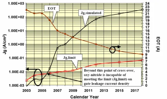
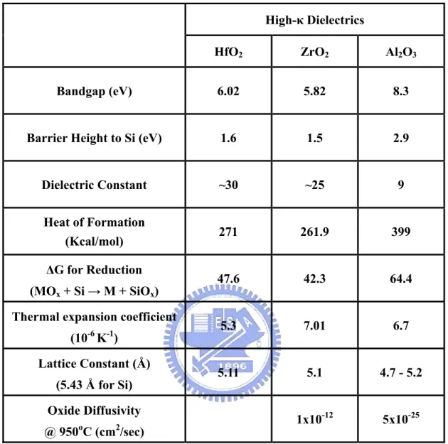
(17) integrated circuits that combine both analog and digital circuits. Since the 1980s, devices have been scaled such that performance doubled as the cost was cut in half every 2-5 years. This is the famous “Moore’s law”. The decrease of the dimensions of metal oxide semiconductor transistor has led to the need for alternative, high dielectric constant (κ) oxides to replace silicon dioxide as their gate dielectric. Silicon dioxide layers thinner than 1.6 to 2 nm have a leakage current over 1 A/cm2 due to direct tunneling through the oxide, which is too large for devices. As tunneling decreases exponentially with thickness, the tunneling current can be reduced by using thicker layers of high κ dielectrics, with the same equivalent capacitance or equivalent silicon dioxide thickness teq[2]. Figure 1-1 shows the expected equivalent oxide thickness (EOT) trends from the published 2003-ITRS roadmap (International Technology Roadmap for Semiconductor). It suggests that at the current rate of progress, we will need EOT of less than 2 nm by 2004, and oxy-nitrides can extend silicon dioxide (SiO2) limitation to 2006 without massive change in production technologies. After 2006, oxy-nitrides can not meet the limit on gate leakage current density. The scaling of MOSFET devices beyond 30 nm gate lengths will require alternative gate dielectrics instead of conventional silicon dioxide or oxy-nitrides. The problem of high gate leakage current and high power consumption become more severe as gate-oxide thickness are aggressively reduced. High-κ gate materials can maintain the same EOT with thicker physical thickness, and is therefore expected drastically reduced direct-tunneling current. From Figure 1-2, the increased physical thickness significantly reduces the probability of tunneling across the insulator, and hence, reduces the amount of off-state leakage current density [3]. The relationship between dielectrics constant and thickness is followed:. 2.
(18) EOT =. 3.9 × ε 0 × A Cm. k high−k =. [eq-1]. k ox × t high−k. [eq-2]. EOT. The continuing miniaturization of complementary metal-oxide-semiconductor (CMOS) devices requires gate insulators, the dielectric constants (κ) of which are larger than the vale of the conventionally used silicon dioxide. Example of such high-κ materials are aluminum oxide (Al2O3) [4], zirconium oxide (ZrO2) [5] [6], hafnium oxide (HfO2) [7] [8], tantalum oxide (Ta2O5) [9], Table 1-1 summarizes the properties of potential high-κ candidates. Among high-κ materials, HfO2 is one of the most promising candidates due to high κ (~25) and lager band gap (5.7 eV), HfO2 is suitable to be integrated into DRAM process. HfO2 is therefore chosen in this thesis. However, the crystallization temperature of HfO2 is quite low, which restricts the thermal budget after the deposition and brings about the high leakage current and non-uniformity associated with grain boundaries.. 1.2 Motivation. In the early age of DRAM development, two-dimensional cell structure was widely applied on the standard DRAM cell, known as the “planar type” DRAM, as shown in Figure 1-3(a). Memory cell capacitance plays a key role, which can determine the sensing signal margin, speed, data retention time and endurance against 3.
(19) the soft error. In the multimega bit generation, the minimum cell capacitance should be 25fF/cell. Capacitance can be described as the following equation.. C=ε0εrA/d. [eq-3]. where C: the dielectric capacitance. ε0: the vacuum permittivity εr: the relative dielectric constant of dielectric material A: the surface area of capacitor d: the dielectric thickness. In order to get high memory density and high capacitance in the DRAM chip, increasing the surface area of capacitor and the relative dielectric constant of dielectric material can be used to increase capacitance. Three-dimensional cell structure was introduced to 4Mb-above generation, trench capacitor cell and stacked capacitor cell (STC). Both of the trench and the stacked cell techniques are still used in commercial DRAM products now, but they have been greatly improved in the past several generations, as shown in Figure 1-3 (b) and (c) [11], [12]. Three-dimensional cell structure of DRAM increases the surface area of capacitor to get high capacitance, nevertheless, it is not enough if the device dimension keep shrinking. Improve the relative dielectric constant of dielectric material is another way to get high capacitance without the limitation of device dimension.. The dramatic increase in wired and wireless communications has triggered the demand on metal-insulator-metal (MIM) capacitors with low parasitic, high quality factor, and low voltage coefficients for radio frequency and analog/mixed-signal integration circuit applications [13]. Moving forward to address the objective of minimizing the capacitor area to increase the circuit density, it can be achieved by. 4.
(20) employing either thinner dielectric or high-dielectric-constant (high κ) dielectric materials. However, leakage current and reliability issues limit the aggressive dielectric thickness scaling down in the case of conventional SiO2 (κ~4) and Si3N4 (κ~7), and therefore high-κ materials are much preferred as a possible solution. There are a wide variety of films with higher κ values than SiO2, ranging from Si3N4 with a κ value of 7, up to Pb-La-Ti (PLT) with a κ value of 1,400. Unfortunately, many of these films are not thermodynamically stable on silicon, or are lacking in other properties such as a high breakdown voltage, low defect density, good adhesion, thermal stability, low deposition temperature, ability to be patterned easily and low charge states on silicon. Currently interest seems to be centered on films such as HfO2 with κ values of 25~30, enabling a 6.4x to 10.3x increase in film thickness for equivalent performance. Transistors based on these films showed excellent overall performance presenting possible solutions to the need for thinner EOT with low leakage. Therefore, HfO2 performs promising competitiveness due to its relatively high free energy of reaction with Si (47.6 kcal/mole at 727oC) [14], and relatively high band gap (~5.8eV) among the high-k contenders [15]. However, the crystallization temperature of HfO2 is quite low, which restricts the thermal budget after the deposition and brings about the high leakage current and non-uniformity associated with grain boundaries.. MIM capacitors with HfO2 dielectric have been investigated using different deposition techniques such as reactive sputtering, atomic layer deposition (ALD), and pulsed laser deposition. The dielectric Films produced by chemical vapor deposition and metal organic solution deposition must be produced at high temperatures and often contain carbon contamination from the metal organic precursor. CVD films 5.
(21) have better step coverage than sputtered films, but produce films that have less desirable mechanical and electrical properties such as high leakage current. Reactive sputtering has many advantages. For example, it is compatible with the other steps of microelectronic processing. Most importantly, DC sputtering is performed at relatively low temperatures. This allows for the deposition of amorphous films. The major drawback in sputtering, however, is the determination of process conditions to obtain stoichiometric films [16]. Reactive sputtering is a very important process in thin-film deposition particularly for manufacturing complex compound films such as oxides, nitrides or carbides. Due to their immense applications, the process is extensively used by the semiconductor and display industries. The introduction of a reactive gas creates a transition from metals to compounds (oxides, nitrides and carbides, etc.) in both the target and substrate. In the conventional MIS structure, metal/ insulator/ Si-substrate has been used for a long period. There are many studies about high-κ on Si-substrate. Comparing with SiO2, the most benefit for high-κ gate dielectrics is leakage current density reduction by several orders of magnitude at the same EOT. However, in device performance point of view, a suitable gate dielectric candidate should also meet the other requirements, such as high thermal stability, high carrier mobility, small oxide charges, and good stress immunity and CMOS compatible. Different from semiconductor (Si-substrate), metal has more carriers and is more conductive. Therefore, MIM structure (metal /insulator /metal) can reduce contact resistance and raise storage charge comparing to MIS structure. On the other hand, in the trench DRAM process, trench capacitor is made by MIS structure (Polysilicon/ high-κ/ n-type dopant Si). As DRAM density increasing, device shrinkage and higher charge. 6.
(22) storage is inevitable. It is hard for conventional MIS structure to meet the requirements, MIM structure is expected to apply in trench DRAM process. We are interested in this topic, and trying to apply MIM structure in trench DRAM process. Besides, we are wondering if high-κ material interacts with metal electrode. If high-κ material interacts with metal electrode, there will be an interfacial layer between high-κ material and metal electrode. That will change whole film property, such as interface roughness, interface stress, electron barrier height, and thermal stability, etc. These issues will be discussed as well.. 1.3 Organization of the Thesis. This thesis is comprised of four chapters. Chapter 1 describes the background and motivation for the high-κ dielectrics and application of the MIM structure. In Chapter 2, we first describe the experimental procedure and then, show the basic characteristics of HfO2 gate stacks on the metal of Tantalum (Ta), including basic analysis of the C-V, I-V and AFM characteristics. The HfO2 thin film in this thesis is deposited by Reactive sputtering (RS), and let us compare these results with the thin film of Al2O3 on TiN metal is deposited by metal-organic chemical vapor deposition (MOCVD). In Chapter 3, we analyze the PDA effect of different temperatures with HfO2 on Ta metal in oxygen (O2), nitrogen (N2). However, MIM structure performance is not as good as we expected. High leakage current density is fatalness of MIM structure after PDA over 500°C in nitrogen (N2). In addition leakage current density reduced after PDA in oxygen (O2). We found out plasma N2O or NH3 surface treatment for bottom electrode can improve value of Voltage coefficient of capacitance (VCC). 7.
(23) Finally, in Chapter 4, the conclusions are made and the recommendation describes the topics which can be further researched.. 8.
(24) Figure 1-1 The expected equivalent oxide thickness (EOT) trends from the published 2003- ITRS roadmap.. Figure 1-2 Power consumption and gate leakage current density comparing to the potential reduction in leakage current by an alternative dielectric exhibiting the same equivalent oxide thickness [10]. 9.
(25) Band gap Eg(eV). △Ec(eV). Material. Dielectric Constsnt(k). SiO2. 3.9. 8.9. 3.2. Amorphous. Si3N4. 7. 5.1. 2. Amorphous. Al2O3. 9. 8.7. 2.8. Amorphous. Ta2O5. 26. 4.5. 1-1.5. Orthorhombic. TiO2. 80. 3.5. 1.2. Tetrag.. HfO2. 25. 5.7. 1.5. Mono.,Tetrag.,Cubic. ZrO2. 25. 7.8. 1.4. Mono.,Tetrag.,Cubic. to Si. Crystal Structure(s). Table 1-1 Basic properties for many high-κ candidates [10].. 10.
(26) (a). (b). (c) Figure 1-3 DRAM cell structures for (a) planar type capacitor, (b) trench capacitor, and (c) stacked capacitor [11]. 11.
(27) CHAPTER 2 Characteristics of HfO2Gate Dielectrics Deposited on Tantalum Metal. 2.1 Introduction. A high capacitance density is important for a MIM capacitor to increase the circuit density and reduce the cell area and cost. Therefore, adoption of high-k material like Al2O3 or HfO2 is a very efficient way to increase the capacitance density. Silicon oxide and silicon nitride are dielectrics that are commonly used in conventional capacitors, but their capacitance densities are limited due to low dielectric constants. It is expected to be one solution to enhance the capacitance density by using higher dielectric constant materials. Among various high-k dielectric candidates, HfO2 has been investigated as a promising material in gate dielectric of MOSFETs due to its high dielectric constant, excellent thermal stability, and high band gap. In addition, excellent MOS capacitors with HfO2 have also been demonstrated. Therefore, it seems that HfO2 is a promising candidate for the above applications. The most commonly reported high-k materials are ZrO2, HfO2, La2O3, and Al2O3 and so on. The dielectric constants of reported high-k materials are listed in 12.
(28) Table 2-1[17]. Among these candidates, HfO2 attracts much more attention from recent researches. The reasons are briefly listed as follows.. (1) Suitable high dielectric constant: The reported dielectric constant κ of HfO2 is about 25 ~30. This magnitude of κ-value is higher than that of Si3N4 (κ~7) and Al2O3 (κ= 8~11.5). It is not high enough to induce severe FIBL effect.. (2) Wide bandgap: In general, as the dielectric constant increases, the bandgap decreases. The narrower bandgap would increase leakage current. The energy band offset of HfO2 is about 5.68eV, which is higher than the other high-κ materials such as ZrO2, Si3N4, and Ta2O5.. (3) Acceptable band alignment: Band alignment determines the barrier height for electron and hole tunneling from gate or Si substrate. For SiO2, the band offset of conduction band and valence band is ~9eV, and the barrier height for electrons is 3.5eV and the barrier height for holes is 4.4eV. The high band offset for both electron and hole has the benefit of low leakage current. Figure 1-1 shows the calculated band offsets for most high-k dielectrics. For HfO2, barrier height for electron and hole is 1.6ev and 3.4eV, respectively. This band alignment is acceptable and better than other high-k materials such as Ta2O5.. 13.
(29) (4) High free energy of reaction with Si: For HfO2, the free energy of reaction with Si is about 47.6 Kal/mole at 727 ℃,(see Table 2-1) [17] which is higher than that of TiO2 and Ta2O5. Therefore, HfO2 is a more stable material on Si substrate as compared to TiO2 and Ta2O5. [18]-[20]. (5) High heat of formation: Among the elements in IVA group of the periodic table (Ti, Zr, Hf), Hf has the highest heat of formation (271 kcal/mole). Unlike other silicides, the silicide of Hf can be easily oxidized. That means that Hf is easy to be oxidized to form HfO2 [18]-[20]. According to these profits above discussions, we choose HfO2 as the major high-k material and in our investigation. The measurement is performed by MIM capacitor structures.. 2.2 Experimental details. Four inches diameter (150-mm) p-type (100) Si wafers with nominal resistivity of 15 to 25 Ω-cm were used as substrate. Prior to the growth of Ta metal, the native oxide was cleaned by the conventional RCA cleaning and diluted HF etching in sequence for the removal of particles and native oxides. The capacitor area in this measurement about is 5.3×10⁻⁴ cm2. After standard RCA cleaning, a 550 nm SiO2 film was grown on Si substrate by wet oxidation, the 100 nm Ta layers were deposited sequentially by dc sputtering to obtain a Ta/SiO2/Si structure for the deposition of 14.
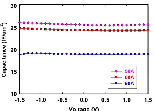
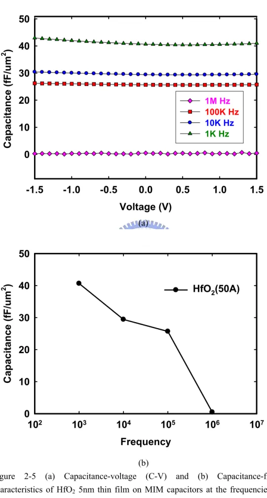
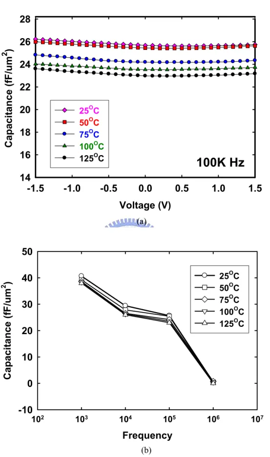
(30) HfO2 thin-film capacitors. After that, the HfO2 thin film of approximately different thickness for 5 nm, 6 nm, and 9 nm was deposited on Ta electrode. In addition, Bottom electrode is defined by mask. After HfO2 deposition, Ta gate was defined directly by metal mask. All these processes are performed at room temperature. Figure 2-2 shows the flow chart of HfO2 thin film fabrication. The physical gate oxide thickness was determined by n&k analyzer 1280. The equivalent oxide thickness (EOT) was extracted by fitting the measured high-frequency capacitance-voltage (C-V) data from Hewlett-Packard (HP) 4284LCR meter under zero-biased. Moreover the capacitance was measure using 4284LCR meter at frequencies varied from 1 kHz to 1 MHz. In order investigate the thermal stability of high-k dielectric film. Thermal stress was performed with measurement temperature varied from 25°C to 125°C. The tunneling leakage current density-voltage (J-V) was measured by semiconductor parameter analyzer HP4145A.. 2.3 Results and Discussions. 2.3.1 Basic Characteristics of HfO2 Dielectrics Deposited on Ta Metal. Figure 2-3 reveals The C-V characteristics of the as-deposited HfO2 gate dielectrics for 5nm, 6nm, and 9nm were deposited difference thickness. The capacitance density deposited at 9nm of film thickness was lower than 5nm deposited sample with similarly condition. When gate oxide film reduces, the capacitor density significantly shows high desired results. The Figure 2-4 clearly display the capacitance density at 5nm film thickness has 25.67fF/cm2. The capacitor dielectrics 15.
(31) with higher dielectric constant κ offer an attractive path to achieving enhanced capacitance per area. It should be pointed out here that high-κ use as a gate oxide is distinct from high-κ use in DRAM capacitors. As mentioned previously, HfO2 gate dielectrics exhibit high capacitance density and replace conventional SiO2. Since thinner HfO2 dielectric films would expect to have higher capacitance density than thick dielectric films. The corresponding capacitance-voltage (C-V) characteristics at the frequencies from 1 kHz to 1 MHz curves were presented in Figure 2-5 (a) (b). Figure 2-5 (a) (b) shows the frequency-dependence of the voltages of HfO2 dielectric films at 5nm samples. The capacitance densities reduced from 40.65fF/cm2 at 1 kHz to 25.67fF/cm2 at 100 kHz. However, the capacitance densities are very low at 1 MHz. The capacitance density decreases to about 0.47 fF/µm2 at 1 MHz compared to 40.7 fF/µm2 at 100 kHz. However, more serious frequency dispersion effect is shown in MIM. The capacitance densities decrease with increasing frequency in the range from 100 Hz to 1 MHz. It can be explained that at lower frequencies, we have different types of polarizations such as electronic polarization, orientation polarization, space charge polarization, and atomic polarization. Figure 2-2 shows the four types of polarizations.. These four compositions are illustrated as following. (1) Electronic polarizability, αe. Electronic polarization occurs in all dielectric materials. The electrons surrounding each nucleus are shifted very slightly in the direction of the positive electrode and the nucleus is very slightly shifted in the direction of the negative electrode. As soon as the electric field is removed, the electrons and nuclei return to their original distributions and the polarization disappears. The effect is. 16.
(32) analogous to elastic stress and strain. The displacement of charge is very small for electronic polarization, so the total amount of polarization is small compared to the other mechanisms of polarization. (2) Orientation polarizability, αo. Orientation polarization involves nonsymmetrical molecules that contain permanent electric dipoles. An example is H2O. The covalent bonds between the hydrogen and oxygen atoms are directional such that the two hydrogens are on one side of the oxygen. The hydrogen side of the molecule has a net positive charge and the oxygen side has a net negative charge. Under an electric field, the molecules will align with the positive side facing the negative electrode and the negative side facing the positive electrode. Orientation polarization results in a much higher degree of polarization than electronic polarization. This is because large charge displacement is possible in the relatively large molecules compared to the spacing between the electrons and nucleus in individual atoms. (3) Space charge polarizability, αs. Space charges are random charges caused by cosmic radiation, thermal deterioration, or are trapped in the material during the fabrication process. (4) Atomic or ionic polarizability, αi. It involves displacement of atoms or ions within a crystal structure when an electric field is applied. A wide range of polarization effects is possible through this mechanism, depending on the crystal structure, the presence of solid solution, and other factors. Examples include pyroelectricity, piezoelectricity, and ferroelectricity, Figure 2-6 (a) shows the four types of polarizations. At higher frequencies, the capacitance densities have main contribution from the electronic polarization [21]. Just as we have a relaxed and an unrelaxed elastic modulus, we have a dependence of the capacitance densities on frequency which shown in Figure 2-6 (b). The electronic 17.
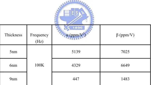
(33) polarization is the only process sufficiently rapid to follow alternative fields in the visible part of the spectrum. Ionic polarization processes are able to follow an applied high-frequency field and contribute to the capacitance densities at frequencies up to the infrared region of the spectrum. Orientation and space charge polarization have relaxation times corresponding to the particular system and process but, in general, participate only at lower frequencies. At Figure 2-5 (a) (b), the capacitance densities decrease with increasing frequency in the range from 100 Hz to 1 MHz. It can be explained that at lower frequencies, we have different types of polarizations such as electronic polarization, orientation polarization, space charge polarization, and atomic polarization. At higher frequencies, the dielectric constant has main contribution from the electronic polarization. Refer to Figure 2-6 (b), the capacitance densities decreases in the frequency ranging from 100 Hz to 1 MHz may be attributed to the decrease of space charge polarization.. Figure 2-7 (a) shows the normalized C-V curves (△C/Co) of MIM structure (Ta/HfO2/Ta). Voltage coefficient of capacitance (VCC) is one of the important parameters of MIM structure. It has been demonstrated that pure SiO2 MIM structures show negative parabolic curves in C-V relationship, but high-κ MIM structures exhibit strong positive parabolic curves in C-V relationship [40]. The mechanism of nonlinearity of C-V curves is unclear. It is supposed to relate with E-field polarization, carrier injections [23], high-κ thickness [24、25], frequency [26] and leakage current [27]. Theoretically, VCC decreases with measured frequency increases [24]. It is believed that the carrier mobility becomes smaller with increasing frequency, which leads to a higher relaxation time and a smaller capacitance variation [23]. From the equation below, where the voltage coefficients of capacitance (VCC) values of α and. 18.
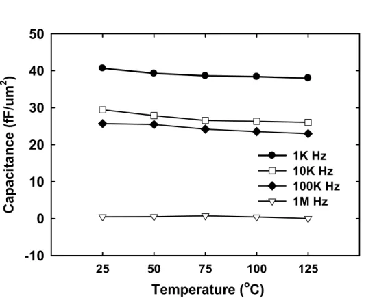
(34) β are listed in Table 2.2. The requirement of the quadratic coefficient of capacitance α is smaller than 100 ppm/V2, and the requirement of the linear coefficient of capacitance β is below 1000 ppm/V according to the ITRS roadmap [28].. dC C (V ) − Co = = αV 2 + β V + 1 Co Co Normalized capacitances (△C/Co) as a function of voltage with different thickness are shown Figure 2-7 (b) and Table 2.3. The decreasing of α with thickness is slower. This thickness effect is due to E-field reduction with increased thickness [47]. Thickness effect of the VCC is a negative impact for thinner film dielectric. 2.3.2 Thermal Stress on the MIM Capacitors. Figure 2-8 (a) depicts Capacitance density of the MIM capacitor with 5nm thickness at 100 kHz from 25°C to 125°C. Figure 2-8 (b) depicts Capacitance density of the MIM capacitor with 5nm thickness as a function of frequency after thermal stress from 25°C to 125°C. After thermal stress, the capacitance density decreases with temperatures at 100 kHz. The major reason is considered to be the interface defect density increasing during the thermal stress process. Moreover, the capacitance density decreases with frequency at all thermal stress. Especially, the capacitance density at 1 MHz is very lower than other frequency. As mentioned previously, the poorer frequency dispersion for MIM is probably decreased with space charge polarization. Figure 2-9 clearly confirms the results of Figure 2-8 (a) and (b).. 19.
(35) 2.3.3 J-V Curves Measurement under Various Temperatures. Figure 2-10 shows J-V characteristics of MIM capacitor measured at various temperatures from 25°C to 125°C. The dependence of leakage current density and measured temperature is observed, i.e. leakage current density increases with measurement temperature increased. Conduction mechanism is found by fitting equation described as follows. Many conduction mechanisms are fitted, including Fowler-Nordheim Tunneling [29、30] , Frenkel-Poole Emission [29、30], Trap Assisted Tunneling [31、32], and Schottky Emission [29]. In the Fowler-Nordheim Tunneling model, leakage current occurs in the high field region. High electric field across on high-κ thin film inclines band diagram and electron can tunnel more easily. The equation of leakage current density is [33]:. ⎡ − 4 2m* (qφ )3 / 2 ⎤ ⎛ b⎞ 2 B J = E exp ⎢ ⎥ ~ V exp⎜ − ⎟ 3qhE ⎝ V⎠ ⎣⎢ ⎦⎥ 2. The Fowler-Nordheim Tunneling plots were made for Jg (not shown in the thesis). In the Fowler-Nordheim Tunneling plots, Jg does not show a linearity relationship. The conduction mechanism is therefore not the Fowler-Nordheim Tunneling. In the Schottky Emission model, the Schottky emission is generated by the thermionic effect and is caused by the electron transport across the potential energy barrier at a metal-insulator interface. The equation of leakage current density is [33]:. (. ⎡ − q φ B − qE / 4πε I J = A*T 2 exp ⎢ kT ⎢⎣. )⎤⎥ ~ T. 2. ⎥⎦. 20. ⎛ + a V qφ B ⎞ ⎟ − exp⎜⎜ kT ⎟⎠ ⎝ T.
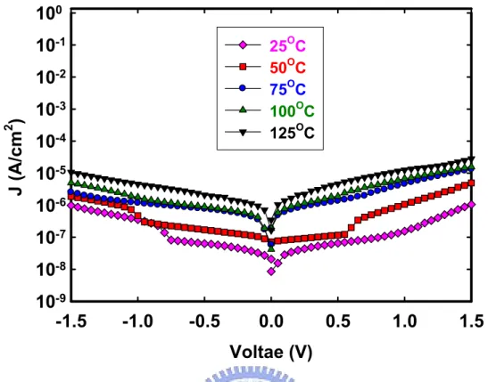
(36) The Schottky Emission plots were made for Jg (not shown in the thesis). Jg does not show a straight line in the Schottky Emission plots, therefore the conduction mechanism is probability not the Schottky Emission. In the Trap Assisted Tunneling model, it is assumed that electrons first tunnel through the SiOx interfacial layer (direct-tunneling). Then, electrons tunnel through traps located below the conduction band of the high-κ thin film and leak to substrate finally [31]. The equation of leakage current density is [32]:. J=. ⎡−β ⎤ exp ⎢ ⎥ Eox ⎣ EOX ⎦. α. The Trap Assisted Tunneling model plots were made for Jg (not shown in the thesis). Jg is not a straight line in the Trap Assisted Tunneling model plots, therefore the conduction mechanism is probability not the Trap Assisted Tunneling model. In the Frenkel-Poole Emission model, a lot of traps exist in high-κ thin film and electrons which get enough thermal energy can leap and stay in these traps temporarily and leak to substrate in the end. The equation of leakage current density is [33]:. (. ). ⎡ − q φ B − qE / πε I ⎤ ⎛ + 2 a V qφ B ⎞ ⎟ J = E exp ⎢ − ⎥ ~ V exp⎜⎜ ⎟ kT T kT ⎥⎦ ⎝ ⎠ ⎣⎢. The Frenkel-Poole Emission model plots were made for Jg in Figure 2-11. Jg shows a clear linearity in the Frenkel-Poole Emission model plots, therefore the conduction mechanism is probability the Frenkel-Poole Emission model.. 21.
(37) From the conduction mechanism fitting, we speculate that the conduction mechanism of MIM structure is Frenkel-Poole Emission.. 2.3.4 Compared to MIM (TiN/Al2O3/TiN) and MIM (Ta/HfO2/Ta) structure. Figure 2-12 (a) C-V curves depicts significantly the capacitance densities at TiN/Al2O3/TiN structure is lower than Ta/HfO2/Ta structure. Because the dielectric constants with HfO2 are higher than Al2O3, Ta/HfO2/Ta structure can increase the circuit density and reduce the cell area and cost. In addition, Figure 2-12 (b) shows Ta/HfO2/Ta structure performances better than TiN/Al2O3/TiN structure in leakage currents. In TiN/Al2O3/TiN structure, we found out that TiN might react with Al2O3 with high thermal budget resulting in inter-diffusion of Ti and Al. Lots of metal ion Ti in the Al2O3 thin film and incomplete structure of Al2O3 might be the reason of high leakage current density. Moreover, another reason is considered to be chlorine out-diffusion. In order to improve high leakage current density, we make attempt to different methods. e.g., we inserted AlN between Al2O3/TiN and deposited electrode thickness thinner. But these methods decrease defects insignificantly. Now we used another high-k material HfO2 and metal Ta instead of Al2O3 and TiN. CVD films have better step coverage than sputtered films, but produce films that have less desirable mechanical and electrical properties such as high leakage current. For some material we believe reactive sputtering is better than MOCVD, because reactive sputter product contamination less.. 22.
(38) 2.4 Summary. In this chapter, MIM capacitors have been successfully fabricated with HfO2 as the dielectric layer. We also discussed Characteristics of HfO2 Gate Dielectrics Deposited on Tantalum Metal. We found out the poorer frequency dispersion for MIM (Ta/HfO2/Ta) structure. Besides, the capacitance density under high frequency is very low, especially at 1 MHz. the voltage coefficients of capacitance (VCC) values of α and β are higher than 100 ppm/V2 1000 ppm/V according to the ITRS roadmap. Furthermore, conduction mechanism of Ta/HfO2/Ta structure has been studied. The conduction mechanism of Ta/HfO2/Ta structure is Frenkel-Poole Emission. The measurement results show high capacitance density compared to TiN/Al2O3/TiN structure. The Ta/HfO2/Ta capacitor exhibits the highest capacitance density value of 25.67fF/µm2. The leakage currents of Ta/HfO2/Ta capacitors are very small compared to TiN/Al2O3/TiN structure. These show that the HfO2 dielectric is very suitable for MIM applications. Thus indicates that it is very suitable for HfO2 dielectric to use in silicon IC applications.. 23.
(39) High-κ Dielectrics HfO2. ZrO2. Al2O3. Bandgap (eV). 6.02. 5.82. 8.3. Barrier Height to Si (eV). 1.6. 1.5. 2.9. Dielectric Constant. ~30. ~25. 9. Heat of Formation (Kcal/mol). 271. 261.9. 399. 47.6. 42.3. 64.4. 5.3. 7.01. 6.7. 5.11. 5.1. 4.7 - 5.2. 1x10-12. 5x10-25. ∆G for Reduction (MOx + Si → M + SiOx) Thermal expansion coefficient (10-6 K-1) Lattice Constant (Å) (5.43 Å for Si) Oxide Diffusivity o. 2. @ 950 C (cm /sec). Table 2-1 Materials properties of high-κ dielectrics, Al2O3, ZrO2, and HfO2. 24.
(40) ФBe (eV) 4.0. 3.5 2.9. 3.0. 2.4. 2.0. 1.6. 1.5. 1.3 0.3. 1.0 Ec. Eg of Si ( 1.12eV ) Ev 1.0 2.0. 1.8. 3.0 4.0. 3.0 3.3. 3.2. 3.6. 3.9. ФBh(eV). 4.3 SiO2. Si3N4. HfO2. ZrO2. Figure 2-1 Band alignment of topical high-κ dielectrics.. 25. Al2O3. Y2O3. Ta2O5.
(41) 1. Silicon substrate, RCA clean and HF dip to remove native oxide.. 2. SiO2 550 nm film deposited at furnace Wet Oxidation.. 3. Bottom electrode Tantalum 100 nm deposited by Reactive Sputter (RS). 4. The HfO2 thin film 5 nm deposited by RS. 5. Finally, Top Electrode deposited 100 nm are used to metal mask. Figure 2-2 Flow chart for the fabrication of HfO2 thin films.. 26.
(42) 2. Capacitance (fF/um ). 30. 25. 20. 50A 60A 90A. 15. 10 -1.5. -1.0. -0.5. 0.0. 0.5. 1.0. 1.5. Voltage (V) Figure 2-3 The C-V characteristics of the as-deposited HfO2 gate dielectrics for 5nm, 6nm, and 9nm were deposited difference thickness. 28 24.46 fF/cm2. 2. Capacitance (fF/um ). 26 24. 25.67 fF/cm2. 22. 19 fF/cm2. 20 18 16 14 40. 50. 60. 70. 80. 90. 100. Film Thinkness (A) Figure 2-4 Capacitance density varied with 5nm, 6nm, and 9nm HfO2 dielectric film thickness 27.
(43) 40. 2. Capacitance (fF/um ). 50. 30 20. 1M Hz 100K Hz 10K Hz 1K Hz. 10 0 -1.5. -1.0. -0.5. 0.0. 0.5. 1.0. 1.5. Voltage (V) (a). 2. Capacitance (fF/um ). 50 40. HfO2(50A). 30 20 10 0 102. 103. 104. 105. 106. 107. Frequency (b) Figure 2-5 (a) Capacitance-voltage (C-V) and (b) Capacitance-frequency characteristics of HfO2 5nm thin film on MIM capacitors at the frequencies from 1 kHz to 1 MHz. 28.
(44) Figure 2-6 (a) Schematic representation of different mechanisms of polarization [22]. 29.
(45) Figure 2-6 (b) Frequency dependence of several contributions to the polarizability [51]. 30.
(46) 60000. 100K Hz 10K Hz 1K Hz. 50000. dC/C0 (ppm). 40000 30000 20000 10000 0. AS-dep.. -10000 -1.5. -1.0. -0.5. 0.0. 0.5. 1.0. 1.5. Voltage (V). Figure 2-7 (a) Normalized C-V curves (△C/Co) of MIM structure (Ta/ HfO2/Ta) with 5 nm thickness. 40000. 50A 60A 90A. dC/C0 (ppm). 30000 20000 10000 0. 100KHz. -10000 -1.5. -1.0. -0.5. 0.0. 0.5. 1.0. 1.5. Voltage (V) Figure 2-7 (b) DC bias dependence of normalized capacitance (△C/Co) at 100 KHz for 5nm、6nm、9nm MIM capacitor 31.
(47) High-k material. HfO2(5nm). α (ppm/V2). β (ppm/V). 1K. 14215. 17200. 10K. 8277. 10536. 100K. 5139. 7025. Frequency. Table 2-2 Summary of α and β extracted from MIM structure (Ta/ HfO2/Ta)) with 5nm. Thickness. Frequency (Hz). 5nm 6nm 9nm. 100K. α (ppm/V2). β (ppm/V). 5139. 7025. 4329. 6649. 447. 1483. Table 2-3 Summary of Quadratic VCC, α, and linear VCC, β, extracted from MIM structure (Ta/HfO2/Ta) at 100 KHz for 5nm、6nm、9nm MIM capacitor. 32.
(48) 28 Capacitance (fF/um2). 26 24 22 20. O. 25 C O 50 C O 75 C 100OC 125OC. 18 16 14 -1.5. -1.0. 100K Hz. -0.5. 0.0. 0.5. 1.0. 1.5. Voltage (V) (a). 25OC 50OC 75OC 100OC 125OC. 40. 2. Capacitance (fF/um ). 50. 30 20 10 0 -10. 102. 103. 104. 105. 106. 107. Frequency (b) Figure 2-8 (a) Capacitance density of the MIM capacitor with 5nm thickness at 100 kHz from 25°C to 125°C. (b) Capacitance density of the MIM capacitor with 5nm thickness as a function of frequency after thermal stress from 25°C to 125°C. 33.
(49) 40. 2. Capacitance (fF/um ). 50. 30 20. 1K Hz 10K Hz 100K Hz 1M Hz. 10 0 -10. 25. 50. 75. 100. 125. o. Temperature ( C) Figure 2-9 Capacitance density of the MIM capacitor as a function of temperature at frequencies varied from 100Hz to 1MHz.. 34.
(50) 100 O. 10-1. 25 C 50OC 75OC O 100 C O 125 C. 10-3. 2. J (A/cm ). 10-2 10-4 10-5 10-6 10-7 10-8 10-9 -1.5. -1.0. -0.5. 0.0. 0.5. 1.0. 1.5. Voltae (V) Figure 2-10 The J-V curves of MIM capacitor with 5nm thickness under various temperatures, ranging from 25°C to 150°C.. -10. -1. ln(J/E) (A/MVcm ). -12 -14 -16 25OC 50OC O 75 C O 100 C O 125 C. -18 -20. -22 1.35 1.40 1.45 1.50 1.55 1.60 1.65 1.70 1.75 E1/2 (MV/cm)1/2 Figure 2-11 Poole-Frenkel plot showing the current density versus electric field characteristics at five measurement temperatures from 25°C to 125°C for Ta/HfO2/Ta 35.
(51) Capacitance (fF/um2). 50 40. HfO2 Al2O3. 30 20 10. -1.0. -0.5. 0.0. 0.5. 1.0. Voltage (V) (a). 101 100 10-1 2. J (A/cm ). 10-2 10-3. HfO2. 10-4. Al2O3. 10-5 10-6 10-7 10-8 10-9 -1.5. -1.0. -0.5. 0.0. 0.5. 1.0. 1.5. Voltae (V) (b) Figure 2-12 Compared to the (a) C-V and (b) J-V curves of MIM structure (TiN/Al2O3/TiN) at 8nm and (Ta/HfO2/Ta) at 5nm 36.
(52) CHAPTER 3 Effects of PDA Temperature and Basic Characteristics of Plasma Surface Technology for MIM. 3.1 Introduction. Recently, MOSFETs with high-k gate dielectrics such as Al2O3, ZrO2, and HfO2have been studied intensively. However, investigation of these materials shows that oxygen or doping penetration through dielectrics is a significant problem due to the low crystallization temperature [34]. In addition, in crystallized gate dielectric films, grain boundaries may act as high oxygen or doping diffusivity paths, causing device failure with high leakage. For this reason, the high-k materials are expected to have higher crystalline temperature. Consideration of high capacitance density, the MIM capacitors (metal/insulator/metal) have been widely used in radio frequency (RF) circuit for a long time [35-37]. Comparing to conventional MIS structure, there is more carriers in metal electrode than in silicon substrate and can raise charge storage. Theoretically, we can raise charge storage in the DRAM technology applying the MIM structure. In previous chapter, we study the basic characteristics of the MIM structures. In this chapter, the effect of post-position annealing (PDA) temperature on the electrical properties and reliability characteristics of Ta/HfO2/Ta capacitor are studied. It is. 37.
(53) found that the leakage current increase over PDA temperature at 500°C and the capacitance densities increase with PDA temperature. Moreover, basic characteristics of Ta/HfO2/Ta capacitor with plasma surface treatment are studied. The plasma surface technology is produced by PECVD. Plasma surface technology improved the voltage coefficients of capacitance (VCC) values of α and β.. 3.2 Experiment Details. Four inches diameter (150-mm) p-type (100) Si wafers with nominal resistivity of 15 to 25 Ω-cm were used as substrate. Prior to the growth of Ta metal, the native oxide was cleaned by the conventional RCA cleaning and diluted HF etching in sequence for the removal of particles and native oxides. The capacitor area in this measurement about is 5.3×10⁻⁴ cm2. After standard RCA cleaning, a 550 nm SiO2 film was grown on Si substrate by wet oxidation, the 100 nm Ta layers were deposited sequentially by dc sputtering to obtain a Ta/SiO2/Si structure for the deposition of HfO2 thin-film capacitors. After that, the HfO2 thin film of approximately for 5 nm thickness was deposited on Ta electrode. In addition, Bottom electrode is defined by mask. After HfO2 deposition, Annealing of HfO2 thin film was carried out by rapid thermal annealing at three different temperatures (400°C, 500°C, 600°C) in a N2 or O2 ambient for 60 sec. Top metal Ta was defined directly by metal mask. Figure 3-1 shows the flow chart of HfO2 thin film fabrication with PDA technology. Before HfO2 deposition, N2O or NH3 plasma by PECVD was carried out on bottom metal at 400°C, 600s. The plasma power is 20W. After that, the HfO2 thin film of approximately for 5 nm thickness was deposited on Ta electrode. Ta gate was defined directly by metal. 38.
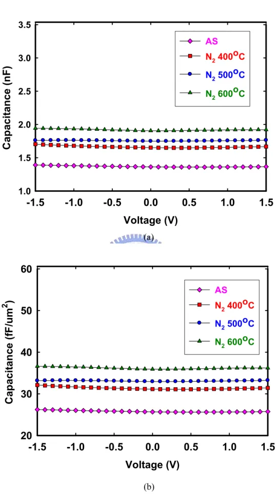
(54) mask. All these processes are performed at room temperature. Figure 3-2 shows the flow chart of HfO2 thin film fabrication with plasma process. The physical gate oxide thickness was determined by n&k analyzer 1280. The equivalent oxide thickness (EOT) was extracted by fitting the measured high-frequency capacitance-voltage (C-V) data from Hewlett-Packard (HP) 4284LCR meter under zero-biased. Moreover the capacitance was measure using 4284LCR meter at frequencies 100 KHz. In order investigate the thermal stability of high-k dielectric film. The tunneling leakage current density-voltage (J-V) was measured by semiconductor parameter analyzer HP4145A. After PDA temperature, the micro-roughness of the HfO2 surface was detected by atomic force microscopy (AFM).. 3.3 Results and Discussions. 3.3.1 Basic characteristic of the MIM with PDA Technology. After PDA process in N2, Figure 3-3 (a) C-V characteristics of MIM structure (Ta/HfO2/Ta) shows difference effects for electric characteristic at 100 KHz. The capacitance densities increase with PDA temperature. It may be due to the PDA processing in N2 ambient provides a reducing interface for oxidized surface layer of the Ta electrode [38]. Figure 3-3 (b) shows the capacitance densities was the highest value at PDA 600°C. The capacitance densities increase with PDA temperature be explained to Grain Boundary Barrier Layer Capacitor structure [39-41]. Effective permittivity of capacitor is related to the ratio of the average thicknesses of grain and. 39.
(55) grain boundary. Generally, the ratio of the average thicknesses of grain and grain boundary is very lager, so that the effective permittivity of capacitor is very high. Figure 3-4 shows J-V curves characteristics of MIM structure (Ta/HfO2/Ta) without PDA and with 400°C, 500°C, 600°C PDA in N2. Leakage current increases over 500°C PDA. It may be to grant growths in the high-k material. The corresponding AFM were presented in Figure 3-5 (a) and (b). Surface roughness of HfO2/Ta structure without PDA was 0.762nm. After PDA process, surface roughness increases from 0.803nm (400°C-60s), 1.115nm (500°C-60s) to 2.774nm (600°C-60s) in Figure 3-6, Figure 3-7, and Figure 3-8 [42]. At 600°C-60s PDA, surface roughness of the high-k material raises greatly. Due to stress relaxation and grain growth during annealing, the grain boundaries become clearly visible after PDA process [43]. For the as-deposited, 400°C, 500°C, and 600°C-annealed samples, higher annealing temperature lead to higher leakage current. Since the higher PDA temperature may trigger the small grains to merge into a large grain. The boundaries around these large grains will provide more short leakage path, which allow the carriers more easily tunneling through from top electrode to bottom electrode and, then, contribute to larger leakage current. Therefore, the crystalline temperature of HfO2 material was presented in our results. It is found that agglomeration effect might lead to higher gate leakage current density [42] and this is consistent with high leakage current in MIM structure we discussed before. Figure 3-9 shows the relationship between surfaces roughness relate to difference PDA temperature of HfO2/Ta structure, these results were understood clearly for grain growing and crystallizing at temperature. On the contrary, the capacitance of HfO2 samples annealing in an O2 ambient decreases with the increasing annealing temperature in Figure 3-10(a) and (b) [44]. Therefore, the capacitance decreases after annealing in an O2 ambient. This is because an O2 penetration will induce the increasing of the interfacial layer at HfO2/Ta and 40.
(56) higher annealing temperature increasing will speed up interface layer growth rate [45]. Figure 3-11 shows the J-V curves characteristics of MIM structure (Ta/HfO2/Ta) without PDA and with 400°C, 500°C, 600°C PDA in an O2 ambient. The current density reduces with PDA temperature, it may be to explain that thicker film of HfO2 was produced or oxygen vacancy within high-k material was decreased. Figure 3-12 the relationship between capacitance densities relate to difference PDA temperature. The comparison of difference PDA temperature in O2 or N2 ambient shows the capacitance densities rise after PDA process in N2 ambient. In the addition, the contrary results were produced after PDA process in O2 ambient. Figure 3-13 shows the leakage current of sample with 400°C PDA was lower than other PDA temperature in N2 ambient. It can be explained to the defects decrease after 400°C annealing in N2 ambient. As mentioned above, PDA process in O2 ambient can cause the leakage current to diminish.. 3.3.2 Basic characteristic of the MIM with Plasma surface Technology. Figure 3-14 (a), (b) shows C-V and J-V characteristics of MIM structure (Ta/HfO2/Ta) without PDA and with N2O, NH3 plasma process on Ta electrode. After plasma process, maybe the capacitance densities both were decreased due to interface layer growing. This interface layer was not understood for us. We need more physical analysis, for example TEM analysis, XRD analysis, and Auger depth profiles analysis. Leakage current density decreases after plasma processing, which is supposed to be suppressed by thicker interfacial layer on bottom metal. Figure 3-15, Figure 3-16, and Figure 3-17 clarify AFM topography of Ta bottom electrode without plasma process and with N2O, NH3 plasma process. Surface roughness without plasma process was 41.
(57) more than surface roughness with N2O, NH3 plasma process. It may be reason to decrease leakage current density. Figure 3-18 the comparison between surfaces roughness relate to without and with plasma process on Ta electrode. The results of N2O, NH3 plasma process on Ta metal clarify reduce leakage current, but capacitance density degrades.. 3.3.3 Analysis Voltage coefficient of capacitance (VCC) on the MIM. Voltage coefficient of capacitance (VCC) are very important parameters for MIM capacitor applications, and can be obtained by using a second order polynomial equation of. dC C (V ) − Co = = αV 2 + βV + 1 , C0 where is the zero-biased Co Co. capacitance, αand β represent the quadratic and linear VCC respectively. The requirement of the quadratic coefficient of capacitance α is smaller than 100 ppm/V2, and the requirement of the linear coefficient of capacitance β is below 1000 ppm/V according to the ITRS roadmap. Low VCC values cause the capacitance to stability. Figure 3-19, Figure 3-20, and Figure 3-21 shows Normalized C-V curves (△C/Co) of MIM structure (Ta/HfO2/Ta) relate to without PDA and with 400°C、500°C PDA in N2 for 100 KHz, 10 KHz, and 1KHz respectively. We found the sample exhibits VCC values became lager with increasing PDA temperature. Especially the sample with 500°C PDA in N2 clarifies high VCC values. It may be explained that the dielectric traps located around the metal–insulator interface [46]. Figure 3-22, Figure 3-23, and Figure 3-24 shows Normalized C-V curves (△C/Co) of MIM structure (Ta/HfO2/Ta) relate to without PDA and with 400°C、500°C PDA in O2 ambient for 100 KHz, 10. 42.
(58) KHz, and 1KHz respectively. The sample with 500°C PDA in O2 ambient can reduce VCC values compare with the sample with 400°C PDA in O2 ambient. It may be explained that PDA process with 500°C O2 ambient reduces traps around the metal–insulator interface. Figure 3-25 shows measured Quadratic VCC, α, versus difference frequency without PDA , with 400°C、500°C PDA in O2 and N2. It is found that the Quadratic VCC decreases with frequency. It may be explained that the carrier mobility becomes smaller with increase frequency, which lead to a higher relaxation time and a smaller capacitance variation [47]. Table 3-1 Summary of Quadratic VCC, α and linear VCC, β extracted from MIM structure (Ta/HfO2/Ta) without and with 400°C、500°C PDA in N2 and O2 ambient PDA process. Maybe dielectric traps located around the metal–insulator interface cause high VCC values. According to this reason, we use plasma process to improve metal–insulator interface defects [48]. Besides, the rapid △C/Co reduction with increasing frequency may be due to the trapped carriers being unable to follow the high frequency signal [49] [50]. Figure 3-26, Figure 3-27, Figure 3-28 shows Normalized C-V curves (△C/Co) of MIM structure (Ta/HfO2/Ta) relate to without plasma and with N2O, NH3 plasma process for 100 KHz, 10 KHz, and 1KHz respectively. We found VCC values of the sample with plasma process become smaller than the sample without plasma process. It may be explained that plasma process can improve trap defects to reduce VCC values. Figure 3-29 shows measured Quadratic VCC, α, versus difference frequency without plasma and with N2O, NH3 plasma process. The results clarify plasma process can reduce VCC values make the capacitance stability. However the VCC values are still higher than 100 ppm/V2 and 1000 ppm/V, not achieve the requirement of the ITRS roadmap. Table 3-2 Summary of Quadratic VCC, α, and linear VCC, β, extracted from MIM structure (Ta/HfO2/Ta) without plasma and with N2O, NH3 plasma process for variant frequency. 43.
(59) 3.4 Summary In this chapter, we studied PDA effect on MIM structure at first. We met a few questions of large leakage current density under high temperature annealing in N2 ambient. Because of grain growing, we found surface roughness increase with PDA temperature. High Surface roughness gives rise to large leakage current density. Moreover, PDA temperature increases to cause the capacitance go up, it was attributed grain boundary effect. On condition PDA in O2 ambient, after annealing O2 ambient the leakage current density reduces and capacitance rises were attributed thicker high-k film producing and interface layer growing. Secondly, we used plasma process improve electric characteristics on MIM. It was found that leakage current density decreases one order, but ensues to reduce capacitance density after plasma process. Especially N2O plasma process reduces capacitance density more than NH3 plasma process. It may be explained that surface roughness with N2O plasma process was higher than NH3 plasma process. Finally, form analysis VCC on MIM, we found out that PDA process in N2 ambient causes Quadratic VCC and linear VCC become higher than without PDA and with PDA process in O2 ambient. Especially Quadratic VCC and linear VCC become smaller after 500°C PDA process in O2 ambient. Besides, plasma process can reduce Quadratic VCC, but still not achieve the requirement of the ITRS roadmap.. 44.
(60) 1. Silicon substrate, RCA clean and HF dip to remove native oxide.. 2. SiO2 550 nm film deposited at furnace Wet Oxidation.. 3. Bottom electrode Tantalum 100 nm deposited by Reactive Sputter (RS) and is patterned by mask. 4. The HfO2 thin film 5 nm deposited by RS. 5. Post deposit annealing, PDA: 400°C, 500°C, 600°C, in N2 or O2 60 sec.. 6. Finally, Top Electrode deposited 100 nm by RS and is patterned by metal mask. Figure 3-1 Flow chart for the fabrication of HfO2 thin films with PDA Technology. 45.
(61) 1. Silicon substrate, RCA clean and HF dip to remove native oxide.. 2. SiO2 550 nm film deposited at furnace Wet Oxidation.. 3. Bottom electrode Tantalum 100 nm deposited by Reactive Sputter (RS) and is patterned by mask. 4. Plasma N2O and NH3 treatment on Bottom electrode. 5. The HfO2 thin film 5 nm deposited by RS. 6. Finally, Top Electrode deposited 100 nm by RS and is patterned by metal mask. Figure 3-2 Flow chart for the fabrication of HfO2 thin films with Plasma Technology. 46.
(62) 3.5 AS N2 400oC. Capacitance (nF). 3.0. N2 500oC N2 600oC. 2.5. 2.0. 1.5. 1.0. -1.5. -1.0. -0.5. 0.0. 0.5. 1.0. 1.5. Voltage (V) (a). 60 Capacitance (fF/um2). AS N2 400oC. 50. N2 500oC N2 600oC. 40. 30. 20 -1.5. -1.0. -0.5. 0.0. 0.5. 1.0. 1.5. Voltage (V) (b) Figure 3-3 The comparison of (a) and (b) C-V characteristics of MIM structure (Ta/HfO2/Ta) without PDA and with 400°C, 500°C , 600°C PDA in N2. 47.
(63) 2. J (A/cm ). 101 100. AS. 10-1. N2 400oC. 10-2. N2 500oC. 10-3. N2 600oC. 10-4 10-5 10-6 10-7 10-8 10-9 -1.5. -1.0. -0.5. 0.0. 0.5. 1.0. 1.5. Voltae (V) Figure 3-4 The J-V curves characteristics of MIM structure (Ta/HfO2/Ta) without PDA and with 400°C, 500°C, 600°C PDA in N2. 48.
(64) (a). (b) Figure 3-5 (a) and (b) AFM topography of HfO2/Ta structure without PDA. 49.
(65) (a). (b) Figure 3-6 (a) and (b) AFM topography of HfO2/Ta structure with 400°C PDA in N2 50.
(66) (a). (b) Figure 3-7 (a) and (b) AFM topography of HfO2/Ta structure with 500°C PDA in N2. 51.
(67) (a). (b) Figure 3-8 (a) and (b) AFM topography of HfO2/Ta structure with 600°C PDA in N2 52.
(68) 30. RMS (A). 25 20 15 10 5. AS-dep.. 400. 500. 600. Figure 3-9 the relationship between surfaces roughness relate to difference PDA temperature of HfO2/Ta structure. 53.
(69) 1.8 1.6 Capacitance (nF). 1.4 1.2 1.0 AS. 0.8. O2 400oC. 0.6. O2 500oC. 0.4. O. O2 600 C. 0.2 0.0 -1.5. -1.0. -0.5. 0.0. 0.5. 1.0. 1.5. Voltage (V) (a). 25. 2. Capacitance (fF/um ). 30. 20 15. AS. 10. O2 500oC. O2 400oC O2 600oC. 5 0 -1.5. -1.0. -0.5. 0.0. 0.5. 1.0. 1.5. Voltage (V) (b) Figure 3-10 (a) and (b) C-V characteristics of MIM structure (Ta/HfO2/Ta) without PDA and with 400°C, 500°C, 600°C PDA in O2 54.
(70) 2. J (A/cm ). 100 10-1 10-2 10-3 10-4 10-5 10-6 10-7 10-8 10-9 10-10 10-11 10-12 -1.5. AS o O2 400 C O2 500oC O2 600oC. -1.0. -0.5. 0.0. 0.5. 1.0. 1.5. Voltage (V) Figure 3-11 the J-V curves characteristics of MIM structure (Ta/HfO2/Ta) without PDA and with 400°C, 500°C, 600°C PDA in O2. 2. Capacitance (fF/um ). 50. 40. N2 O2 AS-dep.. 30. 20 AS-dep.. 400. 500. 600. PDA Temperature (oC) Figure 3-12 the relationship between capacitance densities relate to difference PDA temperature 55.
(71) 2. J (A/cm ) @ -1V. 10-1 10-2. N2. 10-3. O2 AS-dep.. 10-4 10-5 10-6 10-7 10-8 10-9 10-10 10-11. AS-dep.. 400. 500. 600. PDA Temperature (oC) Figure 3-13 leakage current characteristics as a function of PDA temperatures with 400°C, 500°C and 600°C deposition in N2 and O2.. 56.
(72) Capacitance (fF/um2). 30. 25. 20 AS N2O. 15. NH3. 10 -1.5. -1.0. -0.5. 0.0. 0.5. 1.0. 1.5. Voltage (V) (a). 10-2 10-3. AS Plasma NH3. 2. J (A/cm ). 10-4. Plasma N2O. 10-5 10-6 10-7 10-8 10-9 10-10 -1.5. -1.0. -0.5. 0.0. 0.5. 1.0. 1.5. Voltage (V) (b) Figure 3-14 the comparison of (a) C-V and (b) J-V characteristics of MIM structure (Ta/HfO2/Ta) without PDA and with N2O, NH3 plasma process on Ta electrode. 57.
(73) Figure 3-15 AFM topography of Ta bottom electrode without plasma process. 58.
(74) Figure 3-16 AFM topography of Ta bottom electrode with N2O plasma process, 600s. 59.
(75) Figure 3-17 AFM topography of Ta bottom electrode with NH3 plasma process, 600s. 60.
(76) 14. RMS (A). 12 10 8 6 AS-dep.. N2O Plasma. NH3 Plasma. Figure 3-18 the relationship between surfaces roughness relate to without and with plasma process on Ta electrode. 61.
(77) 50000. AS 0 N2 400 C. 40000. 0. dC/C0 (ppm). N2 500 C. 30000 20000 10000. 100KHz. 0 -1.5. -1.0. -0.5. 0.0. 0.5. 1.0. 1.5. Voltage (V) Figure 3-19 Normalized C-V curves (△C/Co) of MIM structure (Ta/HfO2/Ta) relate to without PDA and with 400°C、500°C PDA in N2 for 100 KHz. 50000. AS 0 N2 400 C. 40000. 0. dC/C0 (ppm). N2 500 C. 30000 20000 10000. 10KHz. 0 -1.5. -1.0. -0.5. 0.0. 0.5. 1.0. 1.5. Voltage (V) Figure 3-20 Normalized C-V curves (△C/Co) of MIM structure (Ta/HfO2/Ta) relate to without PDA and with 400°C、500°C PDA in N2 for 10 KHz 62.
(78) 160000 AS 0 N2 400 C. 140000. dC/C0 (ppm). 120000. 0. N2 500 C. 100000 80000 60000 40000 20000. 1KHz. 0 -1.5. -1.0. -0.5. 0.0. 0.5. 1.0. 1.5. Voltage (V) Figure 3-21 Normalized C-V curves (△C/Co) of MIM structure (Ta/HfO2/Ta) relate to without PDA and with 400°C、500°C PDA in N2 for 1 KHz. dC/C0 (ppm). 25000 20000. AS 0 O2 400 C. 15000. O2 500 C. 0. 10000 5000 0 -5000. 100KHz -1.5. -1.0. -0.5. 0.0. 0.5. 1.0. 1.5. Voltage (V) Figure 3-22 Normalized C-V curves (△C/Co) of MIM structure (Ta/HfO2/Ta) relate to without PDA and with 400°C、500°C PDA in O2 for 100 KHz 63.
(79) 35000 30000 25000. AS 0 O2 400 C. 20000. O2 500 C. dC/C0 (ppm). 0. 15000 10000 5000 0. 10KHz. -5000 -1.5. -1.0. -0.5. 0.0. 0.5. 1.0. 1.5. Voltage (V). Figure 3-23 Normalized C-V curves (△C/Co) of MIM structure (Ta/HfO2/Ta) relate to without PDA and with 400°C、500°C PDA in O2 for 10 KHz. dC/C0 (ppm). 60000 50000. AS 0 O2 400 C. 40000. O2 500 C. 0. 30000 20000 10000 0. 1KHz. -10000 -1.5. -1.0. -0.5. 0.0. 0.5. 1.0. 1.5. Voltage (V) Figure 3-24 Normalized C-V curves (△C/Co) of MIM structure (Ta/HfO2/Ta) relate to without PDA and with 400°C、500°C PDA in O2 for 1 KHz 64.
(80) 40000 35000. AS-dep. 0 O2 400 C. 2 α (ppm/V ). 30000. 0. O2 500 C. 25000. 0. N2 400 C 0. 20000. N2 500 C. 15000 10000 5000 0. 1K. 10K 100k Frequency (Hz). Figure 3-25 Quadratic VCC, α, versus difference frequency without PDA , with 400°C、500°C PDA in N2 and 400°C、500°C PDA in O2. 65.
(81) As-dep.. 400°C PDA in O2. 500°C PDA in O2. 400°C PDA in N2. 500°C PDA in N2. Frequency(Hz). α (ppm/V2). β (ppm/V). 1K. 14215. 17200. 10K. 8277. 10536. 100K. 5139. 7025. 1K. 12322. 6942. 10K. 8069. 7512. 100K. 3361. 1465. 1K. 7842. 2696. 10K. 4580. 2044. 100K. 2833. 1696. 1K. 21882. 15700. 10K. 11285. 9305. 100K. 9049. 7181. 1K. 35714. 31992. 10K. 16170. 13406. 100K. 10291. 9114. Table 3-1 Summary of Quadratic VCC, α and linear VCC, β extracted from MIM structure (Ta/HfO2/Ta) without and with 400°C、500°C in N2, 400°C、500°C in O2 PDA.. 66.
(82) 25000. AS N2O. 20000. dC/C0 (ppm). 15000. NH3. 10000 5000 0 -5000 -10000. 100k Hz -1.5. -1.0. -0.5. 0.0. 0.5. 1.0. 1.5. Voltage (V) Figure 3-26 Normalized C-V curves (△C/Co) of MIM structure (Ta/HfO2/Ta) relate to without plasma and with N2O, NH3 plasma process for 100 KHz. 35000. AS N 2O. 30000 25000 dC/C0 (ppm). 20000. NH3. 15000 10000 5000 0 -5000. 10K Hz. -10000 -15000. -1.5. -1.0. -0.5. 0.0. 0.5. 1.0. 1.5. Voltage (V) Figure 3-27 Normalized C-V curves (△C/Co) of MIM structure (Ta/HfO2/Ta) relate to 67.
數據
+7
相關文件
C.轄屬各樂齡學習中心 數超過 25 所者,103 年 度於平面媒體(含報 紙、雜誌)刊出達 12 則 以上,並結合廣播電
◦ 金屬介電層 (inter-metal dielectric, IMD) 是介於兩 個金屬層中間,就像兩個導電的金屬或是兩條鄰 近的金屬線之間的絕緣薄膜,並以階梯覆蓋 (step
Thus any continuous vector function r defines a space curve C that is traced out by the tip of the moving vector r(t), as shown in Figure 1.... The curve, shown in Figure 2,
The function f whose graph is shown in Figure 9 is defined on the closed interval [0, 2] but has no maximum value. The function takes on values arbitrarily close to 3, but
Then we can draw a right triangle with angle θ as in Figure 3 and deduce from the Pythagorean Theorem that the third side has length.. This enables us to read from the
But for double integrals, we want to be able to integrate a function f not just over rectangles but also over regions D of more general shape, such as the one illustrated in
Figure 6 shows the relationship between the increment ∆y and the differential dy: ∆y represents the change in height of the curve y = f(x) and dy represents the change in height
Figure 3: Comparison of the partitioning of the hemisphere effected by a VQPCA-based model (left) and a PPCA mixture model (right). The illustrated boundaries delineate regions of
![TraditionalMLCalgorithmsmainlytacklethebatchMLCproblem,wheretheinputdataarepresentedinabatch[24,28].Nevertheless,inmanyMLCapplicationssuchase-mailcategorization[22],multi-labelexamplesarriveasastream.Onlineanalysisistherefore dimensionreducermotivatedbyma](data:image/gif;base64,R0lGODlhAQABAIAAAP///wAAACH5BAEAAAAALAAAAAABAAEAAAICRAEAOw==)