Deep-level emissions in Ga As N Ga As structures grown by metal organic chemical
vapor deposition
J. F. Chen, C. T. Ke, P. C. Hsieh, C. H. Chiang, W. I. Lee, and S. C. Lee
Citation: Journal of Applied Physics 101, 123515 (2007); doi: 10.1063/1.2748613
View online: http://dx.doi.org/10.1063/1.2748613
View Table of Contents: http://scitation.aip.org/content/aip/journal/jap/101/12?ver=pdfcov Published by the AIP Publishing
Articles you may be interested in
Contactless electroreflectance of Ga In N As Sb Ga As single quantum wells with indium content of 8%–32% J. Appl. Phys. 101, 013504 (2007); 10.1063/1.2382721
Thermal quenching mechanism of photoluminescence in 1.55 m Ga In N As Sb Ga ( N ) As quantum-well structures
Appl. Phys. Lett. 89, 101909 (2006); 10.1063/1.2345240
Nonlinear optical transitions of Ga As Al Ga As asymmetric double-well structures Appl. Phys. Lett. 89, 032114 (2006); 10.1063/1.2220533
Carrier relaxation dynamics in annealed and hydrogenated ( Ga In ) ( N As ) Ga As quantum wells Appl. Phys. Lett. 87, 252111 (2005); 10.1063/1.2149154
Photoreflectance and photoluminescence investigations of a step-like Ga In N As Sb Ga As N Ga As quantum well tailored at 1.5 m : The energy level structure and the Stokes shift
J. Appl. Phys. 97, 053515 (2005); 10.1063/1.1854729
Deep-level emissions in GaAsN / GaAs structures grown
by metal organic chemical vapor deposition
J. F. Chen,a兲C. T. Ke, P. C. Hsieh, C. H. Chiang, W. I. Lee, and S. C. Lee
Department of Electrophysics, National Chiao Tung University, Hsinchu, 30059m Taiwan 30010, Republic of China
共Received 26 December 2006; accepted 6 May 2007; published online 22 June 2007兲
This work presents the deep-level photoluminescence of coherently strained GaAsN / GaAs quantum-well共QW兲 structures with various GaAsN thicknesses and N contents. A broad deep-level emission at⬃1.1 eV is observed, whose wavelength is redshifted as the GaAsN thickness increases. Based on its energy separation from the QW emission, this emission is attributed to a transition between the QW electron ground state and a deep level at⬃0.2 eV above the GaAsN valence-band 共VB兲 edge. This level is shown to be tied to the GaAs band edge. A transition between this level and the GaAs conduction band allows the GaAsN–GaAs band alignment to be evaluated. A type II band lineup is obtained with VB offsets of 0.03 and 0.002 eV for N = 0.6% and 1.8%, respectively. The decreased VB offset suggests a transition from type II to type I with increasing N content. Thermal annealing effectively removes this level and improves the QW emission. The concentration of this level is not clearly correlated with N content, suggesting that this level is induced by a low-temperature growth of the GaAsN layer to suppress the composition fluctuation. Given its energy, this level is tentatively assigned to VGa. © 2007 American Institute of Physics.
关DOI:10.1063/1.2748613兴
I. INTRODUCTION
The large differences between both sizes and atomic or-bital energies of the As and N atoms cause the GaAsN band gap to decrease considerably as the N content increases.1–10 The optical bowing coefficient is very large and depends strongly on composition.3–7 Wei and Zunger6 have divided the GaAsN band gap into two regions:共i兲 a bandlike region in which the bowing coefficient is relatively small and共ii兲 an impuritylike region 共dilute N兲 in which the bowing coeffi-cient is larger and composition dependent. A controversy re-mains over whether the band alignment for dilute N is type I10–12or type II.5,8,9Experimental evaluation of the valence-band 共VB兲 alignment is difficult because the experimental uncertainty often exceeds the very small VB offset.8–12Deep levels with their strongly localized wave functions can be used as probes of interfacial band structures.13,14 However, the properties of the deep levels and their related emissions in this material system have seldom been reported.
This work investigates the deep-level emissions of the GaAsN / GaAs single-quantum-well 共SQW兲 structures with various GaAsN thicknesses and N compositions. A promi-nent deep-level emission at ⬃1.1 eV which exhibits a quantum-size-confinement effect is presented here. The ef-fects of temperature, excitation power, and postgrowth an-nealing on this emission are studied. Transitions that involve this level are analyzed to evaluate the GaAsN / GaAs band alignment. Moreover, the assignment of the 1.1 eV emission is discussed.
II. EXPERIMENTS
The GaAs/ GaAsN / GaAs SQW samples were grown on
n+-GaAs 共001兲 substrates by low-pressure metal organic
chemical vapor deposition共MOCVD兲. The GaAsN layer was undoped to avoid the introduction of any unwanted shallow impurity states. This GaAsN layer was inserted between two 0.3m Si-doped GaAs layers with a concentration of 6 ⫻1016cm−3for electrical measurements. The GaAsN layers
were grown at⬃500 °C using dimethylhydrazine 共DMHY兲 as a nitrogen source in combination with triethylgallium and AsH3. Detailed growth conditions can be found elsewhere.15
The N content was determined from double-crystal x-ray dif-fraction and verified with photoluminescence 共PL兲 peak en-ergy. None of the studied samples showed strain relaxation, according to their x-ray diffraction patterns which show clear interference fringes.15 PL spectra were measured using an excitation of the 532 nm line from a solid-state laser.
III. MEASUREMENTS AND RESULTS
A. Thickness-dependence of the PL spectra
Figure 1 shows the 30 K PL spectra of the N = 1.8% SQW samples with GaAsN thickness ranging from 40 to 250 Å. Each spectrum generally consists of two peaks. The high-energy peak originates from the GaAsN quantum states, as evidenced by the redshift of the emission energy with the increase in the GaAsN thickness. The line shape is quite symmetric without the previously reported low-energy tail,16 suggesting no obvious compositional fluctuation. Lower growth temperatures of the GaAsN layer may sup-press the compositional fluctuation but degrade optical prop-erties due to the formation of recombination centers. In ad-dition to the QW emission, a broad peak arises at the
low-a兲Electronic mail: [email protected]
0021-8979/2007/101共12兲/123515/4/$23.00 101, 123515-1 © 2007 American Institute of Physics
energy side. This peak is considered to originate from a deep level and is designated as “1.1 eV emission” because of the proximity of peak emission energies. Similar defect emis-sions have been reported9,17,18 but no detailed properties. This deep-level emission displays a similar size-confinement effect as QW emission. The wavelength of the deep-level emission shifts from 1.159 to 1.028 eV as the GaAsN thick-ness increases from 40 to 250 Å. Notably, the energy sepa-ration between this and the QW emissions remains a constant ⬃0.2 eV.
Since a spatially indirect transition normally has a very small transition probability, the prominence of the 1.1 eV emission and its size-confinement effect indicate a strong spatial correlation between the corresponding deep level and the GaAsN well. Thus, the authors believe that the deep level is in or around the GaAsN well rather than in the GaAs substrate which is at least ⬃0.3m from the GaAsN well. Since the wave function for an electron that is trapped on a deep defect state is strongly localized, further confinement due to the well width is expected to be very weak. Thus, a reasonable explanation for the size-confinement effect is that the 1.1 eV emission must involve the ground state of the GaAsN well. Although controversy remains over whether the alignment is type I or II, the band gap bowing in GaAsN / GaAs共dilute N兲 is commonly accepted to be mainly in the conduction band共CB兲 with a very small VB offset.8–12 Thus, the 1.1 eV emission is regarded as a transition between the QW electron ground state共EGS兲 and the deep level. The energy difference between the 1.1 eV and QW emissions is
the energy location of this deep level relative to the GaAsN VB edge, which is at ⬃0.2 eV above the GaAsN VB edge. The 1.1 eV emission cannot be an indirect transition in real space between the QW EGS and the neighboring GaAs VB because if it were, the VB offset would be 0.2 eV which is too large.
B. Power and temperature dependence of the 1.1 eV emission
Figure2shows the power and temperature dependences of the PL spectra of the 60 Å GaAsN sample with N = 1.8% to elucidate the recombination mechanism of the deep-level emission. At low excitation power 共1.3 and 3.3 mW兲, the QW emission is weak and the spectrum is dominated by the deep-level emission, as shown in Fig.2共a兲. As the excitation power increases, the deep-level emission gradually becomes saturated and, at 6.5 mW, is dominated by the QW emission. This finding indicates that the photo-generated carriers initially occupy the deep level because it is at a lower energy than the QW emission. When the power excitation is raised, further photogenerated carriers must oc-cupy the higher QW state because the concentration of the deep level is limited. The line shape of the 1.1 eV emission is rather symmetrical as the QW emission, consistent with the fact that both emissions involve the same QW EGS. The temperature dependence in Fig.2共b兲shows that the intensi-ties of both the QW and the 1.1 eV emissions decrease as temperature is increased. The QW peak displays a clear red-shift with increasing temperature, whereas no red-shift in the 1.1 eV emission is evident because of linewidth broadening. FIG. 1. 30 K PL spectra of the N = 1.8% GaAsN / GaAs SQW samples with
different GaAsN thicknesses at an excitation power of 6.5 mW. Besides the QW emission, each spectrum displays at the lower energy side a broad emission at⬃1.1 eV, which is shifted along with the QW emission. The energy separation between this and the QW emissions is about 0.2 eV, sug-gesting that the 1.1 eV emission is a transition that involves the electron ground state in the well and a deep level state at about 0.2 eV above the GaAsN valence-band edge.
FIG. 2.共a兲 Power and 共b兲 temperature dependences of the PL spectra of the 60 Å GaAsN sample with N = 1.8%. At low excitation power, the 1.1 eV deep-level emission dominates the QW emission; however, at high excita-tion power, the QW emission dominates the deep-level emission.
123515-2 Chen et al. J. Appl. Phys. 101, 123515共2007兲
The data are not sufficiently detailed to draw any conclusions on the thermal effect of wave-function localization of the deep level.
C. Composition dependence of the deep-level emissions
Figure1shows an additional weak peak at 1.318 eV in the 250 Å sample. This peak is not clearly seen in the other samples probably because of its proximity to the QW peak. Figure3 shows the composition dependence of this peak in the 30 K PL spectra of the 250 Å GaAsN samples with N = 0.6% and 1.8%, as indicated by the vertical dashed line. For a GaAsN thickness of 250 Å, the QW confinement effect is negligible and the QW emission energy can be regarded as the GaAsN band gap, regardless of whether the band lineup is type I or II. Increasing the N content shifts the QW emis-sion from 1.387 to 1.214 eV and the deep-level emisemis-sion from 1.180 to 1.025 eV. As discussed above, the energy separation between these two emissions is the deep level position above the GaAsN VB edge, which is 0.207 and 0.189 eV for N = 0.6% and 1.8%, respectively, as shown in the schematic band diagrams in Fig. 4, in which the deep level is shown by a dashed line. For an assumed zero VB offset and a GaAs band gap of 1.505 eV, the defect level would be at 1.298 and 1.316 eV below the GaAs CB edge for N = 0.6% and 1.8%, respectively. Notably, these levels are comparable to the additional weak emissions at 1.328 and 1.318 eV observed in Fig.3for N = 0.6% and 1.8%, respec-tively. Therefore, these emissions are assigned to transitions between the GaAs CB edge and the deep level, and the dif-ferences of 0.03 and 0.002 eV are attributed to the VB off-sets. This result shows that the band alignment is type II with a very small VB offset. Sakai et al.5theoretically predicted the type II alignment, and Kitatani et al.8used x-ray photo-electron spectroscopy共XPS兲 to support this prediction. Sun
et al.9 also reported a type II alignment with a VB offset of 0.04 eV for N = 1.5%, which is close to the value of 0.028 eV that was obtained by XPS.8 However, the very
small VB offset 共0.002 eV兲 for N=1.8% suggests the possi-bility of a transition to type I as the N content increases. This possibility may explain the type I alignment that was also predicted by first-principle calculations10 and supported by PL11and hole-confinement measurements.12N content must be further increased to verify this claim.
The energy perturbation of the deep level that is caused by the band discontinuity across the interface must also be considered. The strong localization of the wave function for a carrier trapped on a deep defect state19 causes the energy perturbation of the deep level to be significant only within a few angstroms around the interface. In the GaAs/ GaAsN system in which the VB offset is very small, a negligible energy perturbation of the deep level can be expected. Thus, the deep level is shown as continuous across the interface, as illustrated in Fig. 4. This result suggests the possibility of using this deep level as a common reference13 for probing the interfacial band structure of a heterostructure.
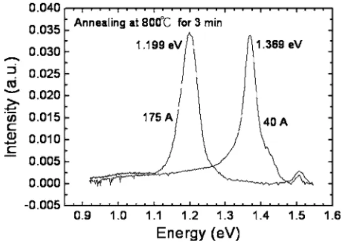
D. Effect of annealing on deep-level emissions
As shown in Fig. 4, the CB offset increases from 0.148 to 0.293 eV as the N content increases from 0.6% to 1.8%, suggesting a downward shift of 0.145 eV in the GaAsN CB edge. This downward shift does not move the deep level downward. Instead, the deep level is shifted up-ward by 0.01 eV. If this small upup-ward shift is neglected, then the deep level is tied to the GaAs band edge. This is a char-acteristic of a GaAs point defect rather than a N-related de-fect. This defect can be effectively removed by postgrowth annealing. Figure5shows the 30 K PL spectra of the 40 and 175 Å samples 共N=1.8%兲 after annealing at 800 °C for 3 min. A comparison with the spectra of the as-grown samples in Fig.1reveals that annealing produces no signifi-FIG. 3. 30 K PL spectra of the 250 Å GaAsN samples with N = 0.6% and
1.8%. Besides the QW and the 1.1 eV emissions, each spectrum shows an additional peak at 1.328共1.318兲 eV for N=0.6% 共1.8%兲, which is attributed to a transition between the deep level and the GaAs CB.
FIG. 4. Schematic energy band diagrams for 250 Å GaAsN samples with N = 0.6% and 1.8%, respectively. The diagrams illustrate the deep levels and their experimentally observed transitions.
cant energy shift of the QW emission, suggesting no appar-ent interdiffusion. This is consistappar-ent with the secondary ion mass spectroscopy 共SIMS兲 result that shows no significant drop of the N concentration in the QW region after anneal-ing. In both samples, annealing increases the intensity of the QW emission. This improved efficiency can be attributed to the removal of deep levels. Notably, the 1.1 eV emission becomes nearly invisible after annealing, suggesting that an-nealing can remove the corresponding deep level. This find-ing is consistent with the assignment of a GaAs point defect for the 1.1 eV emission rather than N-related impurities.
Another reason to exclude N-related defects, such as N interstitials, for the 1.1 eV emission is that if they were in-volved, the intensity of the 1.1 eV emission would increase with the N content from 0.6% to 1.8%. However, the experi-mental data in Fig. 3 show no such trend. Thus, the deep level originates from a GaAs point defect. This level is at 0.177 共0.187兲 eV above the GaAs VB edge for N=0.6% 共1.8%兲. In view of this energy position, we speculate that the deep level is associated with gallium vacancies VGa which were reported to be at ⬃0.2 eV above the GaAs VB edge and was a radiative defect.20–22 The transition between this defect and GaAs CB would emit at ⬃1.25 eV which was commonly observed in liquid encapsulated Czochralski 共LEC兲 GaAs substrates.20
Chiang and Pearson21and Ohbu et
al.22 observed a similar emission at ⬃1.255 eV in GaAs films grown at low temperature and assigned it to VGa. This
defect is very close to the 1.1 eV deep level. In view of the energy proximity, the deep level is assigned tentatively to
VGa. This level may be the hole trap at 0.23 eV previously
observed in p-type In0.07Ga0.93As0.98N0.02 on GaAs by
deep-level transient spectroscopy 共DLTS兲.23 The presence of VGa
is supported by the previous observation of EL6 共Asi or
Asi-VGa complex兲 and EL2 共AsGa兲 traps by DLTS in
GaAsN / GaAs samples.15,24 If Asi is available, the presence
of VGa would favor the formation of AsGa according to the
reaction:25 Asi+ VGa→AsGa. Low-temperature grown GaAs
is known to contain a high concentration of point defects such as AsGaand VGa;26therefore, the presence of VGain the
GaAsN layer is reasonably suggested to be due to the low-temperature growth of the GaAsN layer to enhance the
in-corporation of N and suppress the compositional fluctuation. The results hereinto show that the VGa-related deep level is
radiative and is tied to the GaAs band edge. Therefore, pur-posely introducing this level enables the GaAsN / GaAs band offset to be evaluated by analyzing its related transitions.
IV. CONCLUSIONS
Deep-level emissions of GaAsN / GaAs SQW structures were investigated. PL spectra show prominent emission at ⬃1.1 eV, which exhibits a similarly sized confinement effect as the QW emission. This emission is attributed to a transi-tion between the QW electron ground state and a deep level. This deep level is tied to the GaAs band edge and, because of its energy position, is tentatively assigned to VGa.
Further-more, the PL spectra display an additional emission, which is attributed to a transition between the deep level and the GaAs conduction band. Using this deep level as a common reference, the GaAsN – GaAs band alignment is evaluated to be type II with valence-band offsets of 0.03 and 0.002 eV for N = 0.6% and 1.8%, respectively.
ACKNOWLEDGMENTS
The authors would like to thank the National Science Council of Taiwan, Republic of China for financially sup-porting this research under Contract No. NSC-95-2112-M-009-010 and the MOE, ATU programs.
1M. Kondow, S. Nakatsuka, T. Kitatani, Y. Yazawa, and M. Okai, Electron.
Lett. 32, 2244共1996兲.
2S. Sato, Y. Osawa, and T. Saitoh, Jpn. J. Appl. Phys., Part 1 36, 2671
共1997兲.
3L. Bellaiche and A. Zunger, Phys. Rev. B 57, 4425共1998兲.
4S. R. Kurtz, A. A. Alleman, E. D. Jones, J. M. Gee, J. J. Banas, and B. E.
Hammons, Appl. Phys. Lett. 74, 729共1999兲.
5S. Sakai, Y. Ueta, and Y. Teauchi, Jpn. J. Appl. Phys., Part 1 32, 4413
共1993兲.
6S. H. Wei and A. Zunger, Phys. Rev. Lett. 76, 664共1996兲. 7W. G. Bi and C. W. Tu, Appl. Phys. Lett. 70, 1608共1997兲.
8T. Kitatani, M. Kondow, T. Kikawa, Y. Yazawa, M. Okai, and K. Uomi,
Jpn. J. Appl. Phys., Part 1 38, 5003共1999兲.
9B. Q. Sun, D. S. Jiang, X. D. Luo, Z. Y. Xu, Z. Pan, L. H. Li, and R. H.
Wu, Appl. Phys. Lett. 76, 2862共2000兲.
10L. Bellaiche, S.-H. Wei, and A. Zunger, Phys. Rev. B 56, 10233共1997兲. 11I. A. Buyanova, G. Pozina, P. N. Hai, W. M. Chen, H. P. Xin, and C. W.
Tu, Phys. Rev. B 63, 033303共2000兲.
12P. Krispin, S. G. Spruytte, J. S. Harris, and K. H. Ploog, J. Appl. Phys. 88,
4153共2000兲.
13J. M. Langer and H. Heinrich, Phys. Rev. Lett. 55, 1414共1985兲. 14P. Krispin, J.-L. Lazzari, and H. Kostial, J. Appl. Phys. 84, 6135共1998兲. 15J. F. Chen, R. S. Hsiao, M. T. Hsieh, W. D. Huang, P. S. Guo, W. I. Lee,
S. C. Lee, and C. L. Lee, Jpn. J. Appl. Phys., Part 1 44, 7505共2005兲.
16I. A. Buyanova, W. M. Chen, G. Pozina, J. P. Bergman, H. P. Xin, and C.
W. Tu, Appl. Phys. Lett. 75, 501共1999兲.
17M. Weyers and M. Sato, Appl. Phys. Lett. 62, 1396共1993兲.
18M. Weyers, M. Sato, and H. Ando, Jpn. J. Appl. Phys., Part 2 31, L853
共1992兲.
19D. Stievenard and S. L. Feng, Mater. Sci. Forum 38, 679共1989兲. 20P. W. Yu, G. D. Robinson, J. R. Sizelove, and C. E. Stutz, Phys. Rev. B 49,
4689共1994兲.
21S. Y. Chiang and G. E. Pearson, J. Lumin. 10, 313共1975兲.
22I. Ohbu, M. Takahama, and K. Hiruma, Appl. Phys. Lett. 61, 1679共1992兲. 23D. Kwon, R. J. Kaplar, S. A. Ringel, A. A. Allerma, S. R. Kurtz, and E. D.
Jones, Appl. Phys. Lett. 74, 2830共1999兲.
24A. Y. Polyakov et al., Solid-State Electron. 46, 2141共2002兲. 25A. C. Irvine and D. W. Palmer, Phys. Rev. Lett. 68, 2168共1992兲. 26D. C. Look, Thin Solid Films 231, 61共1993兲.
FIG. 5. Effect of annealing at 800 ° C for 3 min on the 30 K PL spectra of the 40 and 175 Å GaAsN samples with N = 1.8%. The deep-level emissions seen in Fig.1are nearly absent.
123515-4 Chen et al. J. Appl. Phys. 101, 123515共2007兲