Mechanical Properties of Intermetallic Compounds on
Lead-Free Solder by Moire´ Techniques
ITING TSAI,1ENBOA WU,2 S.F. YEN,3and T.H. CHUANG3
1.—Institute of Applied Mechanics, National Taiwan University, Taiwan, R.O.C. 2.—Hong Kong Applied Science and Technology Research Institute Company Limited; email [email protected]. 3.—Department of Materials Science and Engineering, National Taiwan University, Taiwan, R.O.C. In this paper, methods for determining elastic moduli and coefficients of thermal expansion (CTE) of intermetallic compounds (IMC) formed at the interfaces between lead-free solder and metal substrates are presented. For the determination of elastic moduli, two kinds of lead-free solder—SnZn and Sn—were used; the metal substrates were copper and nickel. Nanoindentation techniques were adopted to determine the elastic moduli of Cu33.5Zn66.6, Cu3Sn, Cu6Sn5, and Ni3Sn4. Results for Cu33.5Zn66.6are new to the literature, and others values are in good agreement with those presented in the litera-ture. On the other hand, for CTE determination, two moire´ techniques, namely reflection moire´ and shadow moire´, were developed to measure the deformation of IMC/metal composite structures subjected to thermal loading. Finite-element analyses using ANSYS were then performed as a convolutional process, and the genetic search algorithm was used to optimally obtain the CTE of IMC. The CTE of Cu33.5Zn66.6was found to be approximate to that of copper, and the CTE of Cu3Sn was 10% larger. This method is also applicable to on-wafer films and IMC on micrometer order, such as the case of solder/ IMC/under bump metallization.
Key words: Intermetallic compound (IMC), lead-free, coefficients of thermal expansion (CTE)
INTRODUCTION
Intermetallic compounds (IMCs) are formed when interconnections in integrated circuit (IC) packages are jointed with solder. Although IMCs are not present in large amounts, they usually have a dom-inant influence on the reliability of the interconnec-tions because of their characteristic material properties. The effect is even more severe when the IMC forms a continuous layer between the interface of solder and the thin metal layer of joints. Individual mechanical properties of a solder/IMC/ under bump metallization (UBM) layered structure are required for simulation and analyses of the interconnection reliability, but they are always dif-ficult to determine because the thickness of each layer is on the order of micrometers. Furthermore, it is often impossible to separate each thin layer for testing with commercially available testing machines. Therefore, little has been reported con-cerning both elastic moduli and coefficients of
ther-mal expansion (CTE) of IMCs formed from soldering reactions to date.
Nanoindentation techniques have been applied to investigate the properties of microscale materials for years. Their extended capabilities are still under exploration, and applications to IMC material prop-erties have emerged only recently.1–4In this paper, nanoindentation techniques were adopted to deter-mine the elastic moduli of four different IMCs.
High-accuracy optical measurement techniques have been widely developed in various areas owing to their noncontact and whole-field properties. To quantify the interfering fringe patterns and to improve the resolution, stepping, phase-unwrapping, and image-processing techniques were required and developed.5–7 Asundi used the com-puter generated logical moire´ in both static and dynamic applications.6Chiang measured the stress in thin films by rotating the grating 90° to form slope fringe patterns in the other orthogonal direc-tion.8 However, rotating or shifting the grating might not be suitable for real-time measurement under a variable temperature.
(Received October 7, 2005; accepted January 3, 2006)
We present herein a new method for obtaining the CTE of IMCs formed at the interface between lead-free solders and substrates. The elastic moduli of IMCs applied to ANSYS finite-element analyses as the inputs of the mechanical properties were deter-mined first with nanoindentation techniques. The genetic search algorithm was then used to inversely obtain the CTE of the IMC, which made the devia-tion between the measured and ANSYS-calculated deformation minimal. To measure the deformation responses, reflection moire´ and shadow moire´ were adopted. We also developed an artificial cross gra-ting for reflection moire´ to overcome the problems of measurement under temperature change while preserving the improved resolution and the two orthogonal slopes at the same time.
METROLOGY TECHNIQUES
Techniques of high-accuracy optical measurement have mushroomed in precision metrology owing to their noncontact and whole-field properties. Two moire´ methods, shadow moire´ and reflection moire´, were adopted in this study. Shadow moire´ is a well-established optical technique used for the measure-ment of the out-of-plane displacemeasure-ment, and reflec-tion moire´ is used for the partial derivative (slope) of the out-of-plane displacement, in the principal direction of the grating. Numerical differentiation is known as an inaccurate process, and as such it should be avoided if possible. In this regard, reflec-tion moire´, with its slope as the prime experimental data, is superior to displacement-generating meth-ods such as shadow moire´ and holography. The essentiality of the reflecting sample surface was regarded as the major limitation to its application. Nevertheless, it is favorable for our applications to metallic shinning IMCs and mirror-like surfaces, such as silicon substrates.
The key points in this part are focused on the implementation of the redeveloped reflection moire´. A schematic diagram of the experimental setup is shown in Fig. 1. The sample used to demonstrate the measurement procedure is a 2.5 cm 3 2.5 cm 3 350 mm (100) silicon substrate with a 2-mm copper film deposited on the bottom surface. A parallel white light passed through the grating and the beam splitter and was then reflected from the sur-face of the sample. The deformed grating was the reflection of the cross grating and was recorded by the charged couple device (CCD), which is shown in Fig. 2a. A cross grating was employed to measure the slope change of the two orthogonal directions. To separate out the information of the first direction, the grating of the second direction had to be removed. A 1-by-5 convolution kernel was used as an averag-ing filter,9 and the dimensions of the kernel were determined by the number of pixels of one recorded grating pitch. The intensity of the filtered frame can be written as
Iiðx; yÞ 5 aðx; yÞ 1 bðx; yÞ cos½2pf0x 1 fiðx; yÞ" (1)
where the phase fi(x,y) contains the desired information, a(x,y) is the background intensity, b(x,y) is the fringe modulation intensity, and f0 is the spatial-carrier frequency. To extract the phase from the intensity distribution, phase shifting was needed, and this was accomplished by numerically shifting a computer generated grating instead of using an optically shifting mechanism. Any step length can be achieved with numerical shifting, and we chose the Carre´ four-step formula with a p/2 shift, which is more stable and can cancel out nonlinear terms automatically.10 The extracted term [2pf0x 1 fi(x,y)] can be shown as the wrapped-phase map, as in Fig. 2b, and the profile of the dashed line is shown in Fig. 2c. After the wrapped phase is unwrapped, a continuous distribution of the phase can be obtained (Fig. 2d). If the sample undergoes a temperature change, we can record the deformed grating at any temperature. With the same procedure, another unwrapped phase [2pf0x 1 ff(x,y)] can also be obtained. The phase of slope under any temperature change, Df = (ff– fi), can be obtained by subtracting these two phase maps. The phase related to the experimental setup is as follows:
Du ¼Np2L; N5Df2p ð2Þ
where Du is the slope change, N is the order of the interfering fringe, p is the grating pitch, and L is the distance from the grating to the sample surface. With p 5 400 mm and L 5 0.69 m in our case, the resolution is 2.9 3 10#4 rad/fringe. Furthermore, the resolution can be enhanced to the order of 10#6 rad/pixel with the phase-shifting techniques
Fig. 1. Schematic diagram of the experimental setup of reflection moire´.
mentioned above, which can be equivalently con-verted to a resolution of 0.2 mm for warpage in a 2.5-cm square area.
In addition to the extremely high resolution with relatively coarse grating pitch needed, reflection moire´ possesses the capability of visualizing the sample condition, which is usually not accessible with laser scanning measurement. An example of a bilayer structure, a 2 mm copper film deposited on a silicon substrate, is illustrated in Fig. 3. Partial delamination of the copper film caused a small bulge on the copper surface. The topography of the copper-film surface with the small bulge on it could be meas-ured with shadow moire´ (Fig. 3a). When we turned
the specimen over and measured the reverse silicon surface with reflection moire´, this high-resolution and whole-field measurement allowed the delami-nation to reveal even the bulge on the other side (Fig. 3b).
The techniques developed for reflection moire´ to quantify fringe patterns and to improve the resolu-tion, including phase stepping, phase unwrapping, and image processing, can also be applied to shadow moire´, as has been described in detail elsewhere.7It is notable for shadow moire´ that, for general appli-cation, it uses a grating pitch finer than 100 mm to attain a resolution of 10 mm. However, reflection moire´ can bear a relatively coarse grating pitch, Fig. 2. (a) Deformed grating recorded by the CCD. (b) Warped phase map. (c) Profile of the dashed line in (b). (d) Continuous distribution of the phase:unwrapped phase map.
such as 400 mm, to equivalently obtain the resolu-tion of 0.2 mm for warpage, which also efficiently lowers the cost of grating fabrication.
MECHANICAL PROPERTIES OF INTERMETALLIC COMPOUNDS
For IMC materials, two types of lead-free solder were used, namely SnZn and Sn. The metal sub-strates used were copper and nickel. With a nano-indentor (UMIS II, CSIRO, Australia), the elastic moduli of different IMCs were determined. The IMCs we used in this paper included Cu33.5Zn66.5, Ni3Sn4, Cu6Sn5, and Cu3Sn. The nanoindentor was equipped with a Berkovich diamond-probe tip with a 200-nm tip radius. As for analysis methods, the multiple-point unloading method by Oliver and Pharr was used to determine the elastic modulus of each indent, with Poisson’s ratio set at 0.3.2 Cu-Zn Intermetallic Compounds
SnZn solder is considered to be a promising lead-free solder because of its lower melting point. How-ever, there is almost no information on the material properties of Cu-Zn IMC so far. For the IMC mechanical property determination using SnZn sol-der, specimens were prepared by dipping the copper substrate, which was 2.0 cm 3 2.0 cm 3 0.060 cm, into a SnZn bath to overcome the poor wetting prob-lem. The SnZn bath was made by combining 91 wt.% Sn and 9 wt.% Zn in a crucible melt at 400°C on a hotplate until well mixed. Caution and post-processing were needed to ensure that the solder attached to only one surface. After the soldering reaction and annealing at 250°C for 30 min., a uni-form layer of Cu33.5Zn66.5 IMC with a thickness of up to 20 mm was then formed (Fig. 4). The SnZn
solder was removed by mechanical grinding, and the surface of the IMC was polished first with 1.0-mm and then with 0.3 mm alumina suspensions. Surface roughness is a key factor that affects the test data. A rough surface often causes great varia-tions in the results. Therefore, the particle size of the final polishing is also critical. The specimen was pressed ten times with the nanoindentor for each different maximum depth. The average value for the elastic modulus was recorded to be 158 GPa, with minimum variation in values.
To measure the coefficient of thermal expansion, the Cu-Zn IMC/copper specimen was heated on the hotplate at 150°C for 10 min. and then taken off of the hotplate and placed carefully on a tripod made up of three thermal couples. The experimental setup is illustrated in Fig. 2. The frame of the initial state was taken at 65°C, and the final frame was taken at 25°C. With the abovementioned numerical Fig. 3. (a) Topography measured from the copper-film surface with shadow moire´. (b) Warped phase map of the copper-film/silicon sample with reflection moire´.
phase-shifting techniques, the slope of the sample due to the temperature change of 40°C was then obtained. However, there was no evident slope, even with a high resolution on the order of 10#6rad/pixel. With the dimensions of the sample mentioned above, the difference between the CTE of copper and that of Cu33.5Zn66.5 can be estimated as less than 1 ppm/°C, which is less then 5% of the CTE of the copper. Therefore, the CTE of Cu33.5Zn66.6can be determined to be approximate to that of copper. Cu-Sn Intermetallic Compounds
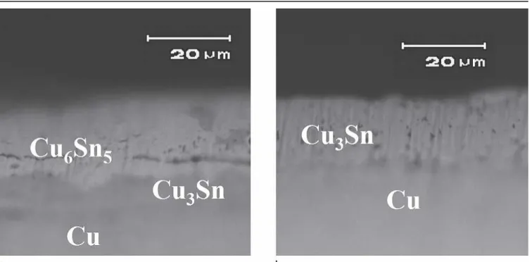
In order to grow a uniform Cu-Sn IMC layer, elec-troplating was used to make an even tin layer on cop-per substrates with dimensions of 1.5 cm 3 1.5 cm 3 0.050 cm. After the soldering reaction and anneal-ing, there existed two phases of Cu-Sn IMC: Cu6Sn5 and Cu3Sn. For the sample of Cu6Sn5, about 38 mm of tin was electroplated on the copper substrate for 25 min. For the Cu3Sn sample, in order to grow a layer of Cu3Sn without Cu6Sn5, a thinner tin layer of 20 mm was electroplated. The thinner tin layer shortened the time needed to make all of the Cu6Sn5 transfer to Cu3Sn. After a solid-state soldering reac-tion at 220°C for 80 hr and annealing at 325°C for 60 hr, the Cu6Sn5 sample had a layer of IMC with 16-mm Cu6Sn5and 10-mm Cu3Sn, which is shown on the left in Fig. 5. In the Cu3Sn sample, almost all of the Cu6Sn5 was transferred to Cu3Sn, as is shown on the right of Fig. 5. The procedure to remove the solder was the same as that for the Cu-Zn samples. The only difference was that the final polishing par-ticle size was reduced to 0.05 mm. With the nano-indentor, average values of the elastic moduli were determined to be 124 GPa for Cu6Sn5and 143 GPa for Cu3Sn.
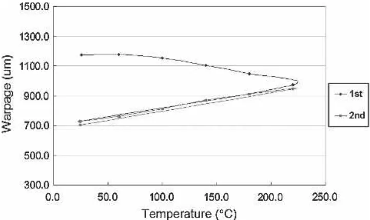
The warpage change of the two-layer structure with 9.8-mm Cu3Sn and 52.6-mm copper foil under temperature change was adopted for the CTE of the Cu3Sn. The dimensions of the sample were 3.0 cm 3 2.0 cm. In the tensile experiment, a strip of 5.5 cm 3 1.0 cm 3 80 mm copper foil with one end fixed was used. The tensile loading was applied to the other end by a force gauge. With a strain gauge in the middle of the specimen, the elastic modulus of cop-per foil was determined to be 100 GPa. Instead of reflection moire´, which has better resolution, shadow moire´ was applied because the initial deformation of such a thin foil is too large for the depth of field (DOF) of reflection moire´, and the sample was too flexible to form a good-quality reflective surface. With proper design of the dimensions of the speci-men, the resolution of shadow moire´ is sensitive enough to serve the purpose. The warpage of the sample was measured at room temperature, 60°C, 100°C, 140°C, 180°C, and 220°C in the oven with shadow moire´. The first measurement did not show monotonic change of warpage with increasing tem-perature. After cooling for 24 hr, the measurement was carried out again, and the relation between warpage and temperature became linear (as shown in Fig. 6), because the initial state of the sample had accumulative residual deformation, such as reflow from the temperature for IMC annealing and sam-ple trimming. In the first thermal loading, release of the residual stress did not allow the warpage to follow the increasing temperature. Finite-element analyses using ANSYS were applied to the Cu3Sn/ copper foil composite structure under changing tem-perature. The genetic search algorithm was used to optimally obtain the CTE of the Cu3Sn, which made the deviation between the measured and ANSYS-calculated warpages minimal. The CTE of the Cu3Sn
was determined to be 18.2 ppm/°C, which is approx-imately 10% greater than that of copper. Figure 7 shows that the experimental results were in good agreement with the finite-element model. We focused on the material properties of Cu3Sn instead of those of Cu6Sn5 because its interface with the thin metal layer is usually where the failure happens.
Ni-Sn Intermetallic Compounds
As for the Ni3Sn4 IMC, tin layers 40 mm thick were electroplated onto the nickel substrate. After a soldering reaction at 220°C for 80 hr and anneal-ing at 325°C for 93 hr, the tin was exhausted, and a layer of Ni3Sn4about 45 mm thick had formed. The morphology of Ni3Sn4 shows it has a much more even interface than Cu-Sn IMCs, as can be seen in Fig. 8. The post-processing was exactly the same as that for the Cu-Sn IMC, and the elastic modulus was determined to be 152 GPa. This 1-mm-thick nickel substrate was also tested with the nanoin-dentor to determine the elastic modulus, which was determined to be 213 GPa and consistent with the general value.
DISCUSSION
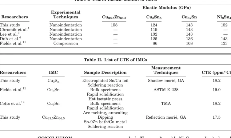
The list of the elastic moduli of IMCs, together with the results in the literature, is shown in Table I.
It is difficult to compare the results from nanoinden-tation with Fields’ results because the samples used by Fields were produced with a hot isostatic press instead of an actual solder joint, and the experimen-tal technique was also different.11 This study presents the same elastic modulus of Cu3Sn as that in most of the literature in which nanoindentation was applied, and the elastic modulus of Cu6Sn5falls in the average of all the values reported in the liter-ature. On the basis of the consistent results for Cu3Sn and Cu6Sn5, the data on Cu33.5Zn66.5 and Ni3Sn4can be considered reliable in this study.
Table II lists the CTEs of IMCs in the literature, and the sample preparation is also described. The records of the CTEs of IMCs are limited, and we have not found reports in which IMCs were adopted directly from soldering reactions so far, except for this study. The CTE of this study is in good agree-ment with that of bulks measured with other methods.11,12The proportional intensity of x-ray dif-fraction (XRD) for Cu3Sn is shown in Fig. 9. The Cu3Sn from copper foil in this study is consistent with the distribution of that from bulk in the data-base, which also reveals the reason that the CTE and elastic modulus of Cu3Sn in this study match the records in the literature well. The correspond-ence between the out-of-plane elastic modulus of Cu3Sn obtained with nanoindentation in this study and the in-plane ones in the literature is also con-sistent with the bulk properties illustrated with the XRD data. According to the results presented above, the methodology developed in this study for CTE measurement of IMCs is competent and successful. From the results of this study for Cu3Sn vs. cop-per, there is no severe difference in elastic moduli and CTE between the IMC and the metal substrate. It is probably other material properties that have a dominant effect on the failure of the interface between the IMC and the substrate. Hardness and toughness are potential candidates. From the results of Chromik, the hardness of copper is 1.7 GPa, and that of Cu3Sn is 6.2 GPa.1Hardness inhomogeneity might cause stress concentration at or near the interface between the IMC and the metal substrate or solder. In addition, brittle IMCs with low toughness near the interface where stress concentrates have a tendency to initiate or propagate cracks.
Fig. 8. Cross section of Ni3Sn4. Fig. 6. Warpage vs. temperature of Cu3Sn/copper foil structure.
Fig. 7. Warpage change from the experiment and finite-element analysis under unit temperature change (°C).
CONCLUSION
We have presented a new method for obtaining the CTEs of IMCs formed at the interface between lead-free solders and substrates. To successfully determine the CTE using the method developed in this study, the first challenge is to produce a flat and uniform layer of IMC on the substrate, and the area needs to be large enough to suit the resolution of the metrology methods adopted. Dipping for Sn-9Zn and electroplating for Sn were used to fulfill this pur-pose. To measure the deformation responses, we also developed an artificial cross grating for reflec-tion moire´ to overcome the problems of measure-ment under temperature change while preserving the improved resolution and the two orthogonal slopes. A nanoindentor was applied to determine the elastic moduli of Cu33.5Zn66.5, Cu6Sn5, Cu3Sn, and Ni3Sn4, with the assumption that Poisson’s ratio was 0.3 for all samples. The results with Cu6Sn5 and Cu3Sn agreed well with those of pre-vious publications in which nanoindentation was
applied. The results with Ni3Sn4 are limited, and those with Cu33.5Zn66.5 from Sn-9Zn are new. The CTE of Cu33.5Zn66.6was found to approximate that of copper. The deviation was within the resolution of the phase-shifting reflection moire´ using the method developed in this study. On the other hand, with the phase-shifting shadow moire´ and the search algorithms developed in this study, we also obtained the CTE of Cu3Sn, which was approximately 10% larger than that of copper and also consistent with that of the bulk specimens in the literature. The XRD result also matched that of the bulk specimens in the database.
ACKNOWLEDGEMENT
The authors sincerely acknowledge the financial support from the National Science Council, Taiwan, for this research (Grant NSC-94-2216-E002-015). The authors thank the Nano Center for Science and Technology, National Taiwan University, for permission to use the nanoindentor. The work was also partially supported by VIA Technology, Inc., ROC, and the Electrical Research Service Organiza-tion (ERSO) of the Industrial Technology Research Institute (ITRI), Taiwan, ROC.
REFERENCES
1. R.R. Chromik, R.P. Vinci, S.L. Allen, and M.R. Notis, J. Mater. Res. 18, 2251 (2003).
2. J.S. Kang, R.A. Gagliano, G. Ghosh, and M.E. Fine, J. Electron. Mater. 31, 1238 (2002).
Table I. List of Elastic Moduli of IMCs
Researchers ExperimentalTechniques
Elastic Modulus (GPa)
Cu33.5Zn66.5 Cu6Sn5 Cu3+Sn Ni3Sn4
This study Nanoindentation 158 124 143 152 Chromik et al.1 Nanoindentation — 119 143 —
Lee et al.3 Nanoindentation — 132 143 —
Duh et al.4 Nanoindentation — 125 136 143
Fields et al.11 Compression — 86 108 133
Table II. List of CTE of IMCs
Researchers IMC Sample Description MeasurementTechniques CTE (ppm/°C) This study Cu3Sn Electroplated Sn/Cu foil
Soldering reaction Shadow morie´, GA 18.2 Fields et al.11 Cu
3Sn Bulk specimens
Rapid solidification Hot isotatic press
ASTM E 228 19.0
Cotts et al.12 Cu
3Sn Bulk specimens
Rapid solidification Are melting, annealing
TMA 18.2
This study Cu33.5Zn66.5 Dipping
Sn-9Zn bath/Cu metal Soldering reaction
Reflection morie´, GA 17.5
3. M. Lee, Y. Hwang, M. Percht, J. Park, Y. Kim, and W. Liu, 2004 Electronic Components and Technology Conf. Proc. (Piscataway, NJ: IEEE, 2004), pp. 901–905.
4. G.Y. Jang, J.W. Lee, and J.G. Duh, J. Electron. Mater. 33, 1103 (2004).
5. C.A. Sciammarella, Exp. Mech. 22, 418 (1982). 6. A. Asundi, Exp. Mech. 34, 230 (1994).
7. I. Tsai, C.Z. Tsai, E. Wu, and C.A. Shao, Proceedings of IMAPS Taiwan Technique Symposium (Washington, D.C.: IMAPS, 2001), pp. 290–297.
8. F.P. Chiang, Exp. Mech. , 377 (1972).
9. Image Processing Toolbox User’s Guide (Natick, MA: The MathWorks, Inc., 1997).
10. K. Creath, Prog. Opt. 26, 351 (1998).
11. R.J. Fields, S.R. Low III, and G.K. Lucey, Jr., The Metal Science of Joining, ed. M.J. Cieslak, J.H. Perepezko, S. Kang, and M.E. Glicksman (Warrendale, PA: TMS, 1992), pp. 165–173.
12. N. Jiang, J.A. Chromik, and E.J. Cotts, Scr. Mater. 37, 1851 (1997).