I
Student Paper1
Modeling a n d Simulationof
High-bandwidthSi-based MOSlSOI
PhotodetectorsC.-Y. Liang’,
B.-C.
Hsub,C A .
Linb, S.T.
Change, and C. W. Liub ‘Graduate Institute of Electro-Optical Engineering, National Taiwan University,Taipei, Taiwan, R. 0. C.
Department of Electrical Engineering and Graduate Institute of Electronics Engineering, National Taiwan University, Taipei, Taiwan, R. 0. C.
’
Department of Electronic Engineering, Chung Yuan Christian University, Chung-Li, Taiwan, R. 0. C.Tel: 886-2-2363525 I ext. 515 /Fax: 886-2-23638247 / E-mail: chee0cc.ee.ntu.edu.tw
The bandwidth of bulk-MOS photodetectors (PD) can not reach GHz due to the absorption length of 850 nm lightwave in Si (-22 um) is much larger than the Si depletion width even when the device is deeply depleted [1][2]. Therefore, most photo-generated electron-hole pairs are located in the bulk neutral region and are collected by gate electrode through the slow diffusion process. The large diffusion current seriously limits the device bandwidth and the applications. In this work, a novel MOS PD structure is proposed to eliminate the difliusion current by taking advantage of SO1 technology (Fig. I ) . The thick buried oxide stops the diffusion current from substrate and the thin absorption layer makes sure that the device is fully-depleted during operation. The absorption region and groond electrode are separated by oxide and connected by buffer layer. Note that the grid structure of AI gate electrode allows the light directly exposures on the absorption region. The device simulation is carried out by commercial software ISE [3].
Since the diffusion current is eliminated in SOI-MOS PD to increase device speed and bandwidth, total photocurrent is also reduced (Fig. 2). Thicker absorption region will increase the responsivity but reduces bandwidth if the absorption layer is thicker than the depletion width. Since the tunneling MOS diode is deep depleted under inversion bias (inset of Fig. 2), lighter doping in absorption region and higher operation voltage (V,) will increase the depletion width. Fig. 3 is the band diagram of SOI-MOS PDs along hole current path from oxide/Si interface to ground contact for devices with different buffer layer doping concentration ( I O N 6 ,
IO”,
andIO”
cm-I). Electron-hole pairs are generated in absorption layer and the holes are swept into buffer layer (flat band region) and finally collected by ground. The device with lOt6cm-’ doping has a energy barrier because the depletion width extends into the lightly doped buffer layer. Therefore, the photo-generated carriersin
the middleof
the device are blocked and couldn’t transport into ground contact. The transient analysis is also carried out and shows the same results (Fig. 4). The photocurrent of device with IOzo cm” buffer layer doping rises and falls quickest under 5 ps optical impulse due to the smallest resistivity and RC delay time. Note that when devices are operated in high speed, the SOI-MOS PD generates more photocurrent than the bulk device, unlike the result in DC condition (Fig. 2). The inset of Fig. 4 shows the experimental result of a typical bulk MOS PD with 2 ns FWHM.The frequency response model of SOI-MOS PDs is also derived. By considering the grid structure of AI gate electrode and the device symmetry, photo-generated carriers are divided into
three
regions (Fig. 5). Carriers in the three regions have the same transport time within absorption region but different depletion capacitance and series resistance in buffer layer. The total frequency response is obtained by linearly adding them together, as shown in Fig. 6 [4]. The analytical model precisely fits the computer simulation results (Fig. 7). The bandwidth o f the MOS/SOI PD is up to 22 GHz. The parameter values used in the analytical model are given in Table. I . For device with I O a 6 buffer layer doping, the efficiency is only 115 as compared to other devices because the ground contact only collects the hole generated in the outer part, where the area is 115 of the total active area. In DC condition, however, the carriers generated in the middle part can transport to ground contact, so the DC photocurrent are the same for all devices (inset of Fig. 7.).In conclusion, the novel SOI-MOS PDs can have high bandwidth (22 GHz) and are fully compatible with ULSI technology. The device structure could be optimized by tuning the doping and thickness of epi-layers. The absorption layer can be Si, SiGe and quantum structures to extend the device detection wavelength to 1.3, 1.5 pn and even for I O W infrared detection. [I]
B.-C.
Hsu et al., IEEE EIecnon Device Letters, vol. 24, pp. 3 18-320,2003.121 B.-C. Hsuetal.,/EDMTech. Dig., pp.91-94,2002.
[3] ISE TCAD 8.0. [4] Weishu Wu et al., J. OfLighhVave Tech., vol. 14, pp. 2778-2785, 1996.
\,
230Fig I The prop~sed SOI-MOS PD smmc The
absorption layer IS fully-depleted d m g opsrat~on
Notc that lhcrc IS no ham gsncraoon and photo cumcnt
under A I mnfaCt k c a w OfrCfleCbon
c
camcr Tnnlport path [ a U. )
Fig. 3 Band diagram of the Sol-Mos PD5 with
different buffcr laysr doping. The 1 ~ 5 1 shows the mute
of hole Current A snsrey bamsr
_.
for hole IS ohsewed fordsvicc with 10" buffer layer doping.
\ ' E
Fig. 5 The "ght half side of SO1 PD is divided by AI
contaels into Uvsc regions. Current in each region has ils
own depletion cBpacifMss. xticr ~sisfance and
frquEncy TCIPOme. 1 I .I I 1G IOG 22G l O D G Frequency ( H1 ] U m-111 '0".
FBg 2 The dark and photo m n t of bulk and SO1
dcviccs under 850 nm light cxparurc The mist shows that
under inv~r~ion bias (VpO), most voltage dmpr falls on St
subshatc and the dcplstion width tncrcases wth V,
' " " . , , , . 6 5 4 3 4 - i 0 1 2 , , G a l e Voltage ( v )
I
0 10 20 30 40 Time ( ps )Fig. 4 Transient analysis of SO1 dcvicer with 5 p i optical
impulw. T h c device with lughut buffer layer doping h
sbrlest falling time and largest pholoFimcnl. The inset
s h o w h t the bulk dcvlee has B 2 N FWHM measured
which is much lager lhan thc plot scaIc.
Fig. 6 The proposed analytical s o I ~ f i ~ l l ~ far MOS/SOI
Photodetectors. C and R M h ~ t i o ~ of width of AI
cOntaCl and space bclwecn AI ~ o n f a ~ l s .
Fig. 7 Frequency ~ C I P O N F S of dmiws with different buffer
Iaycr doping canssntration. Ths dwms with higher doping
conccnlraImn yields larger bandwidth. The rficicncy of
doping 10" dcvicedmps near DC bec~wc lhc buffer layer is
alra depleted and most holes are blocked by the energy bamrr
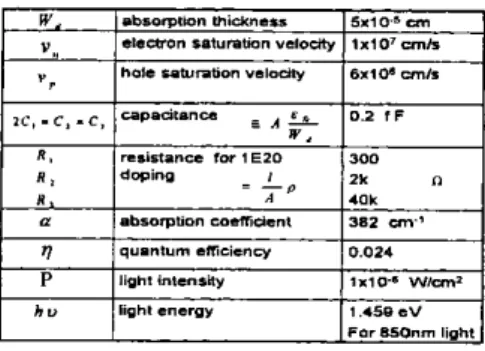
Table I . Parametor values wed nn analytical solution. The
resismce values am only for the dcvics with 10" buffer
layer doping.