一種分析薄膜電晶體內完整能帶隙態位密度分佈的新穎方法
87
0
0
全文
(2) 一種分析薄膜電晶體內完整能帶隙態位密度分佈的新穎方法 A NOVEL METHOD TO ANALYZE FULL BAND-GAP DENSITY OF STATES DISTRIBUTION IN THIN FILM TRANSISTORS. 研 究 生:蘇育正. Student: Yu-Cheng Su. 指導教授:黃調元 博士 Advisor: Dr. Tiao-Yuan Huang 指導教授:林鴻志 博士 Advisor: Dr. Horng-Chin Lin. 國立交通大學 電子工程學系 電子研究所碩士班 碩士論文. A Thesis Submitted to Institute of electronics College of Electrical Engineering and Computer Science National Chiao-Tung University in Partial Fulfillment of the Requirements for the Degree of Master in Electronics Engineering June 2004/6/8 Hsinchu, Taiwan, Republic of China. ii.
(3) 一種分析薄膜電晶體內完整能帶隙態位密度分佈 的新穎方法. 研究生:蘇育正. 指導教授:黃調元 指導教授:林鴻志. 博士 博士. 國立交通大學 電子工程學系. 電子研究所. 摘. 要. 在本篇論文中,我們提出一種創新的分析薄膜電晶體通道層內能 帶隙態位密度(DOS)分佈的方法,利用此方法我們可以在單一元件中 一次求得全能帶隙的態位密度分佈,不僅簡化量測與分析程序,同時 也大幅降低製造成本與分析時間。. 傳統若要求得全能帶隙缺陷密度分佈,必須分別製作 N 型和 P 型 的薄膜電晶體才能獲得。在本論文中,我們利用一種具有電場感應汲 極之蕭特基薄膜電晶體元件,可以實現完整能帶隙之薄膜態位密度分 析。由於電場感應汲極之蕭特基薄膜電晶體在靠近汲極端有一電性接 面(electrical junction)區,利用其上方的副閘極的偏壓可以感應 出不同極性的電性接面,並藉此使單一元件可變換地操作在 N 或 P I.
(4) 通道模式。利用此一雙向操作(ambipolar)能力,再結合場效電導 (field effect conductance)法,可以在單一元件中求出費米能階 上、下的完整能帶隙缺陷密度分佈,而不必分別製作 N 及 P 通道模式 的元件,如此將可大幅降低製作成本,並增加分析便利性。. 此外,我們也在實驗中發現,在室溫下量測 N 通道和 P 通道的源 極電流與閘極電壓特性,其交叉點的閘極電壓與傳統利用變溫方法求 得的平帶電壓(flat-band voltage)幾為一致。經由實驗中不同製程 與結構的元件一再的比對,均證實此現象的存在,因此我們提出利用 此方式量測通道層內的平帶電壓,如此將可避免傳統變溫方法的耗時 與繁複,大幅簡化程序並節省時間。. 利用此方法,我們可以分析在不同的製程條件下薄膜的缺陷密度 分佈。由於薄膜電晶體的電特性強烈受到通道中缺陷態位密度的影 響。因此,透過我們提出的方法,能讓我們對薄膜電晶體的元件特性 有更深入的瞭解,也有助於業界量產所須對薄膜電晶體元件的模式分 析及電路設計與模擬的工作。. II.
(5) A novel method to analyze full-band gap state density distribution in thin film transistors Student: Yu-Cheng Su. Advisor: Dr. Tiao-Yuan Huang Advisor: Dr. Horng-Chin Lin. National Chiao-Tung University. Abstract In this thesis, we propose a novel method to acquire the full band-gap density-of-state (DOS) in the channel layer of a thin-film transistor (TFT). In this new approach, only a single Schottky barrier thin-film transistor (SB-TFT) device is characterized, in contrast to the conventional methods that require both n- and pchannel devices for characterization. In a SB-TFT with field-induced drain (FID), an electrical drain junction is set between the channel portion underneath the main-gate and the metallic drain. A sub-gate lying above the electrical drain junction is used to adjust the polarity and resistance of the electrical junction, enabling the ambipolar operation of the device. Field-effect conductance (FEC) method is applied to analyze the ambipolar subthreshold current-voltage characteristics and acquire full band-gap DOS. Experimentally, we have also observed that the gate voltage at the intersection point of n- and p-channel subthreshold current-voltage characteristics coincides well III.
(6) with the flat-band voltage measured using the conventional temperature method. We thus propose to exploit this new finding, in lieu of the conventional method, to extract the flat-band voltage, which further simplify our methodology, as only two current-voltage measurements at room temperature are needed for the construction of full band-gap DOS. Our proposed method has been demonstrated to be useful on characterizing and understanding the impacts of different process treatments on the device characteristics. Accompanied with its simplicity and significant saving of both analysis cost and time, this method could be vital to TFT device modeling and circuit simulation works for both R&D and practical manufacturing.. IV.
(7) 誌謝 在碩士班的兩年中,有許多的人需要感謝,首先就是我的指導教授老 師黃調元博士和林鴻志博士,黃老師的豐富教學經驗讓我學到許多東西,林博認 真、嚴謹的指導,也讓我的碩士論文更加豐富、完整,在交大的豐富教學資源和 兩位老師的指導之下讓我在這兩年能有所收穫,不至有入寶山空手而回的遺憾, 此外也要感謝帶領我畢業的葉冠麟學長、和曾經帶過我的李耀仁學長,在他們不 厭其煩回答我的困惑之下,讓我解決了許多問題,也讓我能順利的畢業,另外也 感謝實驗室學長,如:盧文泰學長、呂嘉裕學長、李明賢、林宏年、歐士傑,都 曾給予我許多幫助,實驗室同學盧景森、蘇俊榮、林柏青、林盈彰和我一起度過 兩年學習的過程,讓我在這兩年中有許多歡樂,另外也感謝陪伴我度過碩士生涯 的女友螢聖,在這兩年中陪著我度過每一個開心、難過的日子,最後要感謝我的 父母和家人在這兩年給我精神上、實質上的鼓勵和幫助,讓我能無後顧之憂的完 成碩士學業。. V.
(8) Contents Abstract (in Chinese)…………………………………………………………….Ⅰ Abstract (in English)……………………………………………………………..Ⅲ Acknowledgement……………………………………………………………….Ⅴ Contents………………………………………………………………………….Ⅵ Table captions……………………………………………………………………Ⅷ Figure captions………………………………………………………………......Ⅸ List of symbols………………………………………………………………….XII. Chapter 1. Introduction. 1.1 Background and motivation……………………………………………1 1.2 Thesis outline…………………………………………………………..2. Chapter 2. Realization of Full Band-Gap DOS Analysis Using A Single Device. 2.1 Field effect conductance method……………………………..………...4 2.2 Operation of ambipolar TFT…………………………….…….……….7 2.3 Device fabrication…………………………………………………..….8. Chapter 3 Analysis of Full Band-Gap DOS in FID-SB TFT Structure 3.1 Determination of DOS using the temperature and incremental methods……………………………….…………...…………………..11 VI.
(9) 3.2 Effect of applied drain bias…………………….………………………….13 3.3 Effects of channel length………………………….....…………………….13 3.4 Effects of drain side extension length……………………………………..14 3.5 Effects of measurement temperature……………………...…….…………14 3.6 Results comparison with conventional approach…………....…………….15 3.7 Effects of channel crystallization treatment………………..….…………..15 3.8 Effects of plasma hydrogenation………………………...………………...16 3.9 Effects of silicide material……………………………………….………...17 3.10 Analysis of full band-gap DOS in SB poly-Si FinFET…………..………17 3.11 A new & simpler methodology to determine flat-band voltage……….19. Chapter 4 Conclusions and Future Work 4.1 Conclusions………………………………………………...………………21 4.2 Future work………………………………………………………………...22. VII.
(10) Table Captions Table.1 The extracted device parameters of CoSi2 Source/Drain material.. Table.2 Gap state density of different channel films.. VIII.
(11) Figure Captions Fig.2.1 1-D Band scheme of a gate-oxide-poly-Si channel structure. x is 0 at the oxide/poly-Si interface. Fig.2.2 Flow chart for determination of DOS using conventional approach. Fig.2.3 (a) Self-aligned cross section of FID SB-TFT. Fig.2.3 (b) Non self-aligned Cross section of FID SBTFT. Fig. 2.4 The fabrication flow of FID SBTFT. Fig.3.1 Flat-band voltage determination of FID SB-TFT using Tx(dlogG/dVG) vs. 1/T plots: (a) n-channel operation; (b) p-channel operation. Fig.3.2 Full band-gap DOS distribution extracted using the FID SB-TFT. Fig.3.3 Drain current versus gate voltage characteristics. Fig.3.4 Log(dG/dVG) versus 1000/T. Fig.3.5 Activation energy versus gate voltage characteristics. Fig.3.6 Full band-gap DOS deduced by the incremental method and the temperature method. Fig.3.7 Ambipolar transfer characteristics in both low and high drain bias. Fig.3.8 Full band-gap DOS extracted at |VDS| of 0.1 and 5 V. Fig.3.9 (a) Ambipolar transfer characteristics and (b) the extracted. DOS results in a. device with channel length of 0.8um. Fig.3.10 (a) Ambipolar transfer characteristics and (b) the extracted DOS results in a device with channel length of 1um. Fig.3.11 (a) Ambipolar transfer characteristics and (b) the extracted DOS results in a device with channel length of 2um. Fig.3.12 (a) Ambipolar transfer characteristics and (b) the extracted DOS results in a device with channel length of 5um.. IX.
(12) Fig.3.13 On current vs. channel length. Fig.3.14 (a), (b) Comparison of DOS extracted in devices with various channel length. Fig.3.15 (a) Ambipolar transfer characteristics of deices with various drain-side offset length at |VDS| of 0.1 V.. (b) Full-band gap DOS extracted deices with various drain-side offset length at |VDS| of 0.1 V. Fig.3.16 (a) Ambipolar transfer characteristics of deices with various drain-side offset length at |VDS| of 5 V. (b) Full-band gap DOS extracted devices with various drain-side offset length at |VDS| of 5 V. Fig.3.17 Ambipolar transfer characteristics measured at 25 and 55 oC. Fig.3.18 DOS extracted at 25 and 55 oC. Fig.3.19 Comparison of DOS extracted from FID SB-TFT and Conventional TFTs. Fig.3.20 Full band-gap DOS of devices with SPC or as-deposited poly-Si channel. Fig.3.21 TEM micrographs of device with (a) as-deposited poly-Si and (b) SPC channel film. Fig.3.22 Full band-gap DOS of devices with SPC or ELA poly-Si channel. Fig.3.23 (a) TEM micrograph of SPC channel film. Fig.3.23 (b) TEM micrographs of ELA channel film. Fig.3.24 Ambipolar transfer characteristics of devices with and without plasma treatment. Fig.3.25 Full band-gap DOS before and after hydrogenation in devices with SPC channel. Fig.3.26 Full band-gap DOS before and after hydrogenation in devices with as-deposited poly-Si channel. Fig.3.27 Ambipolar transfer characteristics of a device with PtSi S/D. Fig.3.28 Full band gap DOS of devices with CoSi2 or PtSi S/D. Fig.3.29 (a) Top view of poly-Si SB FinFET with self-aligned spacer; (b) Top view of X.
(13) poly-Si SB FinFET with offset region XD and XS. (c) Cross section view along A-A+ direction in (b); (d) Cross section view along B-B+ direction in (b). Fig.3.30 Ambipolar transfer characteristics of a SB poly-Si FinFET. Fig 3.31 Higher sub-gate bias enhances the source-side field emission. Fig.3.32 Ambipolar transfer characteristics of SB poly-Si TFT with planar structure. Fig.3.33 Ambipolar transfer characteristics of a SB poly-Si FinFET. Fig.3.34 (a) Ambipolar transfer characteristics of a SB poly-Si FinFET measured at varying temperature, (b) Flat band voltage determination. Fig.3.35 Full-band gap DOS of planar SB -TFT and SB FinFET. Fig.3.36 Comparison of flat-band voltage determined by conventional temperature method and our new method. Fig.3.37 Modified Flow chart for determination of DOS density.. XI.
(14) List of symbols E. Energy. d. Polysilicon thickness. EF. Fermi energy. k. Boltzmann constant. n. electron concentration. n0. Equilibrium electron concentration. Ng(E). Density of gap states (DOS). q. Electronic charge. tox. Gate dielectric thickness. Xo. Unmodulated bulk length (or depletion width in the channel). k. Boltzmann constant. T. Temperature (K). VFB. Flat band voltage. VG Vth. Gate voltage Threshold voltage. εox. Gate dielectric constant. εsi. Silicon dielectric constant. μ. Electron mobility. ψ. band bending. ψs. surface band bending of the channel. ρ. charge density. G. conductance. G0. conductance at flat band condition. XII.
(15) Chapter 1 Introduction. 1.1 Background and motivation Thin-film transistors (TFT), which employ a thin semiconductor film on an insulating substrate as the active device channel, was first demonstrated in 1961 by Dr. P. K. Weimer in RCA. With its simplicity in structure and fabrication, applications of thin-film transistors in image sensors and displays become more and more popular. Interest in low temperature poly-Si TFT has been growing rapidly over the last decade. This is due to a much higher mobility and drive current of poly-Si TFTs, compared to amorphous Si counterparts, which enables the integration of peripheral circuits on the same panel in active matrix liquid crystal displays (AMLCD) manufacturing [1]. The electrical properties of polycrystalline semiconductor devices are strongly affected by defects such as dangling bonds and strained bonds located at the grain boundaries [2-3]. An understanding of the nature, energy distribution, density, and behavior of these defects is important for the development of polycrystalline TFTs. Several approaches have been developed to determine the density of gap states (DOS) in polycrystalline devices, such as capacitance-voltage method [4], the doping dependence of conductivity [5], and the field effect conductance (FEC) method [6-7]. Among them, only the field effect conductance method is compatible with modern poly-Si TFT samples. A theoretical interpretation of the field effect conductance method was given by Suziki et al [8] to calculate the DOS of amorphous Si TFTs [9]. The technique has been extensively applied to a-Si:H devices and provides adequate information on the DOS in spite of some interpretation difficulties, such as the. 1.
(16) differentiation between bulk and interface states. In the case of poly-Si TFTs, the method has also been proven to be sensitive enough to account for the effect of film morphology and differences in device processing [10]-[11], thereby providing an essential tool for the analysis of poly-Si thin film transistors. However, there are also several issues associated with the field-effect conductance method. In particular, the distributions of gap states in upper (Ei ~ Ec) and lower (Ei ~ Ev) half of band-gap are obtained using n- type and p- channel devices, respectively. This limitation necessitates the use of at least two separate devices with different channel types to obtain full band-gap density of state analysis. Moreover, measurements need to be performed at various temperatures in order to determine the flat-band voltage (for details, please refer to the method description in the next chapter). In this work, we propose a novel method to determine the full band-gap density of states of poly-Si channel using only a single device. The new method is successfully demonstrated on a novel Schottky barrier (SB) TFT device with field-induced drain (FID) that our group has developed previously [12]-[16]. The SB-TFT device exhibits an ambipolar operation capability, i.e., both n- and p- channel operation modes could be achieved in a single device. By exploiting this unique characteristic, we can perform the field effect conductance method to acquire the full-band gap state density distribution using only a single device. Experimentally, we also found that the flat-band voltage could be acquired by simply characterizing the ambipolar current-voltage (I-V) characteristics, without resorting to various temperature measurements. The extracted value is very close to that obtained by the temperature method, while the measurement scheme is greatly simplified.. 2.
(17) 1.2 Thesis outline This thesis is organized as follows: In Chapter 2, theoretical background of the FEC analysis, operation principles and the fabrication of the FID SB-TFT are described. Firstly, we introduce the theory of using the field-effect conductance to determine the gap state density used in conventional poly-Si TFT. Secondly, ambipolar operation of the FID SB-TFT is presented. Thirdly, the device fabrication flow is described. In Chapter 3, experimental results are presented and discussed. Special attentions are paid to the determination of the flat-band voltage, and the effects of applied bias, recrytallization methods, hydrogenation, and the silicide materials. Finally, we summarize our achievements and give conclusions in Chapter 4.. 3.
(18) Chapter 2 Realization of Full Band-Gap DOS Analysis Using A Single Device. 2.1 Field Effect Conductance Method As mentioned in the last chapter, the performance of poly-Si TFTs is strongly affected by defects in the poly-Si channel. Characterization and analysis of DOS is thus essential for understanding the device characteristics as well as its dependence on the processing conditions. Moreover, accurate DOS is required for the modeling of poly-Si TFT characteristics. It has been shown that field effect conductance (FEC) method can serve this purpose. In this chapter, we will first briefly review its theoretical background. FEC method was original proposed for characterizing the DOS in a-Si TFTs. When applied to poly-Si TFTs, the presence of grain boundaries in the channel could be of great concern. Fortunately, it has been proven that, when the grain size is small enough (compared to the channel length), the poly-Si channel film can be modeled using the “ effective-medium " approach [6], in which the existence of grain boundary defects and intragranular defects are assumed to be uniformly distributed throughout the material. Under this assumption, the band bending is a solution of the one-dimensional Poisson’s equation.. ρ (χ ) d 2ψ | =− 2 x=0 ε Si dx. (2-1). The meanings of the symbols could be found in the List of Symbol (page [XII]). ρ(x), charge density per unit volume, can be expressed by. 4.
(19) Ec. Ec. Ev. Ev. ρ (ψ ) = − q ∫ Ng ( E ) f ( E − E F − qψ )dE + q ∫ Ng ( E ) f ( E − E F )dE. (2-2). The first term denotes acceptor-like states, which are neutral when empty and negatively charged when filled with electrons. The second term denotes donor-like states, which are positively charged when empty and neutral when filled with electrons. For sufficiently low temperatures, all states below the Fermi level are filled and all states above the Fermi level are empty. Eqn. (2-2) can be written (zero-temperature approximation):. ρ (ψ ) = − q. E F + qψ. ∫ Ng ( E )dE. (2-3). EF. where Ng(E) is the gap-state density (per unit volume). Multiplying by 2 ⋅ ∂ψ / ∂x and integrating from x=0 (oxide-semiconductor interface) to x=Xo (unmodulated bulk, see Fig. 2.1): 2. ψ. 2q s ⎞ ⎛ dψ | x =0 ⎟ = dφ ⎜ ε Si ∫0 ⎠ ⎝ dx. E F + qψ. ∫ Ng ( E )dE. (2-4). EF. ⎛ dψ ⎞ where ψs is the band bending at x=0 (surface potential) ,and ⎜ | x =0 ⎟ is the ⎝ dx ⎠. electric field at the surface. The gap-state density is then given by. ε ∂ 2 ⎛ dψ ⎞ Ng ( E F + ψ s ) = Si | x =0 ⎟ 2 ⎜ 2q ∂ψ s ⎝ dx ⎠. 2. (2-5). The electric field at the semiconductor surface is given, in the absence of surface states,. ε V ε V − VFB − ψ S dψ | x =0 = − ox ⋅ ox = − ox ⋅ G dx ε Si t ox ε Si t ox. (2-6). From Eqns. (2-5) and (2-6), the gap-state density can be determined if the relationship between VG and ψs and bulk Fermi energy are known. The relationship between VG and ψs can be determined by the following two methods. 5.
(20) The incremental method By assuming that the transport is by electrons, the field conductance is defined as [8]. G G = G0 − 0 d. ψs. exp(qψ / KT ) − 1 dψ dψ / dx 0. ∫. (2-7). where d is the poly-Si film thickness and Go is the conductance for the flat band condition. The conductance is defined as the derivative of drain current with respect to the gate voltage at a fixed drain voltage. Differentiating Eqn. (2-7) with respect to the surface potential gives. G exp(qψ / KT ) − 1 dG =− 0 ⋅ dψ s d dψ / dx | x =0. (2-8). By substituting Eqn. (2-6) into Eqn. (2-8), the following approximation expression is obtained: dψ s VG − VFB − ψ s 1 ε 0x d = ⋅ ⋅ ⋅ dG G0 ε Si t0 x exp( qψ s / KT ) − 1. (2-9). Actually, Eqn. (2-9) can be expressed by the differential form:. ψ s ,i +1 = ψ s ,i +. Gi +1 − Gi d ε 0 x VG ,i − V FB − ψ S ,i ⋅ ⋅ ⋅ G0 t 0 x ε Si exp( qψ S ,i / KT ) − 1. (2-10). which can be used to construct the ψs against VG relationship.. The temperature method This method is based on the temperature dependence of dG/dVG . From Eqns. (2-8) and (2-6), and dG/dVG=(dG/dψ S )(dψ S /dG), one can obtain the following expression:. dG. dVG. = G0. ε 0x d Si ⋅ t 0 x. ⋅. exp[( E F − EC + qψ ) / KT ] ≡ k ⋅ e ( − ∆E / KT ) ρ (ψ s ). (2-11). Both EF andψs in the above equation are expected to be temperature dependent. This 6.
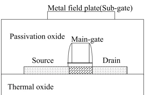
(21) dependence is due to the variation of Eg with T and to the so-called statistical shift. The latter is due to the fact that the total density of electrons (trapped plus free electrons) is a constant, so that Eg must shift with T in order to compensate for the temperature dependence of the Fermi function. Since all terms on the right-hand side, with the exception of exp(qψs/kT), have a weak temperature dependence, ψs can be determined from log(dG/dVG) versus 1/T plot. The temperature analysis also allows the determination of an important parameter, namely, the flat band voltage. Following the method proposed by Weisfield and Anderson [17], the following expression is obtained for smallψs. 2 d log G ε 0 x 1 ⎡ 1 ⎛ qψ s ⎞ ⎛ qψ s ⎞ ⎤ ≅ ⋅ ⎟ + O⎜ ⎟ ...⎥ ⎢1 + ⎜ dVG t0 x qkTN 0 ⎢⎣ 2 ⎝ KT ⎠ ⎝ KT ⎠ ⎦⎥. (2-12). where No is the DOS at the Fermi level under flat band condition. VFB is then determined as the gate voltage where T(dlogG/dVG) is temperature independent. Fig. 2.2 summarizes the flow chart using conventional FEC scheme to determine the DOS. It should be noted here that both p- and n-channel devices are needed for full band-gap DOS characterization.. 2.2 Operation of Ambipolar TFT In this study we propose a new approach that utilizes only a single FID SB-TFT to achieve the full band-gap DOS characterization. Here we briefly describe the structure and operation of FID SB-TFT device. Cross-sections for two types of device are shown in Fig. 2.3. The device features metallic silicide junctions and a metal field-plate, also called sub-gate, lying over the passivation oxide. Offset regions in the channel are formed in both drain and source sides. It is the key to achieve excellent ambipolar characteristics without suffering from the severe off-state leakage. In this. 7.
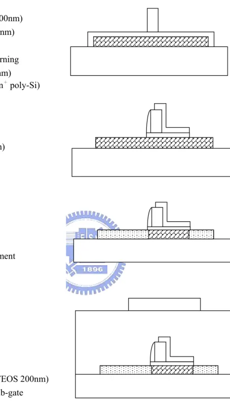
(22) study, the source-side offset region is defined by a self-aligned sidewall spacer, while the drain-side offset region is formed by either sidewall spacer or by an extra lithography step. In the latter case (Fig. 2.3 (b)), the length of the offset region, XD, is defined by the mask. In this work, most samples use Cosi2 as the source and drain material to exploit its near-mid-gap work function. With near-mid-gap work function, the barrier height between electrons and holes is comparable (Note: barrier height for electron is slightly higher than for hole in this case), resulting in near symmetrical I-V characteristics. Issues regarding the barrier height of silicde on the DOS measurement will be addressed in Chap. 3. During device operation, a proper fixed voltage is applied to the field-plate to form an electrical drain extension under the field-plate region. The device can be set for n- and p-channel operations with positive and negative biases, respectively. With appropriate bias and polarity applied on other electrodes (i.e., main gate, and drain), excellent ambipolar transfer characteristics could be achieved. The unique ambipolar characteristics are exploited in our approach to extract full band gap DOS using only a single device.. 2.3 Device Fabrication The key processing flow of the proposed structure is shown in Fig. 2.4. Detailed processing is described below.. ● Poly-Si channel deposition 1. Si wafers capped with thick thermal oxide were employed to serve as a substitution for the glass-like substrate used in the active matrix liquid crystal display (AMLCD).. 8.
(23) 2. An amorphous silicon channel layer (50nm) was deposited at 550oC by low temperature chemical vapor deposition (LPCVD). For some splits, as-deposited poly-Si was used instead. 3. The amorphous silicon layer was then transformed to polysilicon layer either by solid phase crystallization (SPC) method or excimer laser annealing (ELA). For the solid phase crystallization, wafers were re-crystallized at 600oC in N2 ambient for 24 hours.. ● Gate oxide formation 1. The active area was defined using a G-line stepper. 2. LPTEOS gate oxide (50nm) was deposited, followed by deposition of poly-Si gate layer (200nm). 3. The poly-Si gate layer was subsequently doped by arsenic ion implantation, and then activated in N2 ambient for 24 hours. 4. The n+ poly gate layer was then patterned to form the main gate.. ● Offset region definition 1. Deposition of LPTEOS oxide layer (200nm). 2. Photolithograhic and plasma etch steps were used to define the offset region.. ● Schottky source/drain formation The source/drain was formed by self-aligned silicidation (salicidation): 1. Sputter deposition of a thin Co layer (20nm) capped with TiN (30nm). 2. Rapid thermal annealing (RTA) was performed at 550oC for 30 seconds to form silicide. 3. The non-reacted metals were removed by selective wet etching (H2SO4: 9.
(24) H2O2=3:1 for 10 minutes at 120oC). 4. Deposition of plasma enhanced TEOS (PE-TEOS, 200nm) to serve as passivation oxide.. ● Contact hole and metal pad formation 1. A lithographic step was used to pattern 90x90μm2 contact holes. 2. Contact hole etching was performed in an ANELVA ILD-4100 dry etcher. 3. Sputter deposition of a 300nm Al film. 4. Patterning of metal pads. 5. Post metal annealing was performed at 400oC for 30 minutes in N2 ambient.. ● Plasma hydrogenation Wafers received a NH3 plasma treatment in a PECVD chamber for 1 hour at 250oC.. 10.
(25) Chapter 3 Analysis of Full Band-Gap DOS in FID-SB TFT Structure 3.1. Determination of DOS Using Temperature and Incremental Methods Figure 2.2 shows the flow chart for the determination of DOS used in field. effect conduction method. First of all, we have to obtain the flat-band voltage of the device. The flat band voltage can be determined by the temperature (i.e., activation energy) method with Equation (2-12) 2 d log G ε 0 x 1 ⎡ 1 ⎛ qψ s ⎞ ⎛ qψ s ⎞ ⎤ O ≅ ⋅ 1 + + ⎜ ⎟ ⎜ ⎟ ...⎥ ⎢ dVG t0 x qkTN 0 ⎢⎣ 2 ⎝ KT ⎠ ⎝ KT ⎠ ⎦⎥. (2-12). From the above equation, the flat-band voltage can be determined by the VG when the product Tx(dlogG/dVG) is temperature independent (because surface potential is zero). Figures 3.1 (a) and (b) show the characteristics of T x (dlogG/dVG) against 1000/T performed on a FID SBTFT under n- and p-channel operation modes, respectively. From the two figures, the flat-band voltage is determined to be around -2.1V that is almost independent of the temperature in either p- or n-channel operation. Once the flat-band voltage is obtained, the relationship between the gate voltage VG and surface potential φs could be established by either incremental method or the temperature method mentioned in Chap. 2. Next, we first use the incremental method to obtain this relationship, as shown below:. ψ s ,i +1 = ψ s ,i +. Gi +1 − Gi d ε 0 x VG ,i − V FB − ψ S ,i ⋅ ⋅ ⋅ G0 t 0 x ε Si exp( qψ S ,i / KT ) − 1. 11. (2-10).
(26) Here we use the Visual Basic Language to obtain the solution of this equation. After the flat-band voltage and the relationship between gate voltage and the surface potential are determined, Matlab language is adopted to obtain the gap-state density. Fig. 3.2 shows an example of the DOS versus energy level in the gap. In this case the channel is solid phase crystallization (SPC) poly-Si film. The channel width is 20um, and the channel length is 2um. The upper- and lower-half gap density is obtained by biasing the device into the n- and p-channel operation modes, respectively. Next, we show how the temperature method is performed to obtain the relationship between the gate voltage and surface potential. This method is based on the temperature dependence of conductance at different gate voltages. Figure 3.3 shows the characteristics of drain current versus gate voltage measured at different temperatures. It can be seen that the on-current becomes larger as the temperature gets higher, simply due to a higher thermionic emission. Figure 3.4 shows the Arrhenius plot of dG/dVG against 1000/T at different applied gate voltages. The slope of each straight line defines the activation energy, Ea. Figure 3.5 shows the characteristics of activation energy against gate voltage. As the gate voltage is increased, activation energy falls due to increasing carrier density (and thus lower barrier height). From the equation Ea= Ecb-EF0-qψs stated in Chap. 2 and the results obtained in Fig. 3.5, we can obtain the relationship between the gate voltage and surface potential. As a consequence, the gap-state density distribution could be obtained. Figure 3.6 shows and compares the DOS versus energy level in the gap obtained by the temperature method and incremental method. The results are in reasonable agreement with each other. Nevertheless, in most cases it is observed that the data obtained from the temperature method show more fluctuation in the mid-gap region. This is ascribed to the dramatically lowering in measured current as temperature is reduced. In some instances the current is close to or even below the limit of the measurement system. 12.
(27) Thus, it is preferable to use the incremental method, rather than the temperature method, to determine the relationship between the surface potential and gate voltage.. 3.2. Effect of Applied Drain Bias. Here we address the effect of drain bias on the measurement results. The measurements were carried out for n-channel operation by sweeping gate voltages from –3 to +6V, and for p-channel operation by sweeping gate voltages from –1 to –10 V, with drain voltages |VDS|= 0.1V or 5V, and sub-gate voltage |Vsub|=50V. Figure 3.7 shows the characteristics of the ID-VG for the FID SB-TFT with CoSi2 S/D material. The channel film is SPC poly-Si film. As can be seen in the figure, the on-current in n-channel operation is more sensitive to VDS than p-channel operation, owing to the higher barrier height of electrons than holes at the CoSi2/Si contact. The extracted DOS results are shown in Fig. 3.8. It is observed that the DOS remains unaffected in the mid-gap regime, but increases significantly near the band edge when |VDS| is set at 0.1V, especially for the conduction band edge. It was shown previously that the increase in |VDS| could decrease the source-side carrier tunneling distance [12]-[14], and thus the parasitic resistance. As the Fermi level moves toward the band edge, the operation is near threshold and becomes more sensitive to the contact resistance. As a result, the DOS is overestimated when |VDS| is not sufficiently high.. 3.3. Effects of the channel length Figures. 3.9~3.12. shows. the. ambipolar. transfer. characteristics. and. correspondingly extracted DOS for four devices with self-aligned spacer and channel length ranging from 0.8 to 5 µm. The on-current measured at |VDS| = 0.1 V as a function of channel length for these devices is shown in Fig. 3.13. The on current 13.
(28) becomes larger as the channel length becomes shorter due to reduced channel resistance. However, the n-mode current is almost independent of channel length when channel length is lager than 1 µm, indicating the significance of contact resistance due to larger electron barrier height. In these measurements, the mid-gap DOS is almost the same (about 1.2x10¹⁸ eV-1cm-3), while the tail DOS is strongly dependent of the applied bias conditions. Figure 3.14 (a) & (b) compare the DOS results among devices with different channel length and |VDS| of 5 V. It can be seen that reasonable agreement is achieved among these devices, indicating that |VDS| of 5 V is sufficient large so the effects of parasitic resistance is insignificant.. 3.4. Effects of drain-side extension length Figure 3.15 (a) shows the ambipolar transfer characteristics of device with. self-aligned and non-self-aligned (XD = 3 µm) FID length under |VDS| of 0.1V. The extracted DOS results are shown in Fig.3.15 (b). It can be seen that the on-state current is significantly lower for device with XD of 3μm. This is apparently due to the larger parasitic resistance in the FID region and thus leads to an overestimation of tail DOS, as shown in Fig.3.15 (b). Such disparity can, again, be removed by increasing the |VDS| to 5 V, as shown in Fig.3.16.. 3.5. Effects of measurement temperature Figure 3.17 shows that the ambipolar transfer characteristics of a device. characterized at 25oC and 55oC. The on-state current is larger at 55oC than 25oC, owing to the enhanced conduction of thermionic emission at higher temperature. The extracted DOS results are shown in Fig.3.18. We can see that the results are in reasonable agreement with each other, indicating that the zero-temperature 14.
(29) approximation mentioned in Chap. 2 stands in the characterized temperature range.. 3.6. Results comparison with conventional approach Figure 3.19 shows and compares the DOS results extracted by performing the. characterization process on a FID SB-TFT and two conventional TFTs (i.e., p- and n-channel TFTs with degenerately doped S/D) with same channel material, which is as-deposited poly-Si films. It can be seen that results are similar which validates the DOS data deduced from the FID SB-TFT structure, even though only a single device is used in our proposed methodology.. 3.7. Effects of channel crystallization treatment The electrical performance of poly-Si TFTs strongly depends on the quality of. the polysilicon film. Methods such as direct deposition of polysilicon film by low-pressure chemical vapor deposition (as-deposited poly-Si), low-temperature solid phase crystallization (SPC) of amorphous silicon, and excimer laser annealing (ELA) crystallization methods, have been carried out in this work to examine their crystallinity and its consequence on the DOS characteristics. Fig.3.20 shows the DOS extracted from samples with SPC and as-deposited poly-Si channels. Both samples received 1-hour NH3 plasma treatment. It is seen that the SPC channel shows less DOS than the as-deposited poly-Si counterparts. This is primary due to the larger grain size of SPC sample than that of as-deposited poly-Si, as characterized by the transmission electron microscopy (TEM) results shown in Fig.3.21. From both electrical and physical characterization confirm that the SPC film indeed has larger grain size and better quality than the as-deposited poly-Si film. Figure 3.22 shows the DOS comparison between the ELA and SPC samples The results indicates that the ELA treatment could further reduced the DOS. Figure 15.
(30) 3.23(a) and (b) show the TEM micrographs of the SPC and ELA samples, respectively. We can clearly see that the grain size of ELA film much larger than that of SPC film, and resulting in the reduced DOS shown in Fig.3.23.. 3.8. Effects of plasma hydrogenation It was shown previously that deep trap states located near the mid gap mainly. arise from dangling bond defects (predominated situated in grain boundary regions) whereas tail states may arise from distorted bond defects (predominated inside the grains) [18]. These traps could be effectively reduced after performing a hydrogenation treatment on the fabricated devices. Moreover, the relative passivation efficiencies on different types of defects can be determined and compared by comparing the DOS before and after hydrogenation. Fig.3.24 shows and compares the ambipolar transfer characteristics of the SPC samples before and after 1 hour NH3 plasma treatment. After plasma treatment, the on current is increased while the subthreshold swing is improved. The corresponding DOS results are shown in Fig.3.25. As can be seen in the figure, a hump appears near mid-gap before hydrogenation, presumably caused by the dangling bonds situated in grain boundaries. Hydrogenation reduces in the mid-gap state density by one order of magnitude (from 1019 to 1018 eV-1cm-3). This results in improved subthreshold swing and on current. It can also be seen that, although the mid-gap state density is reduced dramatically after plasma hydrogenation, the tail state density near both valence and conduction band edges are only affected slightly. This indicates that the plasma treatment passivates the dangling bond more effectively. It may need more time to reduce the tail state density, as pointed out in Ref.18. Figure 3.26 shows and compares the DOS of devices with as-deposited poly-Si. 16.
(31) channel before and after plasma hydrogenation. Similarly, the DOS is reduced, though the improvement on tail states seems to be more significant, as comparing to the SPC case shown in Fig. 3.25. This phenomenon is not fully understood at this stage and maybe presumably be related to the column grain texture with the smaller grain size. Table.2 lists DOS of the devices before and after plasma hydrogenation.. 3.9. Effects of silicide material Figure 3.27 shows the ambipolar transfer characteristics of FID SB-TFT. device with PtSi Source/Drain. We can see that the on current is larger in p-channel operation than in n-channel operation. This is due to the lower barrier height for holes (~0.24eV) than for electrons (~0.88eV) in the case of the PtSi/Si contact. As a result the contact resistance will be significant for n-channel operation. The extracted DOS is shown in Fig.3.28 together with that obtained from the device with CoSi2 S/D. We can see that the upper-band DOS is obviously overestimated for device with PtSi S/D, owing to the high parasitic resistance presenting at the silicide junction. Thus, for full-band gap DOS analysis, it is essential to choose the mid-gap silicide material to obtain accurate gap state density distribution.. 3.10. Analysis of full band-gap DOS in SB poly-Si FinFET. Recently, our group proposed poly-Si SB-TFT with nano-scale channel width featuring silicided Schottky barrier source/drain with field-induced source/drain extension. This device is also called poly-Si SB FinFET. The process flow of fabricating these nano-scale devices is similar to that of fabricating conventional structures except three notable differences: First, e-beam lithography was employed for device patterning throughout the fabrication. Secondly, the etching selectivity of 17.
(32) poly-Si to SiO2 must be high enough to ensure that the poly-Si channel is not damaged during the process. The etching selectivity in both main etch and over etch steps are larger than 100, which is suitable for nano-scale gate patterning with ultra-thin gate dielectric layer. Thirdly, 10nm-thick sacrificial oxide is needed to remove the damage created by dry-etching processes on the sidewall surface of the poly-Si fin. In this section we characterize and examine the DOS of the poly-Si SB FinFET. Two splits of samples, denoted as SA- and NSA-series, were characterized. The top view of the SA-series devices with 15nm offset length is shown in Fig. 3.29(a). This device employs a self-aligned sidewall spacer to define the offset region. The top and side views of the NSA-series devices with 1µm offset length in both drain and source sides (XD and XS) are shown in Figs. 3.29(b) ~ (d). An extra mask was employed to define the 1µm offset channel region. It is worth noting that these devices actually have a triple-gate structure, as can be seen in Fig. 3.29(d) which shows the cross-sectional view along the B---B’ direction in Fig 3.29 (b). As a result, the effective channel width should be the sum of the Si Fin width (50nm) plus twice of the Si thickness (50nm). Figure 3.30 shows the ambipolar transfer characteristics of FinFET structure at sub-gate voltage Vsub=2V and 5V. The on-state current increases as the sub-gate voltage increases. To explain this trend, Fig.3.31 shows the band diagram near source side. As the sub-gate bias increases, the source-side field emission current is enhanced by the narrowed tunneling width and therefore higher on-current. Fig.3.32 and Fig.3.33 show the ambipolar transfer characteristics of different channel width. The device with a wide (i.e., 5um) channel width serves as the “de facto” planar structure. While the other nanoscale device with three fins, each fin having a width of 50 nm and height of 50 nm, represents an effective channel width of 450 nm. We can see that 18.
(33) the poly-Si SB FinFET exhibits much steeper subthreshold swing as comparing to the device with planer with. Fig.3.35 shows the ambipolar transfer characteristics and Tx(d(logG)/dVG) against 1000/T, from which we can deduce that the flat band is around –0.4V. Fig.3.35 shows the extracted DOS of the planar structure (W=5um) and FinFET (W=0.45um) structure. It can be seen the DOS is smaller in the FinFET structure than in the planar structure. This is because the FinFET has a channel thickness that is narrower than the depletion length and thus the effective DOS within the channel is lowered. In other words, the controllability of gate bias on adjusting the channel potential is promoted when a nano-scale fin channel is employed, and thus the subthreshold swing is improved.. 3.11. A New & Simpler Methodology to Determine Flat-Band Voltage. Precisely determine the flat-band voltage is essential for building the relationship between DOS and the energy level inside the gap. As mentioned above, in order to achieve this purpose, a number of measurements of the conductance need to be performed at various temperatures. Moreover, in conventional approach, the process should be conducted separately on p- and n-channel devices. It is thus very tedious and time-consuming. In this work, we experimentally found that the flat-band voltage obtained using the above method is actually very close to the gate voltage at the intersection point of p- and n-mode I-V curves measured at room temperature. An example is provided by the results shown in Figs.3.1 and 3.3. We can see that the pand n-mode I-V curves at 25 oC intersected at VG ~ -2V, which is very close to the result obtained in Fig.3.1 (VFB ~ -2.1 V). We thus propose a way and simpler to determine the flat-band voltage by simply measuring the gate voltage at the 19.
(34) intersection point of p- and n-mode I-V curves measured at room temperature using a SB TFT. To validate this method, a number of samples were characterized and the results are summarized in Fig.3.36. We can see that the difference between the conventional method and our method is indeed small. To take advantage of this simpler method, we modify the flow chart for analysis of full band-gap DOS using the SB TFT in Fig.3.37. This scheme greatly simplify the process of conventional approach shown in Fig.2.2, since only two I-V measurements performed at room temperature on a single device performed at room temperature is required for the analysis.. 20.
(35) Chapter 4 Conclusions and Future Work. 4.1 Conclusions In this work, we have proposed and successfully demonstrated a novel approach to obtain the full band-gap DOS in the channel of TFT devices. In this approach, the field-effect conductance method is performed on an SB poly-Si TFT which has the capability of ambipolar operation. Both incremental and temperature methods are adopted on the SB and conventional devices to construct the relationship between DOS and the energy level in the gap. For devices with the same channel material, the results are in good agreement among the different measurement schemes, indicating that the novel approach is very reliable. We have also characterized the dependence of both electrical and structural parameters on the measurement results in order to set suitable test conditions. Our results indicate that the parasitic resistance presenting in the channel would result in an overestimation of tail state density. Accurate DOS extraction can be obtained by employing sufficiently high drain and sub-gate biases and short electrical junction. In addition, near-mid-gap silicide material such as CoSi2 is desirable for reliable full band-gap DOS analysis. We have also characterized the effect of process treatments including re-crystallization and plasma hydrogenation steps on the DOS characteristics. Their impacts could be clearly identified using the new approach. Benefits of using a nano-scale Fin channel for promotion of the controllability of gate voltage over the channel potential is also clearly demonstrated.. 21.
(36) Finally, we show that the flat-band voltage could be obtained by simply measuring the gate voltage at the intersection point of p- and n-mode I-V curves. The overall process is thus greatly simplified and cost-saving compared to conventional approach, since only two I-V measurements performed on a single device at room temperature are all that are needed. We strongly believe that the novel method is extremely useful for practical applications.. 4.2 Future Work Since our method provides a simple and efficient way to map the full band-gap density of states of the channel material, it will be a very powerful tool in the development and production of thim film transistors. We believe our method could be applied to TFT technologies using poly-SiGe or organic channel materials. The method would be efficient in understanding the impact of process treatment on the device characteristics and on addressing some material issues such as the impurity contamination and segregation in the channel. With specially designed test structures, the method may also be useful to characterizing the reliability issues of TFT devices such as the hot-carrier induced damage effects.. 22.
(37) References [1] Ichio Yudasaka et al., “Ploysilicon thin-Film Transistors”, Mat Res. Soc. Symp. Proc., pp.162, vol.182, 1990. [2] Byung-Seong Bae and Choochon Lee, “Effect of interface state distribution on field effect conductance activation energy in hydrogenated amorphous silicon thin film transistors”, J. Appl. Phys., vol.88, pp.3439-3442, 1990. [3] M. J. Powell, J. Pritchard, “The effect of surface states and fixed charge on the field effect conductance of amorphous silicon”, J. Appl. Phys., vol.54, pp. 3244-3248, 1983. [4] S.Hirae, M. Hirose, and Y. Osaka, “Energy distribution of trapping states in polycrystalline silicon”, J. Appl. Phys., vol.51, pp.1403, 1980. [5] Werner. J, and Peisl. M, “Exponential band tails in polycrystalline semiconductor films”, Phys.Rev. B, vol.31, pp.6881, 1985. [6] G. Fortunato and P. Migliorato, “Field-effect analysis for the determination of gap-state density and Fermi-level temperature dependence in polycrystalline silicon”, Phil. Mag. B., vol.57, pp.573-586, 1988. [7] Redhill. Surrey, “Analysis of field-effect conductance measurements on amorphous semiconductors”, Phil. Mag. B., vol.43, pp.93-103, 1981. [8] Tohru Suzuki, Masataka Hirose, Yukio Osaka, “Theoretical inpretations of the gap. 23.
(38) state density determined from the field effect and capacitance-voltage characteristics of amorphous semiconductors”, Jap. J. Appl. Phys., vol.21, pp.L159-161, 1982. [9] Nancy B. Goodman and H. Fritzsche, “Analysis of field-effect and capacitance-voltage measurements in amorphous semiconductors”, Phil. Mag. B., 1980, vol. 42, pp.149-165, 1980. [10] G. Fortunato, and P. Migliorato, “Determination of gap state density in polycrystalline silicon by field-effect conductance”, Appl. Phys. Lett., vol.49, pp.1025, 1986. [11] Tsu-Jae King, Michael G. Hack, and I-Wie. Wu, ”Effective density-of-states distributions for accurate modeling of polycrystalline-silicon thin-film transistors”, J. Appl. Phys., vol.75,pp. 908-913, 1994. [12] H. C. Lin, C. Y. Lin, K.L. Yeh, R.G. Huang, M.F. Wang, C.M. Yu, T. Y. Huang, and S. M. Sze, “A novel implantless MOS thin-film transistor with simple processing, excellent performance and ambipolar operation capability”,. IEDM. Tech. Dig., vol.10, pp. 857-859 , 2000. [13] H. C. Lin, K.L. Yeh, R.G. Huang, and T. Y. Huang, “Schottky barrier thin-film transistor (SBTFT) with silicided source/drain and field-induced drain extension”, IEEE Electron Device Lett., vol. 22, pp. 179-181, 2001.. 24.
(39) [14] H. C. Lin, K.L. Yeh, R.G. Huang, T. Y. Huang, and S. M. Sze, “Ambipolar Schottky barrier thin-film transistor (SBTFT)”, IEEE Trans. Electron Devices., vol. 49, pp. 264-270, 2002. [15] K.L. Yeh, H. C. Lin, R.G. Huang, R. W. Tsai, and T. Y. Huang, “Reduction of off-state leakage current in Schottky barrier thin-film transistors (SBTFT) by a field-induced drain”, Jpn. J. Appl. Phys., vol.15, pp.315-329, 2002. [16] H. C. Lin, Kuan-Lin Yeh, R.G. Huang, and T. Y. Huang, “Impacts of field-induced drain (FID) on the ambipolar operation of poly-Si Schottky barrier thin-film transistors (SBTFT’s)”, Proc. Active–Matrix Liquid-Crystal Display (AM-LCD)., pp. 247-250, 2001. [17] R.L. Weisfield and D.A Anderson, “Analysis of field effect conductance measurements on amorphous semiconductor”, Phil. Mag. B., vol.33, pp.935, 1981. [18] I-Wei Wu, Tiao-Yuan Huang, Warren B. Jackson, “Passivation kinetics of two types of defects in polysilicon TFT by plasma hydrogenation”, IEEE Electron Device. Lett., vol12, pp.181-183, 1991. [19] P. Miglirato, D. B. Meakin, “Material properties and characteristics of polysilicon transistors for large area electronics”, Applied Surface Science., vol. 30, pp.353-371, 1987.. 25.
(40) [20] W. Saitoh, A. Itoh, S. Yamagami, and M. Asada, “Analysis of short-channel Schottky source/drain metal-oxide-semiconductor field-effect transistor on SOI substrate and demonstration of sub-50 nm n-type device with metal gate,” Jpn. J. Appl. Phys., vol.38, pp. 6226-6231, 1999. [21] C. A. Dimitriadis, and N. A. Economou, “Field-effect conductance activation energy in an undoped polycrystalline silicon thin-film transistor”, Appl. Phys. Lett, vol.59, pp.172-174, 1991. [22] L. E. Calvet, H. Luebben, and M. A. Ree, “Suppression of leakage current in Schottky barrier metal-oxide-semiconductor field-effect transistors”, J. Appl. Phys., vol 91, pp.757-759, 2002. [23] J. G. Fossum et al., “Anomalous leakage current in LPCVD polysilicon MOSFET”, IEEE Trans. Electron Devices, vol. 32, pp.1878, 1989. [24] C. Wang, J. P. Snyder, and J. R. Tucker, “Sub-40 nm PtSi Schottky Source/drain metal-oxide-semiconductor field-effect transistor”, Appl. Phys. Lett., vol.74, pp. 1174-1176, 1999. [25] Mitsutoshi Miyasaka, John Stoemenos, “Eximer laser annealing of amorphous and solid-phase-crystallized silicon films”, J. Appl. Phys., vol. 86, pp.5556-5566 , 1999. [26] Huang-Chung Cheng, and Fang-Shing Wang, “Effects of NH3 plasma. 26.
(41) passivation on N-channel polycrystalline silicon thin-film transistors”, IEEE Trans. Electron Device, vol. 44, pp.64-68, 1997. [27] R. Hattori, A. Nakae, and J. Shirafuji, “A new type of tunnel-effect transistor employing internal field emission of Schottky barrier junction”, Jpn. J. Appl. Phys., vol. 31, pp. L1467-L1469, 1992. [28] R. Hattori, A. Nakae, and J. Shirafuji, “Numerical simulation of tunnel effect transistor employing internal field emission of Schottky barrier junction”, Jpn. J. Appl. Phys., vol. 33, pp. 612-618, 1994. [29] Tien-Fu Chen and Ching-Fa Yeh, “Investigation of grain boundary control in the drain junction on laser-crystallized poly-Si thin film transistors”, IEEE Electron Device. Lett., vol.24, pp.457-459, 2003. [30] Tiao-Yuan huang et al, “A simpler 100-V polysilicon TFT with improved turn-on characteristics”, IEEE Electron Device Lett., vol. 11, pp. 244, 1990. [31] J. Kedzierski, P. Xuan, E. H. Anderson, J. Boker, T. J. King, and C. Hu, “Complementary silicide source/drain thin-body MOSFETs for the 20nm gate length regime”, IEDM Tech. Dig., vol.23, pp.57, 2000. [32] H. S. Wong, D. J. Frank, Y. Taur, and J. M. C. Stock, “Design and Performance considerations for sub-0.1um double-gate SOI MOSFET’s”, IEDM Tech. Dig., vol.20, pp.747, 1994.. 27.
(42) [33] Chung-Kuang Huang, Wei E. Zhang, and C. H. Yang, “Two-Dimensional Numerical Simulation of Schottky Barrier MOSFET with Channel Length to 10 nm”, IEEE Trans. Electron Devices, vol. 45, pp. 842-848, 1998. [34] Meng-Fan Wang, “A Study of Novel Gate and Source/Drain Engineering Methods for Metal-Oxide-Semiconductor Transistors", Ph.D Thesis, Institute of electronics, NCTU, 2002. [35] Ren-Wei Tsai, “Characteristics of Schottky Barrier Polysilicon Thin-Film Transistors with Field-Induced Drain ”, Master Thesis, Institute of electronics, NCTU, 2000.. 28.
(43) CoSi2. Type. P-channel. N-channel. |Vd|=0.1. 832. 680. |Vd|=5. 710. 770. Ioff (|Vd|=5). 4.8E-12. 4.6E-12. Ion (|Vd|=5). 1.0E-07. 3.9E-08. Ion/Ioff (|Vd|=5). 2.2E+04. 1.3E+04. Ioff (|Vd|=0.1). 2.6E-13. 2.8E-13. Ion (|Vd|=0.1). 1.3E-08. 1.7E-09. Ion/Ioff (|Vd|=0.1). 4.9E+04. 6.0E+03. -2.1V. -2.1V. S.S. (mV/dec). VFB. Table.1 The extracted device parameters of CoSi2 Source/Drain material.. 29.
(44) Gap state density \channel film. Before Hydrogenation. Mid-gap state. Density (eV-1cm-3) After Hydrogenation. Tail-state density (eV-1cm-3). Before Hydrogenation. Solid Phase Crystallization (SPC) ~8x10. 18. As-deposited. 2.2x10. Excimer Laser Annealing (ELA). 19. 5.4x10¹⁷ 18. 7.8x10¹⁸. 5.6x10²⁰. 3.5x10²¹. ~2x10. 6.8x10¹⁹ After Hydrogenation. ~2.1x10. 20. 7.3x10²⁰. Table.2 Gap state density of different channel films.. 30.
(45) 0. x. qVox. Xo Eco. EFo. qψs. qψ(x). qVG. Evo. ψ(x)=[Eco-Ec(x)] / q. Poly. Oxide. Fig.2.1 1-D Band scheme of a gate-oxide-poly-Si channel structure. x is 0 at the oxide/poly-Si interface.. 31.
(46) Flat band voltage determination ‧T(dlogG/dVG) against 1/T. Relationship between VG and ψS ‧Incremental method ‧Temperature method Temperature method Incremental method. dG/dVG against 1/T for different gate voltages. Visual Basic language to calculate equation (2-10) to get VG against ψs △E against gate voltage VG. Matlab language to get Gap state density distribution. Fig.2.2 Flow chart for determination of DOS using conventional approach.. 32.
(47) Metal field plate(Sub-gate). Passivation oxide Main-gate Drain. Source Thermal oxide. Fig.2.3 (a) Self-aligned cross section of FID SB-TFT.. Metal field plate (Sub-gate). Passivation oxide. Main-gate. Source. Drain. Thermal oxide. XD. Fig. 2.3 (b) Non self-aligned Cross section of FID SBTFT. 33.
(48) -Wet oxidation (200nm) -LPCVD α-Si (50nm) -ELA or SPC -Active area patterning -Gate oxide (100nm) -Gate formation (n+ poly-Si). -LPTEOS (200nm) -Oxide pattering. -Co salicide treatment. -Passivation (PETEOS 200nm) -Metal pad and sub-gate. Fig. 2.4 The fabrication flow of FID SBTFT.. 34.
(49) Flat band determination 600 SPC channel film. Tx(dlog G/dVG). W=80um,L=0.8um,XD=SA n-channel operation |VDS|=0.1V. VG=-0.5V. 400. 200. VG=-2.1V. 0. VG=-2.9V -200 3. 1000/T. Flat band determination 200. Tx(dlog G/dVG). W=80um,L=0.8um,XD=SA p-channel operation |VDS|=0.1V. SPC channel film. 0. VG=-2.1V. -200. VG=-2.4V. -400. VG=-3V 2.6. 2.8. 3.0. 3.2. 1000/T. Fig.3.1 Flat-band voltage determination of FID SB-TFT using Tx(dlogG/dVG) vs. 1/T plots: (a) n-channel operation; (b) p-channel operation.. 35.
(50) W=20um,L=2um,XD=SA 1023. |VDS|=0.1V,|Vsub|=50V,T=25oC, SPC channel film. 1021. -1. -3. DOS(eV cm ). 1022. 1020. 1019. 1018. N-channel operation. P-channel operation 1017 -0.6. -0.4. 0. -0.2. 0.2. 0.4. 0.6. E-EF(eV). Fig.3.2 Full band-gap DOS distribution extracted using the FID SB-TFT.. 36.
(51) Amibipolar transfer characteristics 10-6. W=80um,L=1um,X=SA,SPC channel film |VDS|=0.1V,|VSUB|=5V. 10-7. T=125oC T=100oC T=75oC T=50oC. ID(A). 10-8. o T=25 C T=0oC. 10-9. 10-10. 10-11. 10-12 -6. -5. -4. -3. -2. -1. VG(V). Fig.3.3 Drain current versus gate voltage characteristics.. 37. 0.
(52) W=80um,L=1um,X=SA SPC channel film -12. |VDS|=0.1V,|VSUB|=50V -14. LN(dG/dVG). VG=-0.1V -16. VG=-1.5V. -18. -20. VG=-1.9V VG=-2.1V. -22 VG=-2.5V -24. VG=-3V 2.5. 2.6. 2.8. 3. 1000/T Fig.3.4 LN(dG/dVG) versus 1000/T.. 38. 3.2. 3.4. 3.5.
(53) Activation energy 0.6. W=80um,L=1um,X=SA,SPC channel film |VDS|=0.1V,|Vsub|=50V. 0.5. Ea(eV). 0.4. 0.3. 0.2 N-channel p-channel. 0.1. 0.0 -5. -4. -3. -2. -1. 0. VG(V) Fig.3.5 Activation energy versus gate voltage characteristics.. 39.
(54) W=80um,L=1um,XD=SA,SPC channel film |VDS|=0.1V 1023 Incremental Method Temperature Method. 1021. -1. -3. DOS(eV cm ). 1022. 1020. 1019. 1018. 1017 -0.6. -0.4. -0.2. 0. 0.2. 0.4. 0.6. E-EF(eV). Fig.3.6 Full band-gap DOS deduced by the incremental method and the temperature method.. 40.
(55) W=20um,L=2um,XD=XS=1um,SPC channel film 10-5. |Vsub|=50V 10-6. VDS=5V. VDS=-5V 10-7. ID(A). 10-8. VDS=-0.1V VDS=0.1V. 10-9 10-10 10-11 10-12 10-13 -12. -10. -8. -6. -4. -2. 0. 2. 4. 6. VG(V) Fig.3.7 Ambipolar transfer characteristics in both low and high drain bias.. 41.
(56) W=20um,L=2um,XD=XS=1um,SPC channel film 1024. DOS(eV-1cm-3). 1023. 1022. VDS=-0.1V VDS=0.1V. 1021. 1020. VDS=-5V 1019. 1018 -0.6. VDS=5V. -0.4. -0.2. 0.0. 0.2. 0.4. E-EF(eV) Fig.3.8 Full band-gap DOS extracted at |VDS| of 0.1 and 5 V.. 42. 0.6.
(57) W=80um,L=0.8um,XD=SA, SPC channel film 10-4 |Vsub|=50V,Temp=25oC 10-5 10-6. ID(A). 10-7 10-8 10-9. |VDS|=0.1V. 10-10. |VDS|=5V 10-11 10-12 -14. -12. -10. -8. -6. -4. -2. 0. 2. 4. 6. 8. VG(V). (a) W=80um,L=0.8um,XD=SA, SPC channel film 1024. |VDS|=0.1V. DOS(eV-1cm-3). 1023. |VDS|=5V 1022. 1021. 1020. 1019. 1018 -0.6. -0.4. -0.2. 0. 0.2. 0.4. 0.6. E-EF(eV). (b) Fig.3.9 (a) Ambipolar transfer characteristics and (b) the extracted DOS results in a device with channel length of 0.8um.. 43.
(58) W=80um,L=1um,XD=SA SPC channel film 10-4. |VDS|=0.1V 10-5. |VDS|=5V. 10-6. ID(A). 10-7 10-8 10-9 10-10 |Vsub|=50V 10-11 10-12 -14. -12. -10. -8. -6. -4. -2. 0. 2. 4. 6. 8. VG(V). (a) W=80um,L=1um,XD=SA SPC channel film 1024. |VDS|=0.1V. DOS(eV-1cm-3). 1023. |VDS|=0.1V. |Vsub|=50V. 1022. 1021. 1020. 1019. 1018 -0.6. -0.4. -0.2. 0.0. 0.2. 0.4. 0.6. E-EF(eV). (b) Fig.3.10 (a) Ambipolar transfer characteristics and (b) the extracted DOS results in a device with channel length of 1um.. 44.
(59) W=80um,L=2um,X=SA SPC channel film 10-4 |Vsub|=50V 10-5 10-6. ID(A). 10-7 10-8 10-9. |VDS|=0.1V. 10-10. |VDS|=5V 10-11 10-12 -14. -12. -10. -8. -6. -4. -2. 0. 2. 4. 6. 8. VG(V). (a) W=80um,L=2um,X=SA SPC channel film 1024. |VDS|=0.1V. -1 -3 DOS(eV cm ). 1023. |VDS|=5V. 1022. 1021. 1020. 1019. 1018 -0.6. -0.4. -0.2. 0.0. 0.2. 0.4. 0.6. E-EF(eV). (b) Fig.3.11 (a) Ambipolar transfer characteristics and (b) the extracted DOS results in a device with channel length of 2um.. 45.
(60) W=80um,L=5um,XD=SA SPC channel film 10-4. |Vsub|=50V,T=25oC. 10-5. |VDS|=0.1V. 10-6. |VDS|=5V. ID(A). 10-7 10-8 10-9 10-10 10-11 10-12 -14. -12. -10. -8. -6. -4. -2. 0. 2. 4. 6. 8. VG(V). (a) W=80um,L=5um,X=SA SPC channel film 1024. |VDS|=0.1V |VDS|=5V. DOS(eV-1cm-3). 1023. 1022. 1021. 1020. 1019. 1018 -0.6. -0.4. -0.2. 0. 0.2. 0.4. 0.6. E-EF(eV). (b) Fig.3.12 (a) Ambipolar transfer characteristics and (b) the extracted DOS results in a device with channel length of 5um.. 46.
(61) On current versus channel length 10-6 W=80um,|VDS|=0.1V,|Vsub|=50V SPC channel film. On current(A). 10-7. 10-8. 10-9. 10-10. N-channel operation P-channel operation. 10-11 0. 1. 2. 3. 4. channel length (um). Fig.3.13 On current vs. channel length.. 47. 5. 6.
(62) W=80um,XD=SA, SPC channel film 1024. |VDS|=5V,|Vsub|=50V. DOS(eV-1cm-3). 1023. L=0.8um L=2um. 1022. 1021. 1020. 1019. 1018 -0.6. -0.4. -0.2. 0.0. 0.2. 0.4. 0.6. E-EF(eV). (a) W=80um,XD=SA SPC channel film 1024. |VDS|=5V,|Vsub|=50V. DOS(eV-1cm-3). 1023. L=5um L=0.8um. 1022. 1021. 1020. 1019. 1018 -0.6. -0.4. -0.2. 0.2. 0. 0.4. 0.6. E-EF(eV). (b) Fig.3.14 (a), (b) Comparison of DOS extracted in devices with various channel length.. 48.
(63) W=20um,L=2um SPC channel film 10-5 |VDS|=0.1V ,|Vsub|=50V 10-6. XD=SA. 10-7. ID(A). XD=SA. XD=3um. 10-8 10-9. XD=3um. 10-10 10-11 10-12 10-13 -12. -10. -8. -6. -4. -2. 0. 2. 4. 6. VG(V). (a) W=20um,L=2um SPC channel film 1023 |VDS|=0.1V ,|Vsub|=50V. XD=3. 1022. DOS(eV-1cm-3). XD=SA 1021. 1020. 1019. 1018. 1017 -0.6. -0.4. -0.2. 0. 0.2. 0.4. 0.6. VG(V). (b) Fig.3.15 (a) Ambipolar transfer characteristics of deices with various drain-side offset length at |VDS| of 0.1 V. (b) Full band-gap DOS extracted deices with various drain-side offset length at |VDS| of 0.1 V. 49.
(64) W=20um,L=2um SPC channel film 10-6 |VDS|=5V,|Vsub|=50V 10-7 10-8. ID(A). 10-9 10-10 10-11. XD=SA. 10-12. XD=3. 10-13 10-14 -12. -10. -8. -6. -4. -2. 0. 2. 4. 6. VG(V). (a) W=20um,L=2um SPC channel film 1023. |VDS|=5V,|Vsub|=50V. XD=SA XD=3. 1021. -1. -3. DOS(eV cm ). 1022. 1020. 1019. 1018. 1017 -0.6. -0.4. -0.2. 0.0. 0.2. 0.4. 0.6. VG(V). (b) Fig.3.16 (a) Ambipolar transfer characteristics of deices with various drain-side offset length at |VDS| of 5 V. (b) Full band-gap DOS extracted deices with various drain-side offset length at |VDS| of 5 V. 50.
(65) W=20um,L=5um,XD=XS=0.13um SPC channel film 10-6. |VDS|=5V,|Vsub|=50V 10-7 10-8. ID(A). 10-9 10-10 10-11. T=25oC T=55oC. 10-12 10-13 10-14 -12. -10. -8. -6. -4. -2. 0. 2. 4. 6. VG(V) Fig.3.17 Ambipolar transfer characteristics measured at 25 and 55 oC.. 51.
(66) W=20um,L=5um,XD=XS=0.13um SPC channel film 1024. |VDS|=5V,|Vsub|=50V 25oC 55oC. DOS(eV-1cm-3). 1023. 1022. 1021. 1020. 1019. 1018. -0.6. -0.4. 0. -0.2. E-EF(eV). Fig.3.18 DOS extracted at 25 and 55 oC.. 52. 0.2. 0.4. 0.6.
(67) W=20um,L=0.5um,XD=SA 1024 As deposited channel film:500A. |VDS|=5V,|Vsub|=50V. DOS(eV-1cm-3). 1023. FID SB-TFT Conventional TFT. 1022. 1021. 1020. 1019. 1018 -0.6. -0.4. -0.2. 0.0. 0.2. 0.4. 0.6. E-EF(eV). Fig.3.19 Comparison of DOS extracted from FID SB-TFT and Conventional TFTs.. 53.
(68) Channel film material W=20um,L=5um,XD=SA 1022 |VDS|=5V.|Vsub|=50V SPC channel film As-deposited channel film. DOS(eV-1cm-3). 1021. 1020. 1019. 1018 -0.6. -0.4. -0.2. 0.0. 0.2. 0.4. 0.6. E-EF(eV) Fig.3.20 Full band-gap DOS of devices with SPC or as-deposited poly-Si channel.. 54.
(69) (a) As-deposited channel film. (b) SPC channel film Fig.3.21 TEM micrographs of device with (a) as-deposited poly-Si and (b) SPC channel film. 55.
(70) Channel film crystallization W=20um L=5um XD=SA 1022. |VDS|=5V,|Vsub|=50V. DOS(eV-1cm-3). 1021. ELA channel film SPC channel film. 1020. 1019. 1018. 1017. 1016. 1015. -0.6. -0.4. 0. -0.2. 0.2. 0.4. 0.6. E-EF(eV) Fig.3.22 Full band-gap DOS of devices with SPC or ELA poly-Si channel.. 56.
(71) Fig.3.23 (a) TEM micrograph of SPC channel film.. (b) Fig.3.23 (b) TEM micrographs of ELA channel film. 57.
(72) W=20um,L=2um,X=SA SPC channel film 10-5 S.S=0.74V/dec. 10-6. S.S.=0.76V/dec. ID(A). 10-7. 10-8 S.S.=0.87V/dec. S.S.=0.82V/dec. 10-9. 10-10. 10-11. |VDS|=5V,|Vsub|=50V. 10-12 -12. -10. -8. -6. -4. -2. 0. 2. 4. 6. VG(V) No plasma 1hour NH3 plasma. Fig.3.24 Ambipolar transfer characteristics of devices with and without plasma treatment.. 58.
(73) W=20um,L=2um,XD=SA SPC channel film 1024 |VDS|=5V,|Vsub|=50V. 1hour NH3 plasma. 1023. DOS(eV-1cm-3). No plasma 1022. 1021. 1020. 1019. 1018. 1017 -0.6. -0.4. -0.2. 0.0. 0.2. 0.4. 0.6. E-EF(eV) Fig.3.25 Full band-gap DOS before and after hydrogenation in devices with SPC channel.. 59.
(74) W=20um,L=2um,XD=SA As-deposited film. DOS(eV-1cm-3). 1022. |VDS|=5V,|Vsub|=50V. 1 Hour plasma No plasma. 1021. 1020. 1019. 1018 -0.6. -0.4. -0.2. 0.0. 0.2. 0.4. 0.6. E-EF(eV) Fig.3.26 Full band-gap DOS before and after hydrogenation in devices with as-deposited poly-Si channel.. 60.
(75) W=20um,L=0.8um,XD=XS=1um SPC channel film 10-4. |VDS|=5V,|Vsub|=20V,T=25oC. 10-5 10-6. ID(A). 10-7 10-8 10-9 10-10 10-11 10-12 -8. -6. -4. -2. 0. 2. VG(V) Fig.3.27 Ambipolar transfer characteristics of a device with PtSi S/D.. 61. 4.
(76) W=20um,L=2um,XD=XS=1um SPC channel film 1024 |VDS|=5V,|Vsub|=50V. CoSi2 S/D PtSi S/D. 1023. DOS(eV-1cm-3). 1022 1021 1020 1019 1018 1017 1016 -0.6. -0.4. -0.2. 0.0. 0.2. 0.4. E-EF(eV). Fig.3.28 Full band-gap DOS of devices with CoSi2 or PtSi S/D.. 62. 0.6.
(77) VG Channel length. n+ poly-Si. VD. VS. Fin width PtSi. PtSi Al sub-gate. (a). B. VG. Channel length. n+ poly-Si gate. VD. VS. Fin width. A. PtSi. Vsub. A+. PtSi Al sub-gate. (b). B+. Al sub-gate. PE TEOS. (c). Poly-Si Fin. Main gate. Poly-Si channel Insulating substrate (d) Fig.3.29 (a) Top view of poly-Si SB FinFET with self-aligned spacer; (b) Top view of poly-Si SB FinFET with offset region XD and XS. (c) Cross section view along A-A+ direction in (b); (d) Cross section view along B-B+ direction in (b). 63.
(78) o. W=0.45um,L=0.5um,XD=0.5um,T=55 C As-deposited channel film 10-6. |VDS|=1V. |Vsub|=2 |Vsub|=5. 10-7 10-8. ID(A). 10-9 10-10 10-11 10-12 10-13 10-14 -3. -2. -1. 0. 1. VG(V). Fig.3.30 Ambipolar transfer characteristics of a SB poly-Si FinFET.. 64. 2.
(79) (1) (2). (1) Thermonic emission. (2) Field emission. φBn. d. Fig 3.31 Higher sub-gate bias enhances the source-side field emission [14]. 65.
(80) W=5um,L=0.5um,XD=SA As-deposited channel film 10-5. |VDS|=1V. 10-6. |Vsub|=2 |Vsub|=5. 10-7. ID(A). 10-8 10-9 S.S.=465mV/dec. 10-10 10-11. S.S.=564mV/dec. 10-12 10-13 10-14 -3. -2. -1. 0. 1. 2. VG(V). Fig.3.32 Ambipolar transfer characteristics of SB poly-Si TFT with planar structure.. 66.
(81) W=0.45um,L=0.5um,XD=SA As-deposited channel film 10-6. |VDS|=1V. |Vsub|=5V. 10-7. |Vsub|=2 |Vsub|=-5V. 10-8. ID(A). 10-9. |Vsub|=-2V S.S.=365mV/dec. 10-10 S.S.=415mV/dec 10-11 10-12 10-13 10-14 -3. -2. -1. 0. 1. 2. VG(V). Fig.3.33 Ambipolar transfer characteristics of a SB poly-Si FinFET.. 67.
(82) W=5um,L=0.45um,X=SA As-deposited channel film 10-6. |VDS|=1V,|Vsub|=5V. 10-7. ID(A). 10-8. 10-9 80OC 110OC. 10-10. O. 140 C 170OC 200OC. 10-11. 10-12 -3. -2. -1. 0. 1. 2. VG(V). (a) Flat band determination 600. 400. T(dlogG/dVG). VG,n=-0.4V 200. 0. -200 VG,p=-0.4V -400. -600 2.0. 2.2. VG,p=-0.45V. 2.4. 2.6. 2.8. 3.0. 1000/T(K-1). VG,p=-0.4V VG,p=-0.35V VG,n=-0.45 VG,n=-0.4V VG,n=-0.35V VG,n=-0.3V. (b) Fig.3.34 (a) Ambipolar transfer characteristics of a SB poly-Si FinFET measured at varying temperature, (b) Flat band voltage determination.. 68.
(83) L=0.5um,XD=SA, As-deposited channel film 1024 |VDS|=1V,|Vsub|=5V. W=5um W=0.45um. -1 -3 DOS(eV cm ). 1023. 1022. 1021. 1020. 1019. 1018 -0.6. -0.4. -0.2. 0. 0.2. 0.4. E-EF(eV) Fig.3.35 Full-band gap DOS of planar SB -TFT and SB FinFET.. 69. 0.6.
(84) Flat band voltage determination compare. VFB by Temperature method (V). 0. FID SB-TFT FinFET structure. -1. -2. -3 -3. -2. -1. 0. VFB by new method (V). Fig.3.36 Comparison of flat-band voltage determined by conventional temperature method and our new method.. 70.
(85) Flat band voltage determination ‧Intersection of currents from ID-VG characteristics. Relationship between VG and ψs ‧Incremental method. Visual Basic language calculate equation (2-10) to get VG against ψs. Matlab language to get Gap state density distribution DOS against energy level. Fig.3.37 Modified Flow chart for determination of DOS density distribution.. 71.
(86) 簡歷 姓名:蘇育正 性別:男 生日:66.12.9 出生地:三重市 籍貫:苗栗縣 住址:基隆市中正路 536-1 號 3F 學歷:台北市立建國中學 1992.9~1995.6 國立中山大學 電機工程學系 1995.9~1999.6 國立交通大學 2002.9~2004.6 論文題目:一種分析薄膜電晶體內完整能帶隙態位密度分佈的新穎方法 A NOVEL METHOD TO ANALYZE FULL BAND-GAP DENSITY OF STATES DISTRIBUTION IN THIN FILM TRANSISTORS. 72.
(87) 73.
(88)
數據
![Fig 3.31 Higher sub-gate bias enhances the source-side field emission [14].](https://thumb-ap.123doks.com/thumbv2/9libinfo/8028499.161297/79.892.163.647.122.1034/fig-higher-gate-bias-enhances-source-field-emission.webp)
相關文件
This algorithm has been incorporated into the FASTA program package, where it has decreased the amount of memory required to calculate local alignments from O(NW ) to O(N )
Maintain an unvisited vertice set (intially, ) Maintain an array , where stores the current. known shortest path from the source
wavy wall in the Y-Z plane, amplitude A=2.54mm· · · 43 Fig.3-27 Distributions of instantaneous spanwise velocity contours for flat boundary.. in the Y-Z planes, amplitude A=0mm · ·
• • Linear Mode : Provide Wild Mass Range Linear Mode : Provide Wild Mass Range – – Protein MW determination Protein MW
1.本系為全師培學系,但經本入學管道錄取者為外
學校名稱 類別 系代碼 系科名稱 名額 備
頁:http://politics.ntu.edu.tw/ 。本系教學以口試及 文獻閱讀為主,需具有相當之聽覺功能(含能以助
Their courageous and miraculous escape from the b eaches of Dunkirk gave rise to the English phrase, “Dunkirk spirit,” meaning endurance and brave determination
