國
立
交
通
大
學
電控工程研究所
碩
士
論
文
以固定工作週期的控制方式運用在升壓型轉換器以
達到減輕右半部平面零點效應
A Right-Half-Plane (RHP) Zero Alleviating Skill in the
Solid-Duty-Control (SDC) Boost Converter
研 究 生:吳典融
指導教授:陳科宏 博士
中
中
中
中 華
華
華 民
華
民
民
民 國
國
國
國 九
九
九
九 十
十 九
十
十
九
九 年
九
年
年 十
年
十
十 月
十
月
月
月
以固定工作週期的控制方式運用在升壓型轉換器以達到減輕右半
部平面零點效應
A Right-Half-Plane (RHP) Zero Alleviating Skill in the
Solid-Duty-Control (SDC) Boost Converter
研 究 生:吳典融 Student:Dian-Rung Wu
指導教授:陳科宏 Advisor:Ke-Horng Chen
國 立 交 通 大 學
電控工學研究所
碩 士 論 文
A Thesis
Submitted to Department of Electrical Control Engineering
College of Electrical Engineering
National Chiao Tung University
in partial Fulfillment of the Requirements
for the Degree of
Master
in
Electrical and Control Engineering
October 2010
Hsinchu, Taiwan, Republic of China
以固定工作週期的控制方式運用在升壓型轉換器以達到減輕右半
部平面零點效應
研究生:吳典融
指導教授:陳科宏博士
國立交通大學電機與控制工程研究所碩士班
摘 要
本論文提出一個以固定工作周期控制(solid-duty-control)為基礎的切換式升壓轉換 器,當負載變化時保持一樣的工作周期,它可以改善傳統切換式升壓轉換器受到系統右 半平面零點(right-half-plane zero)影響,而無法有快速暫態響應(transient response)的問 題。藉由適當的遲滯空間調變(adaptive hysteresis window)來控制轉換器的開關時間以便 在負載變化時得到固定的工作周期。除此之外,基於可變暫態提升(variable transient enhancement)控制器來提升暫態響應。 此固定工作周期控制(solid-duty-control)為基礎的控制技術可提供 LED 被剛系統穩 地的輸出。篇論文使用 TSMC 0.25um CMOS 製程技術來進行模擬和製作。經實驗結果顯 示,與傳統的電流控制切換式升壓轉換器比較起來,在負載由輕載(50mA)轉為重載 (250mA)時,輸出電壓下降變化與穩壓時間較傳統方式分別提升 30 % 和 80 %。 關鍵字 關鍵字 關鍵字 關鍵字::::固定工作周期控制(solid-duty-control),暫態響應(transient response),右半平面零點(right-half-plane zero),適當的遲滯空間調變(adaptive hysteresis window),遲滯空間 調變(adaptive hysteresis window)
A Right-Half-Plane (RHP) Zero Alleviating Skill in the
Solid-Duty-Control (SDC) Boost Converter
Student: Dian-Rung Wu
Advisor: Dr. Ke-Horng Chen
Department of Electrical and Control Engineering
National Chiao-Tung University
Abstract
This paper proposes a solid-duty-control (SDC) technique to keep a constant duty value to reduce dip voltage during load transient period. It’ll improve the transient response of DC-DC boost converters, which suffer from low bandwidth due to the existence of right-half-plane (RHP) zero. In order to reduce the RHP effect, two controllers are proposed to enhance transient performance. To get contain duty value during load transient period, using adaptive hysteresis window (AHW) modulator control the on-time and off-time of the converter. Besides, due to variable transient enhancement (VTE) controller, the transient response is achieved.
The proposed SDC technique can provide a stable and regulated output for edge-lit LED backlight systems. This converter has been implemented in a 0.25-µm CMOS process. Compared to conventional design without any fast transient technique, experimental results show the undershoot voltage and recovery time are improved about 30 % and 80 % as load current suddenly changes from 50mA to 250mA, respectively.
Keywords—solid-duty-control (SDC), transient response and right-half-plane zero, adaptive hysteresis window, adaptive hysteresis window.
誌 謝
首先要感謝我的指導教授 陳科宏博士在這兩年多來的細心教導。對於
腦袋不太靈光的我而言,在每次小組討論以及全實驗室大討論的機會中都
給於相當程度上的建議和鼓勵。使得我在相關專業領域中受益良多,對於
之後在業界工作後,更能有面對問題以及挑戰的信心。於此在對老師獻上
最真誠的感謝。
另外謝謝我的同屆戰友們,士偉、小瑛瑛、逸群、王為以及博班學長
三斤、輝哥、銘信、Bruce 和每天一起努力研究得 Lab 912 所有夥伴.有了
你們的陪伴,讓我在專業上更加精進,順利完成學業。
接著最後要感謝我的父母、以及很酷的老弟岱融,三天兩頭的電話關
心害鼓勵,在我最需要安慰時,能第一時間的出現,並給予最有效率的幫
忙。當然,總是在身邊陪伴我的珮嵐,有妳的支持與分憂,讓我能夠安心
的完成學業,你們全都是我最重要的親人。
在這段期間,真的很感謝你們,謝謝!!
吳典融
Contents
Chapter 1 ... 1
Introduction ... 1
1.1 Background and Review ... 1
1.2 Classification of Voltage Regulator ... 2
1.2.1 Linear Regulators ... 2
1.2.2 Switched Capacitor Circuits ... 4
1.2.3 Switching regulators ... 5
1.2.4 Comparison ... 7
1.3 Thesis Organization ... 8
Chapter 2 ... 9
Basic concepts of Switching Regulators ... 9
2.1 The topologies and principles of basic switching regulators ... 9
2.1.1 Buck converter ... 9
2.1.2 Boost converter ... 11
2.1.3 Buck-Boost converter ... 13
2.2 Analysis of current-mode Boost Switching regulator ... 14
2.2.1 The Operation Theorem of Current Mode Control ... 15
2.2.2 Continuous Conduction Mode (CCM) ... 16
2.2.3 Discontinuous Conduction Mode (DCM) ... 18
2.3 The Small Signal Modeling of the HCC Boost Converter ... 19
2.3.1 The Small Signal Analyzing ... 20
2.3.2 Right Half Plane (RHP) zero ... 24
2.3.3 The effect of the RHP zero ... 25
2.4 The Closed-loop Analysis with the PI Compensation ... 26
Chapter 3 ... 30
The Proposed RHP Zero Alleviating Technique in the SDC Boost Converter ... 30
3.1 The Constant duty Analysis for Boost converter ... 31
3.1.1 Type 1:Duty Increasing Methodology ... 32
3.1.2 Type 2:Solid-Duty-Control Methodology ... 35
3.1.3 The Switching Period Ratio “m” ... 37
3.1.4 The maximum value of factor “m” ... 38
3.2 The Design Methodology ... 41
3.3 The AHW and VTE Techniques in SDC ... 42
Chapter 4 ... 46
4.1 Constant Transconductance Bias Circuit ... 46
4.2 The Implementation of the SAR-controlled Modulator ... 48
4.2.1 The Up-down 8-bit counter ... 49
4.2.2 The 8-bit Gain Code Generator ... 51
4.2.3 The Over-control Logic Circuit ... 51
4.3 The Implementation of the Adaptive Off-time Circuit ... 52
4.4 P-Compensator Circuit ... 54
4.5 Error Amplifier Circuit ... 57
4.6 The Structure of the VTE Controller ... 59
4.7 The Structure of the AHW Controller ... 61
Chapter 5 ... 63
Simulation Results, Conclusions and Future work ... 63
5.1 Simulation Result ... 63
5.2 Conclusions ... 69
5.3 Future work ... 70
Figure Captions
Fig. 1. Application of LED lighting systems. ... 2
Fig. 2. The schematic of a linear regulator. ... 3
Fig. 3. The schematic of a switched capacitor voltage doubler. ... 5
Fig. 4. The schematic of a boost type switching regulator. ... 6
Fig. 5 The schematic of a buck type switching regulator. ... 11
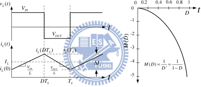
Fig. 6. Steady-state inductor voltage and current waveforms, buck type switching regulator. 11 Fig. 7 The dc conversion ratio M(D)=VOUT/VIN of buck converter. ... 11
Fig. 8. The schematic of a boost type switching regulator. ... 12
Fig. 9. Steady-state inductor voltage and current waveforms, boost type switching regulator. ... 13
Fig. 10. The dc conversion ratio M(D)=VOUT/VIN of boost converter. ... 13
Fig. 11. The schematic of a buck-boost type switching regulator. ... 14
Fig. 12. Steady-state inductor voltage and current waveforms, buck-boost type switching regulator. ... 14
Fig. 13. The dc conversion ratio M(D) of buck-boost converter. ... 14
Fig. 14. Diagram of current-mode boost converter. ... 16
Fig. 15 (a) Equivalent circuits of the first subinterval in CCM. (b) Equivalent circuits of the second subinterval in CCM ... 17
Fig. 16. Equivalent circuits of the third subinterval in DCM ... 18
Fig. 17. Operation waveform of boost converter in DCM. ... 18
Fig. 18. The HCC technique uses an error amplifier to enhance the regulation accuracy... 20
Fig. 19. The inductor current waveform is limited with the hysteresis window defined by the HCC technique. ... 21
Fig. 20. The small-signal model of the boost converter under the hysteretic current mode control. ... 23
Fig. 21. The influence of the RHP zero effect. (a) The variation of the load may cause a dip output voltage due to the existence of the RHP zero. (b) The relationship between dip output voltage and the ratio of the ωc and ωz(RHP). ... 26
Fig. 22. The simplified feedback system of the HCC regulator. ... 28
Fig. 24 The compensated loop gain T(s) (a) at heavy loads and (b) at light loads. ... 29
Fig. 25. The system architecture of the proposed boost converter with the proposed SDC technique.( LED Backlight Driver with the SDC Controller) ... 30
Fig. 26. A conventional boost converter ... 31
Fig. 27. (a). VDS(t)is the net voltage at FX. (b). iL(t) is the inductor current. (c). iD(t) is the current pass through the diode. (d). iC(t) is the output capacitor current. (e). VC(t) is the voltage between VOUT and ground. ... 31
Fig. 28. The inductor current iL(t) and the output voltage VOUT(t)waveforms of the SDC control method and the duty-increasing control. ... 33
Fig. 29. Boost converter VOUT(t) and iL(t) waveforms using in constant duty ... 40
Fig. 30. The inductor current waveform at different the off-time values. ... 41
Fig. 31. The operation of the adaptive SAR code A [7:0] by means of the gain code G[7:0]. . 42
Fig. 32. Recovery time during light load to heavy load: (a) The waveforms controlled by the PWM technique. (b) The waveforms controlled only by the new HCC technique. ... 44
Fig. 33. (a) The reduction of drop voltage and transient response are achieved by the AHW controller. (b) The reduction of drop voltage and transient response are achieved by the VTE controller. ... 45
Fig. 34. A constant-transconductance bias circuit having wide-swing cascode current. ... 48
Fig. 35. The structure of the SAR-controlled modulator. ... 49
Fig. 36. The up-down 8-bit counter. ... 50
Fig. 37. Simulation result of the up-down 8-bit counter. ... 50
Fig. 38. The 8-bit SAR gain code generator. ... 51
Fig. 39 The over-control logic circuit. ... 52
Fig. 40. The schematic of the adaptive off-time circuit and the corresponding capacitor according to each bit of the SAR code A[7:0]. ... 54
Fig. 41. Schematic of the P-Compensator. ... 54
Fig. 42. Schematic of different P-Compensator input stages. (a) Voltage follower. (b) Folded voltage follower. (c) Folded flipped voltage follower. ... 56
Fig. 46. The structure of the VTE controller. ... 59
Fig. 47. The simulation waveforms of the high speed current comparator. ... 60
Fig. 48. The theoretical (a) and simulation (b) waveforms. ... 61
Fig. 49. The structure of the AHW modulator circuit ... 62
Fig. 50. The load regulation simulation results for boost converter in different time ratios (m). ... 64
Fig. 51. The voltage drop calculation results for boost converter by comparing duty-increasing and SDC methods. ... 65
Fig. 52. The simulation and calculation results of output voltage drop value during first time period from heavy load to light load. (a) Without RESR. (b) With RESR. ... 66
Fig. 53. The total dip values of output voltage (VOUT) without RESR. ... 66
Fig. 54. The output voltage (VOUT) and inductor current (IL) waveforms. ... 67
Fig. 55. The output voltage and inductor current waveforms for boost convert when the load changed from 50mA to 250mA. ... 67
Table Captions
Table 1. Comparative table of power supply circuits. ... 7
Table 2. Comparative table of these two type control methods for boost converter. ... 37
Table 3. The linearity between ideal and actual transconductance. ... 57
Table 4. The specifications of the error amplifier ... 58
Table 5. The design specification ... 68
Chapter 1
Introduction
1.1
Background and Review
Recently the high efficiency, compact system size, and minimal components are increasingly important for today’s portable applications. For example, the function of the multimedia in mobile phone is stronger. In particular, the video and audio performances attracted more attention. Due to the demand of decent display, the light emission diode (LED) backlight becomes more popular in today’s green power mainstream.
In addition, LED does not contain infrared and ultraviolet rays in its optical spectrum. That is, it only generates minimal heat and harmful radiation making it environmentally friendly. As depicted in Fig. 1, LED lighting systems can be used on large billboards, traffic lights, streetlamps, backlighting devices [1-4], and other similar applications. Furthermore, it is very convenient to control the brightness that depends on the current flowing through LEDs. Recently, automotive electric devices with LED displays have become very popular. Thus, a high efficiency and accuracy LED driving circuit is needed in order to get an accurate control on LED brightness. Generally speaking, one of characteristics that may affect image quality is mainly determined by the backlight uniformity. Therefore, the boost converter is widely utilized for LED.
To make the power supply circuits with small size, high efficiency and better dynamic responses further, integrating some external components in chip to provide a sizable reduction in supply circuit; operate in different controlled modes with relative load current ranges and enable some machines for specific conditions are analyzed in later chapter .
Fig. 1. Application of LED lighting systems.
1.2
Classification of Voltage Regulator
General power supply circuits used in portable applications can be classified into three technologies: linear regulators, switched capacitor circuits, and switching regulators. In the following subsections, these technologies are briefly introduced and described. Finally, a brief comparison will be given about three types of voltage regulators. The comparisons included circuit complexity, cost, efficiency, load ability and so on.
1.2.1
Linear Regulators
Fig. 2 shows the schematic of a linear regulator with a pass transistor operates M1 used
power MOSFET with equivalent resistor (RDS)) between the input supply voltage and the regulated output voltage. An error amplifier controls the gate voltage of the pass resistance with respect to a reference voltage. With the error amplifier, it could adopt output voltage information form resistive feedback network (VFB) then compare to reference voltage (VREF). After error amplifier operation, it could immediately adjust input and output difference then control the gate of power MOSFET to supply load current.
Loa
d
Fig. 2. The schematic of a linear regulator.
The features of linear regulator are described as follows. Firstly, the linear regulator whole circuit is simple and compact, so the die size is smaller than other voltage regulators. And secondly, linear regulator is easy to use, instead of using inductor to transfer energy, the linear regulator just adding two capacitors at input and output pin respectively. As a result, it not only can reduces Printed-circuit board (PCB) area but also cost down. Thirdly, linear regulator only uses resistive feedback network and error amplifier output analogy signal to control power MOSFET, it doesn’t use any switching base circuits. So this kind of regulator has no Electro Magnetic Interference (EMI) and no output ripple, there are very suit for audio, analog and RF circuit applications.
But since the output current must pass through the series transistor which consumes the dropout voltage between the output and input voltages, the efficiency is low for large voltage difference between input and output voltages. The efficiency that depends on the difference of input and output voltages is given by (1):
(
)
Efficiency OUT LOAD OUT
OUT LOAD IN OUT LOAD IN
V I V
V I V V I V
⋅
= ≅
⋅ + − ⋅ (1)
1.2.2
Switched Capacitor Circuits
The switched capacitor circuit, also known as charge pumps, is usually used to obtain a dc voltage higher or lower than the supply voltage or opposite in polarity to the supply voltage in low power applications. Charge pump circuits use capacitors as energy storage devices. The capacitors are switched in such a way that the desired voltage conversion occurs.
The basic structure of two-phase charge pump regulator is shown in Fig. 3. Power stage consists of capacitors (C1 C2) and switches (S1 S2 S3 S4). Detailed operation is described as follows. The switches S1 and S2 turn on and the switches S3 and S4. turn off during the first interval of the switching period, charging capacitor CS to the input voltage level (VIN). During the second interval of the switching period, the switches S1 and S2 turn off and the switches S3 and S4. turn on, the voltage that across capacitor CS is placed in series with the input to
generate an output voltage that is twice the input voltage.
The most straightforward method is to use a control circuit and an error amplifier. The error amplifier senses the output voltage variations via the feedback resistors. The control circuit fed from the error amplifier controls switches S1 ~ S4 to regulate output voltage to a stable value through a voltage control oscillator.
Fig. 3. The schematic of a switched capacitor voltage doubler.
The features of charge pump are described as follows. Firstly, the circuit complexity of charge pump is between linear regulator and switching regulator, which is more compact than switching regulator but more complicated than switching regulator. Secondly, due to digital rail-to-rail switching clock control, the charge pump suffers from EMI and output noise problems. But this problem doesn’t heavier than switching regulator because of lower operation frequency. Finally, the load ability of charge pump is weak because the ability depends on the output capacitor C2 and switching frequency. That is to say, the larger output capacitor causes the powerful load ability. Because of light load ability typically, the charge pump is very suit for displaying applications, such as driving the gate of MOSFET to on or off.
1.2.3
Switching regulators
Switching regulators are widely used in power supply design, because it has high efficiency and power handing capability. The basic structure of boost type voltage mode switching regulator is shown in Fig. 4. The power stage of switching regulator consists of a
couple of complementary power MOSFET (MP MN), passive storage elements inductor (L) and capacitor (CO) and resistive feedback network (R1 R2). Detailed operation is described as follows; the resistors R1 and R2 sensing the variation of output voltage as the feedback signal (VFB), the error amplifier receives the voltage variation information then brings the error signal (VC). The comparator’s inputs receive the error signal from error amplifier and the ramp signal (VRAMP) from ramp generator, then compares the quantity between the error signal and the ramp signal to decide the duty cycle. After generating the control signal, the PWM generator control the detail timing to avoid short through current. At last, the purposes of gate drivers are driving huge complementary power MOSFET. At the first subinterval, lower power MOSFET (MN) turns on and upper power MOSFET (MP) turns off then input voltage source charge the inductor. At the second subinterval, lower power MOSFET (MN) turns off and upper power MOSFET (MP) turns on then the inductor will discharge to the capacitor and load. By the above-mentioned, the switching regulator adjusts the output voltage error and regulates to correct voltage.
on/off two power transistors M1 and M2, alternately. These current pulses are then converted
to continuous or discontinuous current by means of an inductive and capacitive filter.
The features of switching regulator are described as follows. Firstly, due to the storage components such as inductor and capacitor, the switching regulator can operate in three kinds of type including buck, boost and buck-boost mode. But the more external components cause the bigger PCB size and cost. Secondly, because of switching based circuits, it suffers from EMI and noise problems critically, it will take circuit layout into consideration to avoid EMI and noise problems.The most advantage of switching regulators over the linear regulators is the higher efficiency because the output pass transistors are operated as switches. When the output pass transistor is operated in the cutoff region, it dissipates no power. When the output pass transistor is operated in triode region, it is nearly a short circuit with little voltage drop across it, and it dissipates little power. In this manner, almost all power from input supply voltage is transferred to load, and high power efficiency can be achieved typically in the range from 80% to 90%, relatively independent of input to output voltage differences.
1.2.4
Comparison
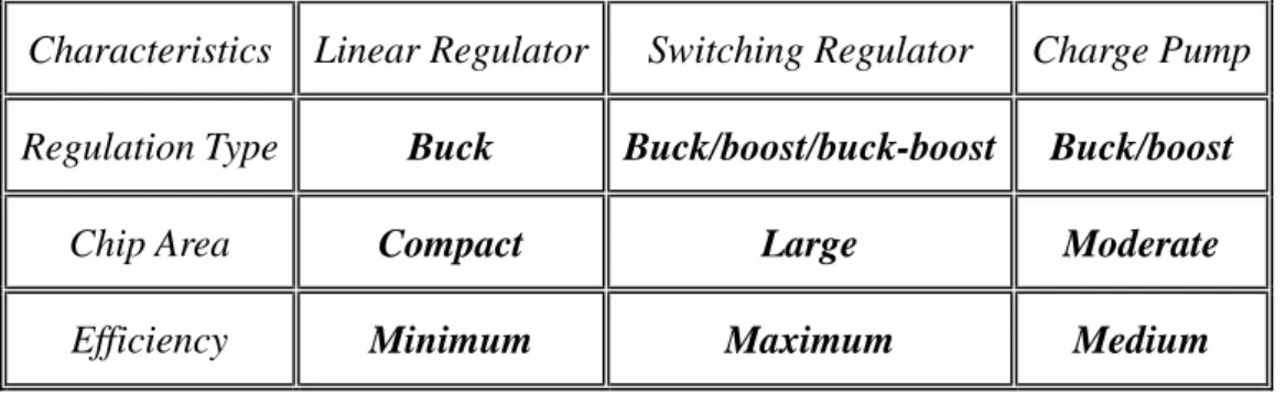
A comparison table of power supply is listed in Table 1. From Table 1, we can conclude that switching regulators are best choices for power supplies driven portable application because of their high efficiency and large power handling capability.
Table 1. Comparative table of power supply circuits.
Characteristics Linear Regulator Switching Regulator Charge Pump Regulation Type Buck Buck/boost/buck-boost Buck/boost
Chip Area Compact Large Moderate
1.3
Thesis Organization
The LED backlight driver, which is widely composed of boost converters, must demands the requirements of fast-transient, high-stability, power-efficient, and space-minimized to handle large instant load variation without sacrificing the image quality and increasing the motion blur effects. Unfortunately, unlike the design of buck converters, the transient response of the boost converter is limited by the existence of aright-half-plane (RHP) zeroin the continuous conduction mode (CCM) since the RHP zero remains the same in the design of voltage-mode or current-mode PWM and the HCC technique [5]. In conventional boost converter design, the discontinuous conduction mode (DCM) is widely used in order to get a simple compensation since the RHP zero appears at high frequency in DCM operation. But, the slow response can’t meet the requirement of the LED backlight. Thus, the better solution is to speed the transient response without being affected by RHP zero.[11-16]
EMI/Noise Minimum Maximum Medium
Load ability Medium Maximum Minimum
Complexity Simplest Complicated Medium
Chapter 2
Basic concepts of Switching Regulators
The basic topology and modulation technology of switching regulators will be introduced in this section. In the chapter 2.1, the topologies and principle of basic switching regulator topologies will be introduced. In section 2.2, we will review some modulation technologies that were used in switching regulators. In section 2.3, analysis of current mode boost switching regulator and its small signal modeling. The closed-loop with the PI compensation is also introduced in this section.2.1 The topologies and principles of basic
switching regulators
In this section some basic topology and modulation technology of switching regulators will be introduced. Following are three basic switching regulators as shown in Fig. 5 to Fig. 7 which are the buck, boost, and buck-boost converter respectively. They consist of storage element, such as an inductor (L) and a output capacitor (CO) to store and transfer energy cycle
by cycle to regulate the output voltage. The power MOSFET (M1) is controlled by the control
signal and the duty ratio is depend on the difference between the reference voltage and feedback signal from output voltage.
2.1.1
Buck converter
The fundamental operations of the three kinds of regulator are described as follow. In Fig. 5 it shows the basic structure of a buck converter. The buck converter can generate output voltage smaller than its’ input voltage. Due to the property of conversion ratio it is also called a step down converter.
Assume the magnitude of the switching ripple is much smaller than the dc component. Therefore, the output voltage VOUT( )t is well approximated by its dc component VOUT. This approximation is known as the small-ripple approximation. The steady-state inductor voltage and current waveforms are given in Fig. 6. According to the principle of inductor volt-second balance (the net change in inductor current over one switching period is zero), given the defining relation of an inductor:
0 1 ( ) (0) ( ) S T L S L L i T i v t dt L − =
∫
(2)In steady-state, the initial and final values of the inductor current are equal, and hence the left-hand side of Eq. (2) is zero. Therefore, in steady-state the integral of the inductor voltage
must be zero. ( 0 ( ) 0 S T L v t dt =
∫
). Dividing both sides of Eq. (2) by the switching period TS:0 1 0 ( ) S T L L S v t dt v T =
∫
=< > (3) L v< > is recognized as the average value, or dc component, of v tL( ). In Fig. 6 the area under the v tL( ) curve during time period TS :
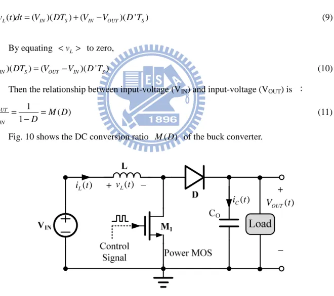
0 ( ) ( )( ) ( )( ' ) S T L IN OUT S OUT S v t dt = V −V DT + −V D T
∫
(4) By equating <vL > to zero, (VIN −VOUT)(DTS)=(VOUT)(D T' S) (5) Then the relationship between input-voltage (VIN) and input-voltage (VOUT) is :( ) OUT IN V D M D V = = (6)
( ) L v t ( ) L i t ( ) C i t ( ) OUT V t
Fig. 5 The schematic of a buck type switching regulator.
t
L I ∆ L I ( ) L S i DTt
( ) L v t IN OUT V −V OUT V − ( ) L i t S DT TS (0) L i VIN VOUT L − VOUT L − ( ) L S i Tt
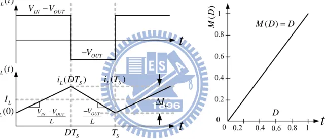
( ) M D 0 0.2 0.4 0.6 0.8 1 D 0 0.2 0.4 0.6 0.8 1 ( ) M D =DFig. 6. Steady-state inductor voltage and current waveforms, buck type switching regulator.
Fig. 7 The dc conversion ratio M(D)=VOUT/VIN of buck converter.
2.1.2
Boost converter
In Fig. 8 it shows the basic structure of a boost converter. The boost converter can generate output voltage higher than its’ input voltage. Due to the property of conversion ratio it is also called a step up converter.
The steady-state inductor voltage and current waveforms are given in Fig. 9. Like above buck converter has been introduced, and by using the principle of inductor volt-second balance. In steady-state, the initial and final values of the inductor current for boost converter
are equal, and hence the left-hand side of Eq. (7) is zero. 0 1 ( ) (0) ( ) 0 S T L S L L i T i v t dt L − =
∫
= (7)Dividing both sides of Eq. (7) by the switching period TS:
0 1 0 ( ) S T L L S v t dt v T =
∫
=< > (8) L v< > is recognized as the average value, or dc component, of v tL( ). In Fig. 9 the area under the v tL( ) curve during time period TS :
0 ( ) ( )( ) ( )( ' ) S T L IN S IN OUT S v t dt = V DT + V −V D T
∫
(9) By equating <vL > to zero, (VIN)(DTS)=(VOUT −VIN)(D T' S) (10) Then the relationship between input-voltage (VIN) and input-voltage (VOUT) is :1 ( ) 1 OUT IN V M D V = −D = (11)
Fig. 10 shows the DC conversion ratio M D( ) of the buck converter.
( ) L v t ( ) L i t ( ) C i t ( ) OUT V t
t
L I ∆ L I ( ) L S i DTt
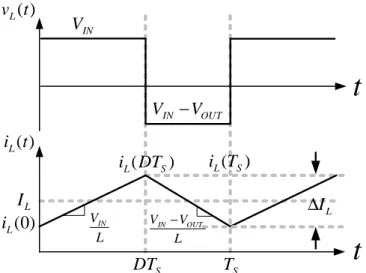
( ) L v t IN OUT V −V IN V ( ) L i t S DT TS (0) L i VIN L IN OUT V V L − ( ) L S i Tt
( ) M D 0 1 D 0 0.2 0.4 0.6 0.8 1 1 1 ( ) ' 1 M D D D = = − 2 3 4 5Fig. 9. Steady-state inductor voltage and current waveforms, boost type switching regulator.
Fig. 10. The dc conversion ratio M(D)=VOUT/VIN of boost converter.
2.1.3
Buck-Boost converter
Fig. 11 shows the basic structure of a buck-boost converter. The buck-boost converter has both the characteristic of buck and boost converter. Thus, it is also called a step up-down converter. The steady-state inductor voltage and current waveforms are given in Fig. 12. As before, we use the principle of inductor volt-second balance to find the relationship between input-voltage (VIN) and input-voltage (VOUT) in steady-state :
0 ( ) ( )( ) ( )( ' ) S T L IN S OUT S v t dt = V DT + V D T
∫
(12) (VIN)(DTS)= −( VOUT)(D T' S) (13) Then the relationship between input-voltage (VIN) and input-voltage (VOUT) is :( ) 1 OUT IN V D M D V D − = = − (14) Fig. 13 shows the DC conversion ratio M D( ) of the buck converter.
( ) L v t ( ) L i t
Fig. 11. The schematic of a buck-boost type switching regulator.
t
L I ∆ L I ( ) L S i DTt
( ) L v t OUT V IN V ( ) L i t S DT TS (0) L i VIN L OUT V L ( ) L S i Tt
( ) M D D 1 1 ( ) ' 1 M D D D = = −Fig. 12. Steady-state inductor voltage and current waveforms, buck-boost type switching regulator.
Fig. 13. The dc conversion ratio M(D) of buck-boost converter.
2.2 Analysis of current-mode Boost Switching
regulator
Current-mode control DC-DC converter is already surpassed 30 years history until now.
Current-mode control in power supplies is difficult to be analyzed because of its multi-loop
architecture. In the current-mode control technique, the output voltage of the converter is not
The current feedback loop results in some unique advantages compared to the voltage-mode controller. These advantages contain: line regulation is improved, the compensation network is simple, dynamic performance traits change little between CCM and DCM operation, and current limiting mechanism is also built into the architecture. In many cases the current mode control technique can enhance performance of the switching regulators.
2.2.1 The Operation Theorem of Current Mode Control
The block diagram of current mode boost converter is shown in Fig. 14. There are two operation modes for switching converter, which are voltage mode and current mode.
In voltage mode controlling, the converter only uses a voltage feedback loop to regulate the output voltage. The duty ratio of pulse-width modulation is produced by output signal of error amplifier and the original ramp signal.
In current mode controlling, it includes both voltage and current loop. The advantage of current mode is its simpler dynamics and wide-bandwidth. The inductor and capacitor of power stage offer only one low frequency pole. Otherwise, current mode control should be used of the current sensing information during the normal operation to obtain simpler dynamics.
In Fig. 14 the PWM signal is generated by clock generator with a pulse of small duty ratio. The output of the SR latch should be set to high when the output signal of clock generator is high. In this state, the power MOSFET (M1) is turned on and diode off. The
inductor current increases with a positive slope depend on the input voltage and the value of inductor. The artificial ramp is added to the current sensing signal to avoid unstable problem when duty ratio is larger than 0.5. The error signal and the sum of ramp and current sensing are compared by the analog comparator. When the sum of ramp and current sensing is larger than error signal (V ), the output of comparator is high to reset the SR latch and turn off the
power MOSFET. Therefore, the duty cycle of power MOSFET (M1) is controlled by not only
feedback voltage but also inductor current.
Fig. 14. Diagram of current-mode boost converter.
2.2.2 Continuous Conduction Mode (CCM)
In the CCM operation the inductor current has a minimum level above zero and operates continuously. Therefore, there are only two subintervals for switching converter in CCM operation. The two equivalent circuits of first and second subintervals are as shown in Fig. 15.
Fig. 15 (a) shows the first subinterval operation in CCM. When converter operating in first subinterval the low side NMOS turns on and inductor current increasing. During this subinterval the inductor voltage and output capacitor current can be derived as equation (15) and (16). L ( ) L in di v t L V dt = = (1)
Fig. 15 (b) shows the second subinterval operation in CCM. When converter operating in first subinterval the high side PMOS turns on and inductor current delivering to output. During this subinterval the inductor voltage and capacitor current can be derived as equation (17) and (18). ( ) L L in out di v t L V V dt = = − (17) ( ) O O C out C O L L dv V i t C i dt R = = − (18) ( ) L V t + − i tC( ) V IN VOUT L CO RL ( ) L V t + − i tC( ) + _ (a) (b)
Fig. 15 (a) Equivalent circuits of the first subinterval in CCM. (b) Equivalent circuits of the second subinterval in CCM
By capacitor charge balance, the steady-state current in the switching converter can be calculated as shown in equation (19).
(
1)
0 , 2' '
out out out in
S L S L L L L L V V V V DT i D T i R R D R D R − ⋅ + − − ⋅ = = = (19)
The inductor current in equation (18) is equal to the input current of converter. Its’ magnitude is greater than the load current. By combining the equation (15) and (16) the inductor current ripple and output voltage ripple can be calculated as equation (20) and (21) respectively: 2 in L S V i DT L ∆ = ⋅ (20) 2 O C S L O V v DT R C ∆ = ⋅ (21)
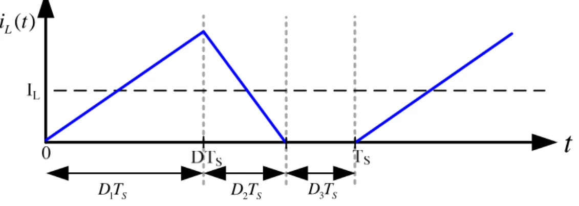
2.2.3 Discontinuous Conduction Mode (DCM)
In the DCM operation the inductor current has a minimum level equal to zero. Therefore, the operation region will be defined as three subintervals for switching converter in DCM operation. However, the first and second subinterval are as the same as CCM operation. Thus, the equivalent circuit in Fig. 16 has just shows the third subinterval. In the third subinterval the power MOSFET and diode are both turn off, the energy store in output capacitor to discharge to load. Owing to the three subintervals in the DCM operation, one switching cycle has divided into three parts,D T1 S , D T2 S and D T3 S . The operation waveform of boost converter is shown in Fig. 17.
( )
L
V t
+
−
i t
C( )
Fig. 16. Equivalent circuits of the third subinterval in DCM
( )
Li t
t
1 S D T D T2 S D T3 Ssubinterval are shown in equation (22) and (23). 0 L v = (2) , 0 out C L L V i i R = − = (3)
By inductor voltage second balance, equation (24) can be derived. The conversion ratio is relative to the duty ratio of the first and second subintervals.
(
)
1 2 1 2 3 2 0 0 , out in s in out s S in V D D V D T V V D T D T V D + ⋅ + − ⋅ + ⋅ = = (4)By capacitor charge balance, the steady-state current in the switching converter can be calculated as shown in equation (25).
1 2 1 2 1 1 2 2 in in S out S S L S V V D D T V I D T D T R T L L = = ⋅ ⋅ = (25)
By replacing equation (25) into (24) the output voltage can be obtained as:
2 4 1 1 2 , 2 out in L S D V K L where K V R T + + ⋅ = = (26)
As mention in 2.2.2 the conversion ratio in CCM operation only depends on input voltage and duty cycle. However, in DCM operation the voltage conversion ratio depends on the inductor, load resistance, switching frequency and input voltage.
2.3 The Small Signal Modeling of the HCC Boost
Converter
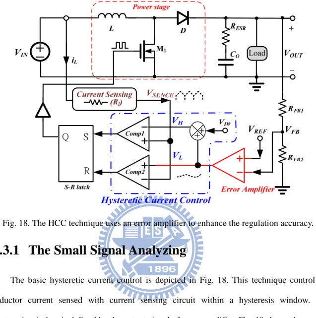
Owing to low power consumption requirement, the hysteretic current control (HCC) technique is selected as the modulation method for LED backlight. A simple structure is illustrated in Fig. 18.
Fig. 18. The HCC technique uses an error amplifier to enhance the regulation accuracy.
2.3.1 The Small Signal Analyzing
The basic hysteretic current control is depicted in Fig. 18. This technique control the inductor current sensed with current sensing circuit within a hysteresis window. The hysteresis window is defined by the output signal of error amplifier. Fig. 19 shows the control behavior of inductor current. The inductor current rises until it reaches the upper band of hysteresis window during ton period when the high-side MOSFET turns on [7]. When the low-side MOSFET turns on during toff period, the inductor current falls to reach the lower band of hysteresis window This HCC technique is simple and has fast dynamic characteristics due to its unlimited on-time value, but it is poor on electromagnetic interference (EMI) issue.
s on off
t
=
t
+
t
(27)s
k t
⋅
k t⋅ +( s ton)(
k+ ⋅1)
tsFig. 19. The inductor current waveform is limited with the hysteresis window defined by the HCC technique.
(
)
,
on off in o inLH
LH
t
t
v
v
v
=
=
−
(28)The peak inductor current, ip, can be expressed as (29) and the average inductor current
<iL>.
(
)
2
2
in o in p L on L offv
v
v
i
i
t
i
t
L
L
+
=
+
=
+
(29)Now, let’s consider the small signal analysis. The value of each variable can be written as the summation of two components the DC term and its AC perturbation. The duty cycle, d, and its complementary value, d’ are shown in (30) and (31).
ˆ
s s s
t
= +
T
t
,t
on=
T
on+
t
ˆ
on, andt
off=
T
off+
t
ˆ
off=
d t
'
s (30)ˆ
d
= +
D
d
andd
'= − =
1
d
D
'−
d
ˆ
(31) Hence, (27) and (28) can be re-written as (32) and (33), respectively.(
ˆ
) (
ˆ
)
(
ˆ
)
s s on on off off
(
)
ˆ
ˆ
ˆ
off off o o in inLH
T
t
V
v
V
v
+
=
+ −
−
(33)By keeping the first-order ac terms, (30) and (29) can be re-written as (34) and (35), respectively. The small-signal equations can be derived in (34).
ˆ
ˆ
ˆ
s on offt
=
t
+
t
,ˆ
ˆ
onˆ
s st
Dt
d
T
−
=
, and(
)
2(
)
ˆ
ˆ
ˆ
off o in o inLH
t
v
v
V
V
= −
−
−
(34)(
)
(
ˆ ˆ)
2 ˆ ˆ ˆ ˆ ˆ ˆ and 2 in on on in on on p L in p L in in V t T v L T t i i v i i V V L + = − − = + (35)Therefore, the small-signal duty cycle is derived as (36).
' '
2
1
ˆ
(
ˆ
ˆ
)
ˆ
ˆ
P L in o o oD D
D
d
i
i
v
v
H
V
V
⋅ ⋅
=
−
−
+
(36)By using the DC equivalent equations, (36) can be simplified as (37).
(
)
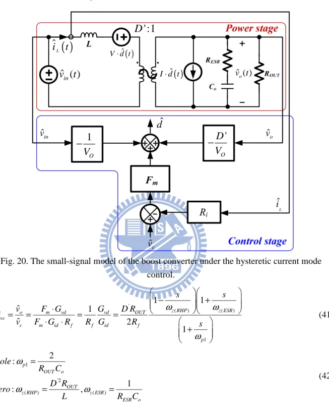
1 ' ˆ ˆ ˆ ˆ ˆ m C i L in o O O D d F v R i v v V V = − ⋅ − ⋅ + ⋅ (37) 2 ' m i DD where F HR = (38)As a result, the small-signal model of the hysteretic current mode boost converter is illustrated in Fig. 20. The control-to-output transfer function is shown in (39). ROUT is the
output impedance. Ri is the current sensing equivalent resistance. RESR is the equivalent series
resistance of output capacitor, Co.
ˆ ' ˆ 1 o m vd vc c vd m id i O v F G G D v G F G R V ⋅ = = − ⋅ + ⋅ ⋅ (39)
(
)
'2 ' 1 1 ˆ ˆ ESR o o o vd L s sR C v V D R G LC L − + = = ⋅ and '2 1 ˆ 2 2 ˆ o o L id RC s V i G LC + ⋅ = = ⋅ (40)Because of that Fm⋅Gid⋅Rf >> − ⋅1 k Gr vd, (39) can be simplified as (41) ˆc v ˆ L i ˆo v
ˆ
d
ˆin v( )
Li
t
ɵ
( )
ˆ V d t⋅' :1
D
( )
ˆ I d t⋅ˆ ( )
inv t
v tˆ ( )o1
OV
−
'
OD
V
−
Fig. 20. The small-signal model of the boost converter under the hysteretic current mode control. ' ( ) ( ) 1 1 1 ˆ 1 ˆ 2 1 z RHP z ESR o m vd vd OUT vc c m id f f id f p s s v F G G D R G v F G R R G R s ω ω ω − + ⋅ = = = = ⋅ ⋅ + (41) 1 '2 ( ) ( ) 2 : 1 : , p OUT o OUT z RHP z ESR ESR o pole R C D R zero L R C ω ω ω = = = (42)
It is obvious to find that there are one dominant pole (ωp1) and two zeros (one RHP zero,
ωz(RHP), and one LHP zero, ωz(ESR)). The frequency response of the HCC technique is similar
to that of the current-mode PWM technique. Hence, the proportional-integral (PI) compensation is enough to choice. The PI compensator has a transfer function as shown in (43). ω is used to cancel the effect of power stage pole (ω ). And ω replaces ω toforms
the new dominant pole to determine the system bandwidth. The role of ωpc2 is used to
decrease the high-frequency gain due to the existence of ωz(RHP).
1 0 1 2 1 1 1 zc c c pc pc s G G s s ω ω ω + = + + (43)
Comparing to conventional current-mode PWM controller, the HCC technique doesn’t need slope compensation to reduce sub-harmonic oscillation when perturbation happened. In other words, the compensation in the HCC technique is much simpler than the current-mode PWM technique. However, the RHP zero which seriously affects the system stability still exists in both techniques
2.3.2 Right Half Plane (RHP) zero
RHP zeros are a property of a special class of active circuits which have a tendency to respond initially in the wrong direction when given a changed input. Eventually, the output will move in the direction commanded by the input. How fast it starts moving in the right direction is determined by the frequency location of the RHP zero. Boost and flyback converters are very popular circuits in use in the industry today, and both have RHP zero characteristics when operating in continuous conduction mode.
The cause of the RHP zero for these converters is the same and intuitive. The output capacitor of the converter is charged by the inductor current, but only when the power switch is turned off. An initial increase in duty cycle of the power switch increases the current in the inductor within one cycle, but the net charge to the output capacitor (product of the inductor
This can be confusing for a controller that is monitoring the output voltage to make control decisions. There is no alternative but to wait and see where the long-term trend is before adjusting the duty cycle.
2.3.3 The effect of the RHP zero
When heavy loads happened, the RHP zero effect becomes worse to affect the system stability as illustrated in Fig. 21(a) and (41). A reasonable design limitation on the crossover frequency, ωc, should be below 1/10 of the switching frequency. When the designed crossover
frequency is higher, more issues with noise will arise. In addition, the designed crossover frequency is also considered the influence of RHP zero. To reduce this effect it should be smaller than the 10~20% RHP zero, which is the RHP zero at heavy loads, as the illustrated in Fig. 21(a). When the crossover frequency is far away the RHP zero, the output voltage (Vo,)
has no dip voltage in case of load current variation. That is, the RHP zero has little effect on the undershoot output voltage. However, because of small bandwidth the transient response is too slow and thus the output voltage has a large dip voltage. Although, a large bandwidth can shorten the transient response and get a small dip voltage. An increasing crossover frequency may have a large dip voltage due to the existence of the RHP zero. In order to get a smallest dip output voltage. It need to confer the relationship between ωc and ωz(RHP) and to. There
exists an optimum ratio between the ωc and ωz(RHP), which is labeled as ΔVo(optimum) at point
C. But the phase margin at this optimum dip voltage is not good enough due to ωz(ESR) and one
high-frequency pole from the compensator. Therefore, the system bandwidth needs to be extended to compensate the dip voltage due to the RHP zero and not be limited by 10~20% RHP zero. The designed value is set at point B, which is about 30% of the RHP zero.
2 ( )
(1
)
out Z RHPD
R
L
ω
=
−
⋅
(a)D
ip
o
u
tp
u
t
v
o
lt
a
g
e
(
m
V
)
(b)Fig. 21. The influence of the RHP zero effect. (a) The variation of the load may cause a dip output voltage due to the existence of the RHP zero. (b) The relationship between dip output voltage and the ratio of the ωc and ωz(RHP).
is the compensation transfer function that is composed of an error amplifier and a PI compensator.
( ) ( ) c( ) vc( )
T s =H s G s G⋅ ⋅ s (44)
Fig. 23 shows the PI compensator which contributes one low-frequency pole-zero pair, (ωpc1, ωzc1), and one high-frequency pole, ωpc2 (to avoid switching noise). The transfer
function from the feedback signal (VFB)to the error amplifier output (VC) is shown as equation
(45). 1 1 1 1 1 1 (1 ) 1 [ / /( )] , (1 ) C C Z m O Z m O O Z FB C C O V s C R g R R g R if R R V sC s C R + ⋅ ⋅ = ⋅ + = ⋅ ⋅ >> + ⋅ ⋅ (45)
Where gm and RO are the transconductance and the output resistance of the error
amplifier, respectively. Therefore, the pole and zero contributed by the compensation network are as follow. 1 1 2 1 1 1 2 1 1 1 1 : zc , : pc , pc C Z C O C Z zero pole C R C R C R
ω
=ω
=ω
= ⋅ ⋅ ⋅ (5)To make sure the stability of the system, in this kind of compensation technique the pole which is used to replace the system pole and becomes the dominate pole. Furthermore, the unit gain frequency of the loop is determined by the compensation resistance. Thus, the frequency response of the system can be improved by choosing an optimal compensation resistance.
ˆ ( )
ov s
ˆ ( )
cv s
ˆ ( )
ev s
Fig. 22. The simplified feedback system of the HCC regulator. R1 R2 VREF RO RZ1 CC1 VOUT VFB VC Error Amplifier Compensation Network CC2
g
mFig. 23. The PI compensator of HCC dc-dc converter
The loop gain T(s) can be illustrated in Fig. 24 at light and heavy loads. Using the compensation zero (fzc1) in the PI compensator to cancel the pole of power stage of the
converter (ωp1), then the system bandwidth will be extended. The RHP zero ωz(RHP) will
decrease at heavy loads, which is represented by a solid dash line in Fig. 24(a). According to Fig. 24(b), the ratio of ωc and ωz(RHP) has an optimum value when the dip output voltage is the
major concern. That is the compensation zero ωzc1 is decided at heavy loads.The bandwidth
becomes worse due to the decrease of ωp1 at light loads. As the reason explained before, the
1 zc f fpc2 1 pc f 1 p f 1 zc f fpc2 1 pc f 1 p f 80dB 60dB 40dB 20dB 0dB -20dB 1K 10K 100K 1M 10M 100 Gain -40dB 1 p f 1 pc f 1 zc f fpc2
@Light Load
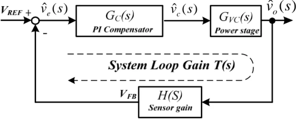
Frequency (Hz) System Loop T(s) PI Compensator Gc(s) Modulator Gvc(s)Feedback Sensing Gain H(s)
fz(RHP) fz(ESR) ω=2πf 0 -45 -90 -135 -180 -225 1K 10K 100K 1M 10M 100 θ -270 1 p f 1 pc f 1 zc f fpc2 Frequency (Hz) fz(RHP) fz(ESR) (a) (b)
Chapter 3
The Proposed RHP Zero Alleviating
Technique in the SDC Boost Converter
D ea d -t im e D ri ve r C O M P L
Fig. 25. The system architecture of the proposed boost converter with the proposed SDC technique.(LED Backlight Driver with the SDC Controller)
The proposed SDC architecture is shown in Fig. 25. The circuit implementation with a hysteresis window formed by the value of VCT, which is generated by the voltage divider from
the bandgap circuit, allows the output ripple to be limited within this hysteresis window and adjust the trailing and leading edges for fast transient response. In case of heavy load condition, the on-time period suddenly increases while the off-time period decreases. The energy, delivered to the output decreases in the beginning, seriously causes the output has a large voltage drop. After the inductor current increases to a higher value, the output voltage can be pulled back to its regulated value. In other words, the RHP zero effect induces a large
3.1
The Constant duty Analysis for Boost
converter
( ) L i tL
+
+
−
−
VDS( )t ( ) D i t ( ) C i t Load I C IN V+
−
( ) OUT V t+
−
C( ) V t 1 MFig. 26. A conventional boost converter
( ) DS V t
t
t
L I ∆ ( ) L i t L I 1 I 2 I ( ) D i tt
1 I 2 I ( ) C i tt
1 Load I −I 2 Load I −I Load I ( ) C V t S DT TS DTS+TSt
_ 1 (2 1 2) L off I = I +I S DT TS DTS+TS 1 C V 2 C V _ 2 1 C ontime C C V =V −V _ 1 2 C offtime C C V =V −VFig. 27. (a). VDS(t)is the net voltage at FX. (b). iL(t) is the inductor current. (c). iD(t) is the
current pass through the diode. (d). iC(t) is the output capacitor current. (e). VC(t) is the
voltage between VOUT and ground.
The SDC method could reduce the RHP effect due to the extension of the on-time and the off-time periods during transient response. A conventional boost converter is illustrated in Fig. 26, including Fig. 26 the current and voltage waveform are shown in Fig. 27. Here we assume all switching devices and passive elements are ideal. In the other words, the voltage
across is zero when the Power NMOS (M1) and the diode are turned on. The voltage variation on the output capacitor during the on-time and off-time periods can be expressed as (47) and (48), respectively. These two equations also indicate the output voltage variation during the on-time (VC_ontime) and off-time (VC_offtime) periods.
_ Load C ontime S I V DT C = (47) _ ' _ ( L offtime Load) C offtime S I I V D T C − = (48)
Where ILoad is the load current, and IL offtime_ is the current value pass to output
through diode during off-time periods. The total voltage drop on the capacitor can be shown as (49) by subtracting equation (47) and (48).
_ _
C C ontime C offtime outdrop
V V V V
∆ = − + = − (49)
Section 3.1.1 and 3.1.2 will compare two different methodology used in boost converter when the load step happened. They are conventional duty-increasing method and constant duty method, respectively.
3.1.1 Type 1:
:
:Duty Increasing Methodology
:
The output voltage VOUT(t) and inductor current iL(t) waveforms for duty increasing
boost converter is shown in Fig. 28. The output capacitor of the converter is charged by the inductor current only when the power switch is turned off. When load transient happened, an initial increase in duty cycle of the power switch increases the current in the inductor within one cycle, but the net charge to the output capacitor (product of the inductor current and off-time) is initially less. Hence, an increase in command to the system results in a large temporary droop in the output voltage.
arg ch e Q arg disch e Q 1 1 n n S D T− − 1 1 n n S D T− − 1 n S T− 1 n S T− n n S DT n n S DT n S T n S T 1 ' ' 1, 1, and n n n n n n S S D D D D T mT − − − = = = _ n 1 (2 2 3) L offtime I = I +I _ 1 2 3 'L offtimen 2( ' ') I = I +I 1 1 1 1' ' 1' n n n n on n n n S off n n n S t t D D D D T t D D D D T − − − − − + ∆ → = = + ∆ → = = − ∆ (k>1)
Fig. 28. The inductor current iL(t) and the output voltage VOUT(t)waveforms of the SDC
control method and the duty-increasing control.
For duty-increasing method the on-time will increase when load step happened at time t1,
the value of on-time, off-time and switching period will change to equation (50).
1 1 1, 1 n n n n n n on on off off S S t t t t t T mT m − − − = + ∆ = = > (50) t
∆ is the on-time increasing value at heavy-load. The duty cycle can be expressed as
1
n n
D =D − + ∆D and Dn'=Dn−1'− ∆D. Then the output voltage variation during this time period is shown as (51). 1 1 _ _ _ sin ( ) ( ) n n n n n n
Load L offtime Load C duty incre drop duty increa g on off
I I I V V t t t C − C − − − − ∆ = − = − + ∆ + (51)
_ n
L offtime
I is the off-time average inductor current value when load variation happened, and it’s equal to the half sum of I2 and I3 in (52). ∆IL is the inductor current variation before
load transient which is equal to
1 1 1 n n L IN n S I V L D T − − − ∆ = . 1 1 2 1 3 2 2 3 1 2 ( ( )) ' ' 2 n n n n n n n L L IN n S IN out out n S IN S n out n S I I I V I I D T L V V V I I D T L V T D V D T I I I L L − ∆ = − = + − − ∆ = + ∆ + = + + (52) Where the 1 n n out out V V
− − ∆ means the output voltage dc component during time period t1
and t2 , and ∆Voutn can be expressed as (53).
1 1 1 _ 1 ( ) ' n n n n n n
Load L offtime Load
out n S n S I I I V D T D T C C − − − − − ∆ = − (53) 1 _ n L offtime I
− is the off-time average inductor current value before load variation happened,
which equal the inductor current dc component at light-load. By replacing equation (52) into
_ n
L offtime
I the off-time average inductor current can be obtained as:
1 _ 1 ' [ ] 2 2 n n n n n out n S IN L offtime L n S n S V D T V I I D T D T L − − L ∆ = + − + (54)
In order to simplify the equation, we let the demand inductor current at light-load and heavy-load are IL and kIL(k >1), respectively. So (53) can be simplified to (55).
1 1 1 1 ' ( ' ) ' n n n n L L n L out n S n S D kI I D I V D T D T C C − − − − − ∆ = − 1 1 1 ' [ ] n n L n n S n S I D D kT D T C − − − = − (55)