國
立
交
通
大
學
電機學院微電子奈米科技產業研發碩士班
碩
士
論
文
以時間轉換數位為基礎之低成本溫度感測器設計
Design of a Low-Cost temperature sensor
on Time-to-digital Conversion
研 究 生:郭時明
指導教授:李鎮宜 教授
以時間轉換數位為基礎之低成本溫度感測器設計
Design of a Low-Cost temperature sensor
on Time-to-digital Conversion
研 究 生:郭時明 Student:Shyr-Ming Kuo 指導教授:李鎮宜 Advisor:Chen-Yi Lee 國 立 交 通 大 學 電機學院微電子奈米科技產業研發碩士班 碩 士 論 文 A ThesisSubmitted to College of Electrical and Computer Engineering National Chiao Tung University
in partial Fulfillment of the Requirements for the Degree of Master
in
Industrial Technology R & D Master Program on Microelectronics and Nano Sciences
October 2010
Hsinchu, Taiwan, Republic of China
以時間轉換數位為基礎之低成本溫度感測器設計
學生:郭時明 指導教授:李鎮宜 國立交通大學電機學院產業研發碩士班 摘 要 本論文研製之溫度感測器是以 CMOS 為主,由時間轉數位,內建於晶 片,且為低成本的設計。由於不依賴任何 BJT 電晶體或類比轉數位器, 所需晶片面積相對很小且耗電量亦低。其精簡的結構致使容易嵌入任 何 CMOS IC 晶片內。此溫度感測器所產生之數位碼與溫度成正比之關 係,是以時間轉數位之方式達成。此數位碼再參照對應溫度表即可用 以表示目前溫度狀態。測試晶片是以 UMC CMOS 90nm 1P9M 製程所製造, 其核心面積極小為 0.01004 平方公釐。若無經校正,有效解析度約為 ±0.14℃;若加入校正電路,則正好為 0.1℃,且線性度極佳。Design of a Low-Cost temperature sensor on
Time-to-digital Conversion
student:Shyr-Ming Kuo Advisors:Dr. Chen-Yi Lee
Industrial Technology R & D Master Program of Electrical and Computer Engineering College
National Chiao Tung University
ABSTRACT
The proposed design is a CMOS-based, time-to-digital, on-chip and lost-cost temperature sensor. Without relying on any bipolar transistor or analog-to-digital converter, the required chip area is relatively small and the power consumption is low. Its simple structure allows it to be freely embedded onto any CMOS IC chip. The sensor generates a digital code proportional to temperature by time-to-digital method. The code with a lookup table can be directly used to indicate current thermal status. The test chip fabricated in the UMC CMOS 90nm 1P9M process has a extremely small area of 0.01004mm2. The effective resolution is around ±0.14℃ without calibration and exactly 0.1℃ plus perfect linearity with calibration.
誌
謝
感謝李老師這幾年的指導與照顧,相信他的好脾氣大家都
深感認同,也相對讓學生覺得沒有特別的壓力感,在這樣無壓
迫感的環境下作研究是最愉快不過了。另外要特別感謝余建螢
學長和馬曉涵的慷慨協助,耐心教導我一些基礎的工具使用方
法,致使我能順利完成研究工作。
目
錄
中文提要 ……… I 英文提要 ……… II 誌謝 ……… III 目錄 ……… IV 表目錄 ……… VII 圖目錄 ……… VIII 符號說明 ……… XI Chapter 1 Introduction………..… 1 1.1 Motivation……….. 1 1.2 Contribution………..…. 2 1.3 Thesis organization……….... 3
Chapter 2 Overview of Related Works……….... 5
2.1 A short history of smart temperature sensor………..…… 5
2.2 Micropower CMOS temperature sensor with digital output….. 7
2.3 A switched-current/capacitor temperature sensor………..…… 8
2.4 A Low-Cost High-Accuracy CMOS Smart temperature sensor……….……… 8
2.5 A high-accuracy temperature sensor with second-order curvature correction and digital bus interface……… 9
2.6 A CMOS temperature sensor with a 3σinaccuracy of ±0.5℃ from -50℃ to 120℃……….……… 9
2.7 A Time-to-Digital-Converter-Based CMOS Smart Temperature Sensor……… 10
2.8 A summary of the related works……….…... 11
Chapter 3 Proposed Architecture and Algorithm………..… 12
3.1 Proposed Architecture……… 12
3.1.1 Design basis……….………….……… 12
3.1.3 Design concept……….…….……… 13
3.1.4 Signal flow……… 14
3.1.4.1 A simple pulse generator……….……… 17
3.1.4.2 A Time-to-Digital Converter……… 18
3.2 Algorithm……….………….……….……… 18
3.2.1 The thermal-sensitive delay line….……….……….…… 19
3.2.2 The pulse-expanding delay line……… 27
3.2.2.1 Inverter chain method……….….……… 27
3.2.2.2 Vernier Delay Chain method……… 28
Chapter 4 Circuit Design and Performance Comparison…………..… 35
4.1 Circuit Design……… 35
4.1.1 The pulse generator………….……….……….…… 35
4.1.2 The thermal-sensitive delay line………….…….….…… 36
4.1.3 The pulse-expanding delay line……… 37
4.1.4 The digital counter……… 38
4.2 Performance Comparison….……….………… 42
Chapter 5 Simulation and Measurement results……… 43
5.1 Simulation results……….……….……… 43
5.1.1 Pre-Sim……….……… 43
5.1.2 Post-Sim……… 45
5.1.3 Layout arrangement……….……….………… 47
5.1.4 Tape-Out chip……… 50
5.2 Chip Design and Measurement results….………….………… 53
5.2.1 Chip Design………..……… 53
5.2.2 Measurement results……….……… 54
5.2.3 Testing Environment……… 56
Chapter 6 Conclusion and Future Research……… 60
6.2 Future Research……….……….……… 60 References ……….……….…….…… 62 自傳 ……….………..……… XII
表
目
錄
Table 1 The common specifications of smart temperature sensors
……… 7 Table 2 A summery of the related works
……… 11 Table 3 The performances of the two temperature sensors
……… 27 Table 4 The comparison with other temperature sensors
圖
目
錄
Fig.1 The Overall structure of the smart temperature sensor
……… 2 Fig.2 The typical block diagram of the conventional smart
temperature sensor……… 5 Fig.3 The architecture of the proposed temperature sensor
……… 12 Fig.4 The Signal flow of the proposed temperature sensor
……… 14 Fig.5 The principles of the operation in the circulating loop
……… 15 Fig.6 A simple pulse generator
………..……… 17 Fig.7 A Time-to-Digital Converter
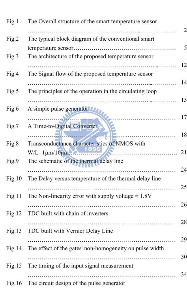
………..……… 18 Fig.8 Transconductance characteristics of NMOS with
W/L=1μm/10μm……… 21 Fig.9 The schematic of the thermal delay line
………..……… 24 Fig.10 The Delay versus temperature of the thermal delay line
……….……….……… 25 Fig.11 The Non-linearity error with supply voltage = 1.8V
……….……….……… 26 Fig.12 TDC built with chain of inverters
……….……….……… 28 Fig.13 TDC built with Vernier Delay Line
……….……….……… 29 Fig.14 The effect of the gates' non-homogeneity on pulse width
……….……….……… 30 Fig.15 The timing of the input signal measurement
……….……….……… 34 Fig.16 The circuit design of the pulse generator
……….……….……… 35 Fig.17 The circuit design of the thermal delay line
……….……….……… 36 Fig.18 The circuit design of the pulse-expanding delay line
……….……….……… 37 Fig.19 The binary counting circuit of the basic 4-bit counter
……….……….……… 39 Fig.20 The different input scheme of the basic 4-bit counter
……….……….……… 40 Fig.21 The circuit design of the J-K flip-flop
……….……….……… 41 Fig.22 The code word vs. temperature characteristics of the Pre-Sim
for the old design………….………..……… 44 Fig.23 The code word vs. temperature characteristics of the Pre-Sim
for the new design……….……….……… 45 Fig.24 The code word vs. temperature characteristics in the Post-Sim
for the old design………….………..……… 46 Fig.25 The code word vs. temperature characteristics in the Post-Sim
for the new design……….……….……… 47 Fig.26 The phenomenon of the layout arrangement
……….……….……… 49 Fig.27 The tape-out chip of the proposed temperature sensor without
calibration circuit……….………….……… 51 Fig.28 The tape-out chip of the proposed temperature sensor without
calibration circuit and I/O pad……….….……… 52 Fig.29 The layout for the new design of the proposed temperature
sensor with calibration circuit and I/O pad…….…..………… 53 Fig.30 The chip die photo and the chip design
……….………….……… 54 Fig.31 The measurement results of the tape-out chip
……….………….……… 55 Fig.32 The testing equipments and the test chip
……….………….……… 57 Fig.33 The Agilent Logic Analysis System 16902A
……….………….……… 57 Fig.34 The Agilent Logic Analysis System 16902A
……….………….……… 58 Fig.35 The Low Temperature Incubator
……….………….……… 59 Fig.36 The test chip
符 號 說 明 mm2 :mini-meter squared nm :nano (10-9) meter ± :plus or minus ℃ :degree of Celsius ns :nano (10-9) second Δ :potential gradient μ :micro (10-6 ) σ :precision
Chapter 1
Introduction
1.1 Motivation
Nowadays the growing market of portable systems demands low-cost on-chip temperature sensors. Besides, almost every essential part of IC device requires thermal monitor to prevent the device from overheating which is detrimental to electronic devices, especially for high performance IC chips.
The important applications of on-chip temperature sensors include: 1) The power consumption control in VLSI chips, such as CPU and chipsets; 2) The environment temperature monitor or control of consumer electronics.[1]
The researches on smart or integrated temperature sensors started in the mid-seventies, together with the development of the Integrated Circuit (IC) technology. In the early works on smart temperature sensor, bipolar substrate transistors are utilized to make a temperature sensor compatible to standard CMOS technology.
Recently, it is well-known that delay of a logic gate has a positive temperature coefficient if the supply voltage is large enough in comparison with threshold voltage of device [2]. This characteristic can be utilized for temperature measurement to reduce the complexity and eliminate error correction techniques. A novel work [12] presented a smart temperature sensor
using delay lines to generate pulse width which is proportional to temperature. Figure 1 is the overall structure of the smart temperature sensor. The delay line and a XOR gate will generate a pulse width proportional to temperature. This pulse will circulate and shrink in the cyclic time-to-digital converter until the pulse completely vanishes.
Fig.1 The Overall structure of the smart temperature sensor [12]
This structure has brought a new choice for small area, low complexity and low power when designing a temperature sensor. But when supply voltage is scaled down and a wide range of measured temperature is required, the practical temperature versus delay line will derive from the linear one considerably. Therefore, its implementation is limited in a small area of applications.
1.2 Contribution
The pulse-shrinking mechanism in Chen’s design [12] is not working properly in sub-90nm process due to some timing issues. It is because the
pulse-shrinking process is very unstable such that the amount of shrinking is quite variable and non-constant in every circle. That leads to much greater nonlinearity of the output digital code word. After a series of experimental simulations, an alternative approach to implement the time-to-digital conversion has emerged. It is the opposite of pulse-shrinking mechanism, that is, the pulse-expanding mechanism which is a major break-through in the proposed work.
In addition there is no resemblance found in 90nm or more advanced technology node for the time that this proposed design is tested. That means this design is the only temperature sensor that works in sub-90nm technology node so far. It’s because crosstalk effects seem to render more noise and glitches which can cause timing problems in nanoscale process [3]. And the proposed design simply manages to avoid certain problems of this kind.
1.3 Thesis organization
This thesis is organized as follows. In Chapter 1, the Introduction describes the motivation to do the proposed design. In Chapter 2, the Overview of Related Works takes a look at the characteristics of the past and recent works concerning the smart temperature sensor or the likes. In Chapter 3, the Proposed Architecture and Algorithm details the whole idea of the temperature sensor and the dissimilarity in comparison with the predecessor. In the subsections, the Design concept depicts how the sensor works, the Algorithm introduces how the theory is derived, what it is based on and by what methods it is used. In Chapter 4, the Circuit Design and Performance Comparison tells more about the specific
circuits as well as performance comparison with the related works discussed in Chapter 2. In Chapter 5, the Simulation and Measurement results provides proofs of solid and successful simulation data, the physical of the layout chip and actual measured data of the fabrication chip. In Chapter 6, the Conclusion and Future Research emphasizes the key features the design provides and some possible future work.
Chapter 2
Overview of Related Works
2.1 A short history of smart temperature sensor [4] [5] [6] [7] [8] [9] [10]
[11]
In the late 1990s, analog-to-digital converters (ADCs) were gradually integrated into thermal sensors by IC designers to compose the intelligent or smart temperature sensors. The typical block diagram of the conventional smart temperature sensor is depicted in the following Figure 2.
Fig.2 The typical block diagram of the conventional smart temperature sensor
With standard digital CMOS processes, a silicon bandgap reference is usually utilized in temperature sensors as the reference in the figure above [4], [5]. It is impossible to keep the temperature of the reference voltage constant in integrated smart sensors to achieve a comparable accuracy of the nonintegrated version [1]. The major advantage of smart temperature sensors is low cost with penalties of less accuracy and limited measurement range. A CMOS smart
temperature sensor with 120μW power consumption was proposed as early as 1990 [6]. The temperature sensor was made of lateral bipolar transistors which could only be fabricated in a special process.
To be more compatible with standard CMOS technologies, the substrate bipolar transistor was used instead for temperature sensing in later versions [7], [8]. A complicated and time-consuming calibration process at two temperatures by an external microcontroller was adopted to reduce the measurement error from ±7℃ to ±1℃ [7]. Alternatively, the calibration could be done at the wafer probe by poly fuse trimming at the measured chuck temperature to reduce the error from +1℃~+5 ℃ to ±1℃ with external reference [8].
Later, an uncalibrated accuracy of ±1℃ at room temperature was achieved by utilizing chopping and dynamic element matching (DEM) techniques [9]. A more subtle second-order curvature correction combined with chopping and DEM techniques ensures a three-sigma accuracy of ± 1.5 ℃ under batch calibration [10]. A while later, a smart temperature sensor was presented to reach an inaccuracy within ±0.5℃ over the range of -50℃ to 120℃, which was at least twice as accurate as previously reported work. This was achieved by combining offset cancellation, DEM, and curvature correction techniques with calibration at room temperature after packaging [11].
The following table summarizes the common specifications of smart temperature sensors in most applications [1].
Table.1 The common specifications of smart temperature sensors
Min
Max
Unit
Accuracy
0.3
3
℃
Resolution
0.05
1
℃
Supply Voltage
2.5
5
V
Supply Current
50
500
μA
Conversion Rate
1
50
Samples/s
The following sections one by one introduce several relevant works that are categorized as intelligent or smart temperature sensors. It starts with the earlier type of CMOS temperature senor that still uses bipolar transistors or analog-to-digital converter. Through some certain progress of improvement or correction, the smart temperature sensor evolves into the recent fully-CMOSed prototype without any ADCs like the proposed work.
2.2 Micropower CMOS temperature sensor with digital output [7]
This work has managed to have an extremely low-power consumption of 7μW by switching off power supply after sampling. But an important disadvantage is that the circuit uses substrate bipolar transistors as a temperature sensing device which can only be fabricated in special process. Other
disadvantages are utilizing a bandgap voltage reference and an analog to digital (sigma delta) converter which takes up large area, the very low sampling rate at 2 samples/sec, and requiring an external microcontroller for calibration.
2.3 A switched-current/capacitor temperature sensor [8]
This work has achieved an absolutely extreme low-power consumption of 1μW and an error of less than 1℃ by a single adjustment of temperature at wafer probe without any further calibration. However, an obvious disadvantage is that the circuit also uses substrate bipolar transistors as a temperature sensing device which can only be produced in special process. Other disadvantages are utilizing a bandgap reference circuit and an analog to digital converter (switched-capacitor circuit) which occupies more area, and the low sampling rate of 10 conversions/sec.
2.4 A Low-Cost High-Accuracy CMOS Smart temperature sensor [9]
This work is an improved version of [7]. The uncalibrated accuracy gets better than 1℃ without the need for calibration by applying chopper and Dynamic Element Matching (DEM) techniques. Nevertheless, the power consumption goes up to a high level of 300μW while the chip area rises up to a very large scale of 4.5mm2. Another noticeable disadvantage is that the circuit still resorts to substrate bipolar transistors as a temperature sensing mechanism which can only be manufactured in special process. Other disadvantages are detaining a bandgap voltage reference circuit and an analog to digital
(sigma-delta) converter circuit which takes up a tremendous amount of area, and the still low sampling rate of 4 samples/sec.
2.5 A high-accuracy temperature sensor with second-order curvature correction and digital bus interface [10]
This work is the next-generation version of [9] with second-order curvature correction and digital bus interface. The inaccuracy due to process spread has been minimized by applying offset compensation and dynamic element matching techniques. The further improved of the accuracy has been achieved by adding a low-cost second-order curvature correction to the sensor. But, the power consumption and the conversion rate remain untold while the chip area maintains a still large bulk of 2.8mm2. Another evident disadvantage is that the circuit keeps using substrate bipolar transistors as a temperature sensing core which can only be built in special process. Other disadvantages are holding a bandgap voltage reference circuit and an analog to digital (sigma-delta) converter circuit which takes up a huge amount of area, the curvature correction complicating and augmenting the whole circuit, and again requiring an external microcontroller for calibration.
2.6 A CMOS temperature sensor with a 3σinaccuracy of ±0.5℃ from -50
℃ to 120℃ [11]
This work is the process-scaled-down version of [10] with integrated second-order sigma-delta ADC curvature correction and digital bus interface.
Substrate pnp transistors are used for temperature sensing and for generating the ADC’s reference voltage. To obtain a high initial accuracy in the readout circuitry, dynamic offset cancellation, chopper amplifiers and dynamic element matching are used in the analog front-end circuitry and a linearization technique is applied that eliminates the second-order curvature. High linearity over a wide temperature range is obtained by applying second-order curvature correction. The resolution has scored a remarkably high precision of 0.015℃. Nonetheless, the power consumption reaches an incredibly high level of 429μW while the chip area still sums up to large quantity of 2.5mm2. Another un-negligible disadvantage is that the circuit keeps employing substrate bipolar transistors as a temperature sensing device which can only be obtained in special process. Other disadvantages are holding up a bandgap voltage reference circuit and an analog to digital (sigma-delta) converter circuit which accounts for a still huge amount of area, and the averagely low conversion rate.
2.7 A Time-to-Digital-Converter-Based CMOS Smart Temperature Sensor [12]
This work is the completely all-CMOS-based version of smart temperature sensor without any lateral or vertical bipolar transistor. It is featured with extremely small chip area and low power consumption. In order to eliminate the burden of the curvature calibration for the BJT-based temperature sensing circuits, an innovative architecture for smart temperature sensors is presented in this paper. First, a temperature-to-pulse generator is used to generate a pulse with a width proportional to the measured temperature. Then, the output pulse is
fed to the input of a cyclic TDC to generate the corresponding digital output. A very important modification of this proposed smart temperature sensor is the replacement of the conventional ADC by a cyclic TDC. Accordingly, a temperature-to-pulse generator rather than the bandgap reference is utilized to generate the thermal sensitive output pulse required by the cyclic TDC. Without any curvature correction or dynamic offset cancellation, the effective resolution is better than 0.16℃, the power consumption is about 10μW at a sample rate of 2 samples/s and 0.49mW at a measurement rate as high as 1 kHz is feasible.
2.8 A summery of the related works
The following is a table to highlight the unique features and approaches of every related works.
Table.2 A summery of the related works
Sensor Resolution (°C) Power consumption Area (mm2) Conversion rate(1/s) Analog to Digital Converter Bandgap reference External micro controller
[7] 0.625 7µW 1.5 2 Yes Yes Yes
[8] 0.25 1µW 3.32 10 Yes Yes Yes
[9] 0.25 300µW 4.5 4 Yes Yes Yes
[10] 0.15 N/A 2.8 N/A Yes Yes Yes
[11] 0.015 429µW 2.5 0.125~30 Integrated Integrated Yes
Chapter 3
Proposed Architecture and Algorithm
3.1 Proposed Architecture 3.1.1 Design basis
Figure 3 clearly shows the entire idea of the proposed architecture which is basically derived from [12]. Its features of the simple structure and low cost are adapted to the proposed sensor but its method of the pulse-manipulating is implemented in a different way as the following depicts.
3.1.2 Three points of distinction
First of all, the input going into the circle is merely a pulse generated from a reset signal through a short delay line and XOR-ing its original one out of an exclusive-OR gate. It doesn’t matter whether the pulse is linearly proportional to temperature or not as long as it’s longer than at least 3-ns delay time. Because any pulse shorter than 3-ns would vanish through the long thermal delay line. Nevertheless that means it is more flexible and less constrained. Second, there is a multiplexer, before the pulse enters the circulating loop, to block noise or jitters from getting into the loop after the pulse in case of any signal ambiguity. Third and the most importantly, the pulse expands instead of shrinking in the circling loop. It is the pulse-expanding delay line that makes gradual growth more constant and stable in the loop such that the linearity with temperature sustains.
3.1.3 Design concept
The best way for monitoring operation temperature on an IC device is to integrate the sensor onto the IC chip itself so as to get it close to the heat source. However, the temperature sensor itself must not take up too much area and
generate too much heat on the IC chip, or it will nullify its original usage. In other words, the sensor has to be as low-cost as possible. There is certainly a trade-off between accuracy and cost. Therefore, the proposed temperature sensor is targeted on low-cost version with a little penalty of less accuracy.
3.1.4 Signal flow
First, a regular pulse generator generates a pulse with a width greater than 3 nano second independent of the environment temperature. Next, the output pulse feeds into the input of a circulating Time-to-Digital Converter to generate the appropriate digital output. In the following sections, the implemented circuit and the operation principle of each block will be discussed in detail.
Fig.4 The Signal flow of the proposed temperature sensor
Figure 4 plots the block diagram of the proposed sensor. An innovative circuit composed of a simple pulse generator and a circulating TDC converts the measured temperature into corresponding digital output. The pulse generator without any lateral or vertical bipolar transistor generates a pulse with a width which has nothing to do with the ambient temperature. Since no voltage or current signal generates, conventional voltage/current ADC are irrelevant to
output coding. Instead, the generated pulse with zero thermal coefficients feeds into a circulating TDC to produce the corresponding digital output.
There is only one input and that is the reset signal. Once reset starts, the 3-ns pulse quickly forms and the counting is ready to commence. Subsequently, after entering the circulating loop, the pulse propagates through the thermal delay line and the pulse expanding delay line. The sequence going through these two delay lines is irrelevant since they function separately and differently and don’t interfere with each other as illustrated in Figure 5.
Fig.5 The principles of the operation in the circulating loop
The purpose of the thermal delay line is to generate a clock-like signal established by a series of pulses separated by the thermal time delay. The
interval, which is the delay time determined by the thermal delay line, between pulses is very linearly proportional to temperature. The following is the equation of the relation between the delay time and the temperature in the thermal delay line. 2 4 L DD L DD L DD VT pHL pLH Dsat D DZ GS p T T t t kC V kC V kC V
I I I V (1)The purpose of the pulse-expanding delay line is to gradually widen every pulse at every round every time passing thru it in the loop until the edge of every pulse touches one another back to back. It will appear like that the signal becomes unity within the entire circulation as the final loop shown in Figure 5. The expanding width by a specific amount that grows in every round is exactly the effective resolution of this thermal sensor. The following is the equation of the relation between the changing pulse width and the length ratio of delay elements. 1 2 1 1 1 1 1 2 1 1.5 2 ( ) ( ) [ ln( ( ) ( ) 0.5 TN DD TN L P N DD TN DD TN DD V V C k k V V V V )] V V
W
(2)From the equation above, in order to obtain finer resolution that is the changing pulse width, the length ratio should be just a little greater than unity and be as close to unity as possible at the same time.
For different degrees of temperature, the delay time of the thermal delay line gets longer at higher degree since it is linearly proportional to temperature.
And it leads to wider intermittent space between pulses and as a result, higher number of digital code because it takes more loops for the pulse to expand until the signal reaches unity. Therefore, the number of digital code increases proportionally with the degree of temperature. For the same degree of temperature, the finer pulse-width the expanding can attain, the higher number of digital code the counter can reach, and the better resolution the sensor can achieve because the equivalent spanning of degree can be resolved by a greater number of digit code.
3.1.4.1 A simple pulse generator
Figure 6 shows a simple circuit utilizing gate delays to generate the non-thermally-sensitive pulse. The reset signal is delayed a certain amount of time by the delay line composed of even number of NOT gates, then XORed with itself to generate the propagation delay ( > 3 ns) of the delay line as the required output pulse.
3.1.4.2 A Time-to-Digital Converter
The very distinct modification from the predecessor is moving the thermal sensitive delay line from the pulse generator to the time-to-digital converter. Another important modification of the proposed smart temperature sensor like the predecessor is the replacement of the conventional ADC by a cycling TDC with block diagram shown in Figure 7. The delay line is composed of even number of NOT gates. After reset, the input pulse circulates in the cyclic delay line and is expanded by a specific amount of pulse width per cycle until unity dominates thoroughly in the loop. The counter is used to count the number of circulation times of the input pulse in the delay line and generates the corresponding digital output.
Fig.7 A Time-to-Digital Converter
3.2 Algorithm
only two major components that can be clearly expressed by mathematical methods. One is the thermal-sensitive delay line; the other is the pulse-expanding delay line. The equation derivations and simulation results are quoted here for references.
3.2.1 The thermal-sensitive delay line [13]
The delay of an inverter is the sum of the charging and discharging time to load capacitor. When temperature varies, the values of charging and discharging currents will also vary and the delay will change accordingly. Therefore, it is straightforward to control the current in the delay line to achieve a delay that has linearity to temperature. The existence of a zero to temperature coefficient (ZTC) point in transconductance characteristics of a MOS device by mutual compensation of mobility and threshold voltage has been investigated [11]. Based on this characteristic of a MOS transistor at the vicinity of ZTC point, a current inversely proportional to temperature can be created.
The transconductance characteristics of an NMOS transistor are described by the following equation
2 1 2 D n OX GS T W
I C V V L
(3)In this equation, mobility and threshold voltage change with temperature and have mutual compensation effects. It is usually assumed that threshold voltage depends on temperature which is described as
0 0
( ) ( )
T T VT
V T V T
T T (4)Where T0 is the reference temperature and VT is a negative constant in a range of value. On the other hand, the mobility depends on temperature as
0 0 ( ) ( ) n n T T T T
(5)If αμ = 2 (Zero Temperature Coefficient point), these two effects will compensate each other and the characteristics of a MOS device will have a common intercept point (VGSZ, IDZ), which is given
0 ( ) GSZ T VT V V T
T0 (6) 2 2 0 0 1 ( ) 2 DZ n OX W I T T C VT L
(7)Figure. 8 shows, as an example, the simulation result of transconductance characteristics for a NMOS transistor with temperature in a 0.18μm CMOS technology. One can see that the characteristics have a common intercept point (0.88V, 2.064μA). If a NMOS transistor is biased at this point by a voltage VGSZ, the drain current will not change against temperature. This is the ZTC point for this device.
If (VGSZ, IDZ) exists, at an arbitrary temperature T, and for VGS1 = VGSZ +ΔVGS, the drain current is determined by [11]:
2 2 0 0 1 ( ) 2 D n OX GS VT T W I T C V T L
T 2 2 2 0 0 1 ( ) 1 2 GS n VT OX VT W V T T C L T
2 1 GS DZ VT V I T
(8)Fig.8 Transconductance characteristics of NMOS with W/L=1μm/10μm
To produce an inversely proportional to absolute temperature current, we use two diode connected NMOS transistors with the same dimension biased at two different voltages VGS1 and VGS2. The difference between the two drain currents is calculated as below
2 2 1 1 2 1 GS GS D DZ DZ VT VT V V I I I T T
1 2 2 1 GS GS GS GS DZ VT VT V V V V I T T
2 (9) Making ΔVGS1 = -ΔVGS2 results in 2 4 GS D DZ VT V I I T
(10)One can obviously see that the difference between the two drain currents is inversely proportional to temperature. This amount of current will be used to bias for an inverter based delay line to obtain delay proportional to temperature. The propagation delay of an inverter is the sum of charging and discharging time to load capacitor which is determined by [15]
L DD p pHL pLH Dsat C V T t t k I (11)
Where tPHL is the high-to-low transition time, tPLH is the low-to-high transition time, k is a constant, and CL is load capacitor. Substituting (8) into (9) results in 2 4 L DD VT p DZ GS C V T T k I V
(12)From this equation, we can see that the delay time is absolutely linear to temperature and has positive temperature coefficient.
In fact, ΔVGS1 and ΔVGS2 vary with temperature and is assumed that
1( )T VGS1 VGS o1
(13)2( )T VGS2 VGS o2
(14)In which ΔVGS1o and ΔVGS2o are the offset voltages from VGSZ of VGS1 and VGS2 and chosen as ΔVGS1o ≈ -ΔVGS2o. Equation (7) can be rewritten by
1( ) GS o1 2( ) GS o2 2 D DZ VT T V T V I I T
1 1 2 [ ( ) GS o] [ ( ) GS o] VT T V T V T
2 (15)If M1 and M5 in Fig.6 are biased such that ΔVGS1o ≈ -ΔVGS2o and the changes of ΔVGS1 and ΔVGS2 are small enough and compensate each other i.e. ξ1(T) ≈ -ξ2(T), equation (10) will be still valid in a temperature range of interest.
Fig.9 The schematic of the thermal delay line
Figure 9 shows the schematic of the bias current source circuit that generates a current inversely proportional to temperature. All NMOS transistors have the same dimensions and operate in saturation region. The ZTC point in the simulation is (0.88V, 2.064μA). In this circuit, we bias two transistors M1 and M5 at gate voltages VGS1 = 0.72V and VGS2 = 1.08V at room temperature, respectively such as ΔVGS1 ≈ -ΔVGS2 by using two simple circuits.
Transistors M3, M4, M7 and M8 serve as current mirrors. The bias current IBIAS is formed by the larger current I1 through M5 minus the smaller current I2 through M1 and driven into a diode-connected M9. This current then will be
mirrored to the transistors M10 and M11 to generate two bias voltages VN and VP for the delay line.
The delay line is a chain of even number of current starved inverters. When an input pulse goes into the line, it propagates through inverters and is delayed with time determined by current sources in inverters.
The simulations of the delay line were performed by using a 0.18μm process with a supply voltage of 1.8V. The device sizes for delay line are 1μm/2μm for NMOS and 3.5μm/2μm for PMOS. Figure 9 shows a plot of the output delay of the delay line versus temperature from -40°C to 120°C. The simulation results possess excellent linearity and a good agreement with predicted one. An offset delay appearing in the measurement range can be reduced by subtracting to a constant amount of delay with a XOR gate.
The corresponding non-linearity error is plotted in Figure 11. The error is within 0.24 °C in a range of temperature from -40 °C to 120 °C. This error is mainly due to the variation to temperature of the gate voltages of two diode connected transistors and α is not exactly equal to -2. This result translates to the non-linearity error of 0.15% with a curvature correction.
Fig.11 The Non-linearity error with supply voltage = 1.8V
Another version of the delay line without current source used in [12] also is designed and simulated for comparison. The dimensions of devices in this delay line are the same with those in the thermal delay line. The non-linearity error is unacceptably high 4.4°C within the same temperature range. The performances
of the two temperature sensors are summarized in Table 3 for easy comparison.
Table.3 The performances of the two temperature sensors
Sensor Inaccuracy Temperature range Power supply CMOS technology
[12] 0.9 °C 0 °C - 100 °C 3.3V 0.35µ
Thermal 0.24 °C -40 °C - 120 °C 1.8V 0.18µ
This delay line presents a highly linear dependence of delay on temperature. Based on the characteristic of a CMOS device at ZTC point, a bias current circuit has been designed to control the delay of the delay cell. The simulated result has a good agreement with predicted one. Non-linearity is around 0.24°C without any subtle curvature correction in the temperature range from -40°C to 120°C. The proposed delay line can be used as a temperature sensor block for smart sensor or built-in temperature sensors in VLSI chips.
3.2.2 The pulse-expanding delay line
Time-to-Digital Converters have been implemented digitally using either the inverter chain method or Vernier delay line method [16].
3.2.2.1 Inverter chain method
If the end application does not require a very high resolution, time digitization can be carried out using a chain of inverters [17]. The
implementation is shown in Figure 12. The resolution achieved using such an implementation is one inverter delay (tinv) and is about 40ps in deep-submicron CMOS process. This resolution can be further improved by time-averaging [17]. This implementation is very compact but the resolution achievable is limited to one inverter delay. Even though tinv is decreasing with scaling of technology, any finer time digitization is impossible. The number of inverters required in the inverter chain to cover a dynamic range of Tp is {Tp /tinv}
Fig.12 TDC built with chain of inverters
The TDC output is typically a thermometer or pseudo-thermometer code that provides a digital representation of the phase difference between CLKA and CLKB.
3.2.2.2 Vernier Delay Chain method
Vernier delay lines can be used to achieve time digitization with a very high resolution [18]. In the Vernier delay line method illustrated in Figure 13, two
buffer lines with delays of t1 and t2 are used in each stage. The resolution achieved is of the order of (t1-t2). Since resolution is determined by the differential delay, this method enables us to digitize time with a very high resolution [18][19]. Time resolutions of the order of 30ps have been reported using this method [19].
Fig.13 TDC built with Vernier Delay Line
The number of Vernier stages required to cover a dynamic range of Tp is
1 2
p T t t .However, if the dynamic range (Tp) is large, the area of the phase detection circuitry grows linearly requiring long chains of delay elements. Since layout of such an implementation can span a large area, process variations introduced may nullify the resolution gain achieved using the Vernier line method.
The pulse-expanding delay line of the proposed temperature sensor invokes the use of the Vernier line method.
Fig.14 The effect of the gates' non-homogeneity on pulse width
The pulse-expanding mechanism is controlled by the non-homogeneity of the gates in the cyclic delay line as shown in Figure 14 [20]. Assuming all of the NOT gates have the same dimension except for the (n)th inverter whose width is the β times of those of the others. To simplify the derivation of the pulse-expanding mechanism, the input pulse is assumed to be stepwise at each stage for the first-order approximation. When the pulse goes from the (n-1)th stage to the (n)th stage, the falling time and the rising time can be derived as follows[21]:
1 1 1 2 2 1.5 2 ln( ) ( ) ( ) 0.5 n n n L TN Ln DD PHL N DD TN N DD TN DD C V C V t k V V k V V V TN V (16) 1 1 1 2 2 1.5 2 ln( ) ( ) ( ) 0.5 n n n n L TP L DD T PLH P DD TP P DD TP DD C V C V V t k V V k V V V P (17)
where kNn-1, kPn-1 are the transconductance parameters of the (n-1)th NOT gate, and CLn is the effective input capacitance of the (n)th NOT gate. Assuming VTN = -VTP, the amount of the pulse expanding from (n-1)th stage to (n)th stage can be analyzed as tPLH1 - tPHL1 to yield 1 1 1 1 1 2 1 1 2 1 1.5 2 ( ) [ ln( ( ) ( ) 0.5 n n n n PLH PHL TN DD TN L P N DD TN DD TN DD W t t V V C k k V V V V V )] V (18)
Similarly, the amount of the pulse expanding from (n)th stage to (n+1)th stage can be analyzed as tPLH2 - tPHL2 as follows:
1 2 2 2 1 1 2 1 1.5 2 ( ) [ ln( ( ) ( ) 0.5 n n n n PLH PHL TN DD TN L P N DD TN DD TN DD W t t V V C k k V V V V V )] V (19)
Since the channel width of the (n)th NOT gate is the β times of those of the remaining NOT gates, we have kNn = βkNn-1, kPn = βkPn-1, and CLn = βCLn+1 = βCLn-1. The total amount of pulse expanding from (n-1)th stage to (n+1)th stage can be found by adding (16) and (17) to yield:
1 1 1 1 1 1 1 ( ) ( n n n n n ) L i P N W W W C k k
(20) where 2 2 1 1.5 [ ln( )] ( ) ( ) 0.5 TN DD TN i DD TN DD TN DD V V V V V V V 2V is a proportional factor which is approximately layout-independent. Similar to the propagation delay in a NOT gate with equivalent NMOS and PMOS, the transconductance parameters and threshold voltage in ΔW are still affected by temperature variation. To reduce the thermal sensitivity of ΔW, the thermal compensation scheme of the current-mirror and diode-connected configuration in the Vernier delay line is applied to all of the gates in the pulse-expanding delay line. The pulse-expanding mechanism will be controlled dominantly by the aspect ratio difference of adjacent gates. If the delay line is homogeneous with β = 1, the amount of the pulse expanding per cycle will be zero, quite reasonably, from (18). Otherwise, the input pulse will be expanded or shrunk for β > 1or β < 1, respectively.
The amount of the pulse-expanding per cycle relative to pulse width is designed to be small enough to get a satisfactory resolution for the smart temperature sensor. At the end of the pulse-expanding process, pulses will become all connected and too fully span the entire voltage range to trigger output counter correctly. To overcome the runt pulse phenomenon, a buffer with stage-by-stage signal amplification is inserted between cyclic TDC and output counter in practical implementation. The buffered pulses with full voltage swing
can make the succeeding counter operate correctly without any ambiguity.
The dead zone Toffset and the amount of pulse expanding per cycle, or the effective resolution equivalently, can be calibrated before each measurement with reference pulses Tref and 2Tref as the following [20]:
' ref C T T N N (21) ' 2 ' offset ref N N T T N N (22)
where N and N’ are the measured output codes of Tref and 2Tref, respectively. With TC and Toffset, the measured width of an input pulse Tin with output code n can be calculated as ' 2 ' in C offset ref n N N T T n T T N N (23)
The timing for measuring the input signal is shown in Figure 15. The calibration technique above can also be used to compensate the error caused by any physical variation.
Chapter 4
Circuit Design and Performance Comparison
4.1 Circuit Design
4.1.1 The pulse generator
As Figure 6 shows in 3.1.4.1, there are only two components in this generator circuit. They are the buffer-chain delay line that causes the reset signal pause for about 3 nano second and a standard exclusive-OR gate. Figure 16 illustrates the circuit design.
4.1.2 The thermal-sensitive delay line
The circuit design of the thermal delay line has already shown in Figure 9 in 3.2.1 and redrawn as Figure 17 here. The rest depends on the sizing of the channel widths and lengths, and the number of element in the inverter chain with current-mirror configuration.
4.1.3 The pulse-expanding delay line
Due to the robustness and a very high resolution in time digitization of the Vernier delay line, the current starving delay cell of its own has been adopted into the pulse-expanding delay line. Figure 18 illustrates the circuit design of the basic delay cells. One of its great merits is the adjustability of the delay time with merely digital control by setting the inputs of the transistor gates.
4.1.4 The digital counter
The 11-bit digital counter residing in the temperature sensor is a very basic ripple counter which simply consists of a few several flip-flops.
In the 11-bit counter of Figure 19, we are using edge-triggered master-slave flip-flops similar to those in the sequential portion of this kind of binary counter. The output of each flip-flop changes state on the falling edge (1-to-0 transition) of the T input.
The count held by this counter is read in the reverse order from the order in which the flip-flops are triggered. Thus, output D is the high order of the count, while output A is the low order. The binary count held by the counter is then DCBA, and runs from 0000 (decimal 0) to 1111 (decimal 15). The next clock pulse will cause the counter to try to increment to 10000 (decimal 16). However, that 1 bit is not held by any flip-flop and is therefore lost. As a result, the counter actually reverts to 0000, and the count begins again.
Fig.19 The binary counting circuit of the full 11-bit counter
In the 11-bit counter on the sensor, we will use a different input scheme, as shown in Figure 20. Instead of changing the state of the input clock with each click, the TDC sends one complete clock pulse to the counter when the circulating loop takes one round. For a clear view without taking excessive time, each clock pulse has a duration or pulse width of 300 ms (0.3 second). The counting system will ignore any glitches that occur within the duration of the pulse.
Fig.20 The different input scheme of the basic 4-bit counter
A major problem with the counters shown on the page above is that the individual flip-flops do not all change state at the same time. Rather, each flip-flop is used to trigger the next one in the series. Thus, in switching from all 1s (count = 15) to all 0s (count wraps back to 0), we don't see a smooth transition. Instead, output A falls first, changing the apparent count to 14. This triggers output B to fall, changing the apparent count to 12. This in turn triggers output C, which leaves a count of 8 while triggering output D to fall. This last action finally leaves us with the correct output count of zero. We say that the change of state "ripples" through the counter from one flip-flop to the next. Therefore, this circuit is known as a "ripple counter."
This causes no problem if the output is only to be read by human eyes; the ripple effect is too fast for us to see it. However, if the count is to be used as a selector by other digital circuits (such as a multiplexer or demultiplexer), the ripple effect can easily allow signals to get mixed together in an undesirable fashion. To prevent this, we need to devise a method of causing all of the flip-flops to change state at the same moment. That would be known as a "synchronous counter" because the flip-flops would be synchronized to operate
in unison. Nonetheless, the synchronous counter is more complex and demands more gate-counts meaning a higher cost. So a ripple counter is the choice in this design scenario.
The toggle flip-flops utilized in the counter are just the J-K flip-flops with the ‘J’ and ‘K’ held together as illustrated in Figure 21.
If both the J and K inputs are held at logic 1 and the CLK signal (pulses) continues to change, the Q and Q' outputs will simply change state with each falling edge of the CLK signal. (The master latch circuit will change state with each rising edge of CLK.) We can use this characteristic to take advantage in a number of ways. A flip-flop built specifically to operate this way is typically designated as a T (for Toggle) flip-flop. The lone T input is in fact the CLK (pulses) input for other types of flip-flops.
4.2 Performance Comparison
The performances of recent smart temperature sensors are summarized in Table 4 for easy comparison. With a relatively simple structure, the proposed circuit promises the smallest chip area at the same resolution and accuracy level.
Table.4 The comparison with other temperature sensors Sensor Resolution (°C) Error (°C) Power consumption Area (mm2) Conversion rate(1/s) Temperature range (°C) CMOS Technology [7] 0.625 ±1 7µW 1.5 2 -40~120 2µ [8] 0.25 ±1 1µW 3.32 10 -55~125 0.6µ [9] 0.25 2 300µW 4.5 4 -40~127 0.7µ [10] 0.15 ±1.5 N/A 2.8 N/A -50~120 0.7µ [11] 0.015 ±0.5 429µW 2.5 0.125~30 -50~125 0.5µ [12] 0.16 -0.7~0.9 10µW 0.175 2 0~100 0.35µ Proposed 0.14 ±1 47.8µW 0.01004 1k -40~100 0.09µ
Chapter 5
Simulation and Measurement results
5.1 Simulation results
There are two sets of simulation results. One is for tape-out design which is the old one; the other is for new design that has solves the timing issue in the Fast-Fast Case. In every chart, there are R-squared value notations and their equations which indicate how linear the curves are. The closer to unity the R-squared value is, the better linearity the curve is.
5.1.1 Pre-Sim
Figure 22 depicts the characteristics of codeword and temperature about all three cases for the old design in the Pre-Simulation results. As shown from the figure, only at the high temperature range about 85°~90°C does the Fast-Fast case have the issue of non-responsive behavior. Because in the Fast-Fast case at the high temperature range the resolution goes to a very high level such that it surpass the capability of the sensor to distinct. Probably due to irresolvable and very thin pulse width, the TDC can not recognize the bypass pulse and thus ignores the counting. The other two cases, Typical-Typical and Slow-Slow, are working properly in the entire temperature range from -40° to 100°C.
Fig.22 The code word vs. temperature characteristics of the Pre-Sim for the old design
Figure 23 illustrates the characteristics of codeword versus temperature about all three cases for the new design in the Pre-Simulation results. As can be seen from the figure, the timing issue in the Fast-Fast Case has been solved and the non-responsive behavior has been reduced. As for the other two cases, the performance is much the same.
Fig.23 The code word vs. temperature characteristics of the Pre-Sim for the new design
5.1.2 Post-Sim
Due to the tremendously time-consuming post-simulation, only the Slow-Slow case for the old design has been simulated with every 5-degree step. In the Slow-Slow case Post-Simulation results as illustrated in Figure 24, the characteristics of the code versus temperature curves of all three cases are much similar to those of the Pre-Sim. Only the linearity and the resolution are far from perfect, but still acceptable. If the perfect linearity and the resolution are mandatory, the calibration circuit is necessary to correct the curve to align absolutely straight.
Fig.24 The code word vs. temperature characteristics in the Post-Sim for the old design
As for the new design, the Post-Simulation results of the Fast-Fast case have been competed in only partial temperature range as illustrated in Figure 25. But that is enough for proving the well working of the new design.
Fig.25 The code word vs. temperature characteristics in the Post-Sim for the new design
5.1.3 Layout arrangement
Also, there is a phenomenon worth mentioning in the layout of the thermal delay line. The formulation of delay elements can not continuously stretch too long for the integral nonlinearity (INL) will dominate so overwhelmingly that the resulting digital code will not be linearly proportional to temperature at all. Hence, the thermal delay line is arranged as about 70 to 120 delay elements per line while the total number of delay elements remains constant. In this scenario, there is a trade-off between the resolution and operation range. While the delay line extends longer, the resolution gets higher and the operation range is
narrower; contrarily, as the delay line retracts shorter, the resolution goes lower and the operation range turns wider. Figure 26 illustrates the idea.
Fig.26 The phenomenon of the layout arrangement
This phenomenon also explains and justifies why the new design works better than the old design does.
5.1.4 Tape-Out chip
Figure 27 demonstrates the tape-out chip for the old design of the proposed temperature sensor without calibration circuit. There are four major parts in the core:
1) The Magenta Rectangle indicates the Pulse Generator 2) The Red Circle indicates the 11-bit Counter
3) The Green Triangle indicates the Pulse-Expanding delay line 4) The Yellow Square indicates the Thermal-sensitive delay line
Without the calibration circuit included, its sensor core only takes up a extremely small area of 0.121mm × 0.083mm, that is 0.01004mm2. Including the I/O pad, the total area only occupies 418μm × 478μm, , that is 0.199804 mm2.
Fig.27 The tape-out chip of the proposed temperature sensor without calibration circuit
Figure 28 illustrates the tape-out chip for the old design of the proposed temperature sensor without calibration circuit.
Fig.28 The tape-out chip of the proposed temperature sensor without calibration circuit and I/O pad
Figure 29 illustrates the layout for the new design of the proposed temperature sensor with calibration circuit which resides to the left of the sensor core.
With the calibration circuit included which is twice the size of the sensor core, the core area takes up a small area less than 0.220mm × 0.150mm, that is
0.033mm2. Including the I/O pad, the total area still occupies 418μm × 478μm, meaning that it is I/O Pad dependent.
Fig.29 The layout for the new design of the proposed temperature sensor with calibration circuit and I/O pad
5.2 Chip Design and Measurement results
The chip die photo was taken as Figure 30. The chip design is much the same as the layout of the tape-out chip described above.
Fig.30 The chip die photo and the chip design
5.2.2 Measurement results
According to the monotonically-pitching curves of the two codewords, these are most likely the TT Case and the SS Case. The Typical Case has fluctuations during two different ranges. One is from 5°C to 20°C and the other is from 45°C to 65°C. The Slow Case shows very good linearity during the low temperature range and has an unstable state only between 65°C and 70°C. This corresponds to the prediction of the simulation results that the Slow Case works the best. Probably due to low yield rate, the Fast Case doesn’t show up any successfully working chip. Nevertheless, only the old design is subject to this issue, while the new design isn’t.
Fig.31 The measurement results of the tape-out chip
The temperature sensor chip was fabricated in the CMOS 90nm 1P9M process of United Microelectronics Corporation (UMC). Its core has a extremely
small area of 0.121mm × 0.083mm. The effective resolution is around ±0.14°C without calibration and exactly 0.1°C plus perfect linearity with calibration. The price for resolution of exactly 0.1°C and perfect linearity is twice chip area due to additional calibration circuit as plotted in Figure 29. The power consumption averages at 48μW, still acceptable with conversion rate of 1k and good sensing range.
5.2.3 Testing Environment
The test signals with different pulse widths were generated by Agilent Logic Analysis System 16902A feeding into the test chip. The test circuit of the proposed TDC sensor was put in a heater called Low Temperature Incubator. Agilent Logic Analysis System 16902A was also implemented to collect the output codes of the TDC sensor and to synchronize the operations among the measurement equipments and the TDC test board. DC power supply is provided by Agilent DC Supply E3632A.
Fig.32 The testing equipments and the test chip
Fig.35 The Low Temperature Incubator
Fig.36 The test chip
Chapter 6
Conclusion and Future Research
6.1 Conclusion
The CMOS temperature sensor features an extremely small chip area, low-power consumption with good conversion rate of 1k/s and wide operation range. Discarding any bipolar transistor, external resistor and replacing of voltage analog-to-digital converter used in conventional versions with a circulating TDC, the occupied chip area is merely 0.01004mm2, which is less than one-tenth of those of most former versions with no calibration circuit. As shown by the experiment results, the digital output of the sensor is highly linear and no curvature correction or dynamic offset-cancellation is required to reach satisfactory accuracy. The resolution reaches as precise as 0.14°C. The operational temperature range spans as widely as from -50°C to 120°C.These features make the sensor excellent for accurate low-power portable applications with VLSI or SOC integration. Its simple design and low cost grant it to be easily integrated into any CMOS IC chip. In addition, it’s unique and exclusive on the sub-90nm technology node in the present time.
6.2 Future Research
To achieve better performance yet requires careful refining and tuning. The calibration circuit in this work indeed provides much better resolution and perfect linearity but it is still not good enough. In order to achieve perfection
more sophisticated design and calibration must involve in the future work. However, the perfection comes with a heavy cost of chip area and power consumption. So the future research will focus on the non-calibration-needed and even lower-cost version on-chip smart temperature sensor with more precision and greater linearity. Techniques like curvature calibration and digital set-point programming could be taken into consideration.
References
• [1] A. Bakker and J. H. Huijsing.
”CMOS smart temperature sensor an overview” in proc. IEEE Sensors, vol 2, Jun. 2002, pp. 1423-1427.
• [2] Leon Chang, khoa Vo and John Berg.
”A simplified Model to predict the Linear Temperature Coefficient of
a CMOS Inverter's Delay Time”
IEEE Trans. Electron Devices, Vol. 34, No. 8, Aug. 1987, pp. 1834-1837.
• [3] Hasan, S.R. ; Savaria, Y.
”Crosstalk Effects in Event-Driven Self-Timed Circuits Designed
With 90nm CMOS Technology”
Circuits and Systems, 2007. ISCAS 2007. IEEE International Symposium on 27-30 May 2007 On page(s): 629 - 632
• [4] G. C. M. Meijer,
“Thermal sensors based on transistors,” Sens. Actuat., vol. 10, pp. 103–125, 1986.
• [5] G. Wang and G. C. M. Meijer,
“The temperature characteristics of bipolar transistors fabricated in
CMOS technology,”
• [6] P. Krummenacher and H. Oguey,
“Smart temperature sensor in CMOS technology,” Sens. Actuat., vol. A21, pp. 636–638, 1990.
• [7] A. Bakker and J. H. Huijsing,
“Micropower CMOS temperature sensor with digital output,” IEEE J. Solid-State Circuits, vol. 31, no. 7, pp.933–937, Jul. 1996.
• [8] M. Tuthill,
“A switched-current, switched-capacitor temperature sensor in
0.6-μm CMOS,”
IEEE J. Solid-State Circuits, vol. 33, no. 7, pp.1117–1122, Jul. 1998.
• [9] A. Bakker and J. H. Huijsing,
“A low-cost high-accuracy CMOS smart temperature sensor,” in Proc. ESSCIRC, Sep. 1999, pp. 302–305.
• [10] M. A. P. Pertijs, A. Bakker, and J. H. Huijsing,
“A high-accuracy temperature sensor with second-order curvature
correction and digital bus interface,”
• [11] M. Pertijs, A. Niederkorn, M. Xu, B. McKillop, A. Bakker, and J. H. Huijsing,
“A CMOS temperature sensor with a 3σinaccuracy of ±0.5℃from
-50℃ to 120 ℃,”
in IEEE ISSCC Dig. Tech. Papers, vol. 1, Feb. 2003, pp. 200–201.
• [12] Chun-Chi Chen ; Wei Chang ; Poki Chen,
“A precise cyclic CMOS time-to-digital converter with low thermal
sensitivity”
Nuclear Science Symposium Conference Record, 2004 IEEE 16-22 Oct. 2004 On page(s) 1364 - 1367 Vol. 3
• [13] Nguyen Thanh Trung*, Kwansu Shon, Soo-Won Kim
“A Delay Line with Highly Linear Thermal Sensitivity for Smart Temperature Sensor”
Circuits and Systems, 2007. MWSCAS 2007. 50th Midwest Symposium on
5-8 Aug. 2007 Page(s):899 - 902
• [14] I. M. Filanovsky and A. Allam,
“Mutual compensation of mobility and threshold voltage temperature
effects with applications in CMOS circuits”
• [15]Jan M. Rabaey et al.,
“Digital integrated circuits, a design perspective” 2nd ed., Prentice Hall, 2003..
• [16] V. Ramakrishnan, Poras T. Balsara
“A wide-range, high-resolution, compact, CMOS time to digital
converter”
VLSI Design, 2006. Held jointly with 5th International Conference on Embedded Systems and Design., 19th International Conference on 3-7 Jan. 2006 Page(s):6 pp.
• [17]Staszewski, R.B; Leipold, D.; Chih-Ming Hung; Balsara, P.T., “TDC-Based Frequency Synthesizer for Wireless Applications”
Radio Frequency Integrated Circuits (RFIC) Symposium, 2004. Digest of Papers. 2004 IEEE 6-8 June 2004 Page(s):215-218.
• [18]M. Gorbics; K. Roberts and R. Sumner,
“Vernier Delay Line Interpolator and Coarse Counter Realignment” U.S. Patent 5838754, Mar. 11, 1997.
• [19]P. Dudek; S. Szczepanski, and J. Hatfield,
“A High-resolution CMOS Time-to-Digital Converter utilizing a
Vernier Delay Line”