國 立 交 通 大 學
電 子 工 程 學 系 電 子 研 究 所
碩 士 論 文
低溫製程之奈米碳管場發射背光模組和利用三極結
構增進均勻性之研究
Study on the Carbon Nanotube Field Emission Backlight
Units with Low Temperature Processes and Enhancement of
Uniformity by Utilizing a Triode Structure
研 究 生:李 建 穎
指導教授:鄭 晃 忠 博士
低溫製程之奈米碳管場發射背光模組和利用三極結構增進
均勻性之研究
Study on the Carbon Nanotube Field Emission Backlight
Units with Low Temperature Processes and Enhancement
of Uniformity by Utilizing a Triode Structure
研 究 生:李 建 穎 Student: Lee Chein-Ying
指導教授:鄭 晃 忠 博士 Advisor: Dr. Huang-Chuang Cheng
國立交通大學
電子工程學系 電子研究所碩士班
碩士論文
A Thesis
Submitted to Department of Electronics Engineering & Institute of Electronics College of Electrical and Computer Engineering
National Chiao Tung University
In Partial Fulfillment of the Requirements for the Degree of Master in
Electronics Engineering 2008
Hsinchu, Taiwan, Republic of China
i
低溫製程之奈米碳管場發射背光模組和利用三
極結構增進均勻性之研究
研究生:李建穎 指導教授:鄭晃忠 博士
國立交通大學電子工程學系
電子研究所碩士班
摘 要
此篇論文主題之一為研究多層催化金屬在低溫下合成柱狀結構之奈米
碳管場發射陣列來進行場發射,同時探討其應用於背光源之可靠度和均勻
性。依據之前本實驗室之研究,利用多層式的催化金屬可以有效的降低製
程所需的溫度,利用共鍍合金催化金屬的方式可以提升碳管的可靠度。所
以本實驗將結合兩者的優點,嘗試多層共鍍催化金屬在低溫下合成柱狀結
構之奈米碳管的研究。經過量測發現以鈷鈦共鍍在鋁上(鈷-鈦/鋁)可以在
550℃得到最佳柱狀結構的碳管,其碳管的場發射起始電場為 3.6 V/μm,在
6 V/μm 的電場之下其電流密度為 1272 μA/cm
2,另外可以在
6.7 V/μm 高電
場之下維持
2 小時擁有變動值小於 7%的優異可靠度,其在 1 平方公分的總
面積之下擁有發光均勻性的改善。然而在探討成長時間對於其特性的影響
ii
之後,近一步發現在成長時間是 90 分鐘時,其碳管高度大約是 8 μm 時,
可以得到最佳之場發射特性,起始電壓為
3.5 V/μm,而在 6.7 V/μm 固定電
場下
2 小時的電流衰減度低於 0.1%,由材料分析可以獲知若成長時間超過
90 分鐘會造成非結晶相增加,而使場發射特性變差。此外,由於利用微影
方式,可以控制柱體密度和調變柱體間的間距,來降低電場遮蔽效應,所
以當碳管直徑為
6 μm 且高度為 8 μm 時,獲得在間距 9 μm 附近為最佳的場
發射特性。
為了符合場發射低電壓操作的目的,所以製造利用閘極控制的奈米碳
管之場發射三極元件,碳管方面利用在低溫合成催化金的技巧,且利用三
極結構的電子束發散來增進背光元件的均勻性,經由多次的模擬所得到最
佳結構的參數:閘極到發射源距離為 2
μm,閘極和發射源的高度皆為 1 μm。
透過實驗獲知操作電壓可降至
43 V,且經由發光測試確認均勻性之改善。
未來在大面積場發射平面背光源的運用上,藉由此低溫成長之最佳發光均
勻性的結構,具有製程簡單以及成本便宜的優勢下,因此本研究所提結構
與技術將具有相當大之應用潛力。
iii
Study on the Carbon Nanotube Field Emission
Backlight Units with Low Temperature
Processes and Enhancement of Uniformity by
Utilizing a Triode Structure
Student: Lee Chein-Ying Advisor: Dr. Huang-Chung Cheng
Department of Electronics Engineering &
Institute of Electronics
National Chiao Tung University
Abstract
In this research, we studied on the pillar-like CNT field emission arrays synthesis with co-deposited multilayer catalyst at low temperatures and try to improve their uniformity and reliability by testing as field emission backlight units (FE-BLUs). According to our group’s previous researches, we could effectively decrease the growth temperature of CNTs by utilizing multilayer catalyst and remarkably improve the reliability of CNTs by utilizing co-deposited catalysts. Firstly, we combined these two techniques to preparing co-deposited multilayer catalyst for synthesis of pillar-like CNTs at low temperatures. As a result, CNTs grown with catalysts of co-deposited Co and Ti on Al (Co-Ti/Al) showed the best morphology and field emission properties, which revealed a low turn-on field (~3.6 V/μm), a high current density of 1272 μA/cm2 under 6V/μm electric field, and superior short-term stability with
iv
current variation below 7% under the electric field of 6.7 V/μm in 2 hours. In addition, the photo luminescent image of 1cmx1cm pillar patterns illuminated uniformly. Secondly, we obtained an optimum growth time was determined to be 90 min for synthesis of the pillar-like CNTs at 550℃. Height of CNTs was about 8 μm, which revealed a low turn-on field of 3.5 V/μm, and excellent reliability was shown by the degradation of current below 0.1% under the electric field 6.7 V/μm in 2 hours. Based on the material analysis, the amorphous carbon would increase with increasing the growth time, and then the field emission characteristics became worse. Thirdly, we utilized photolithography to pattern different spacings between the pillar-like CNTs for finding out the optimum field emission characteristics by the compromising between screening-effect and emission area. Accordingly, the optimum electrical characteristics for the pillar-like CNTs with the pillar diameter of 6 μm and the pillar height of 8 μm would happen at the inter-pillar spacing of about 9 μm, which exhibited good electrical characteristics.
Finally, we utilized triode-typed CNT field emission array to reduce the operation voltage, and the beam spreading to improve the emission uniformity. The optimum parameters of the triode field emission device were obtained according to the simulations, the gate-to-emitter length was 2 μm, and the vertical distance between gate and CNTs was 1 μm. And experimental results and the resultant driving voltage was as low as 43 V. In future, this structure is promising for the applications in a planar backlight because of the large-area uniformity and simple fabrication process with low cost.
v
誌 謝
在這邊我要感謝交通大學無論材料系還是電子所教導過我的老師,特別是指導教 授—鄭晃忠老師,非常感謝他在這兩年之中耐心且細心的指導,使我獲益良多以及能 夠順利的完成碩士學位。 其次要感謝在研究上為我指點迷津的賴瑞霖學長和林高照學長,謝謝他們在實驗上 的啟發以及幫助,並且常常給予適當的引導和關心。還有謝謝已經畢業的陳俠威學長、 張珮琪學長和林君翰學長,他們在實驗上的經驗傳承和機台訓練。 接下來還要感謝交通大學奈米中心 (NFC) 和國家毫微米實驗室 (NDL) 提供完善 的實驗設備,尤其是要感謝奈米中心的技術人員-林聖欽先生、倪月珍小姐、范秀蘭小 姐、陳明麗小姐、陳悅婷小姐、鄭淑娟小姐…等,在實驗設備及維護上給予最大的支持 與協助,使我的研究得以順利完成。也感謝何惟梅小姐、顏似妙小姐和簡秀芳小姐在行 政方面的協助。 再來要謝謝所有 309B 實驗室的學長、同學以及學弟妹,謝謝同組的小組長張加聰 學長、交大材料系系花許育瑛、機台一直考不過的魏英彰和用功不翹課的蔡萬霖。還有 要特別感謝長期幫我拍攝電子顯微鏡照片的劉政欽,以及撞針王林偉凱、最色的水餃店 老闆涂仕煒和很有 fu 的李序恆。感謝實驗室的逸哲學長、柏宇學長、全平學長給我不 吝嗇的指教,還有感謝晚上都不回家的大腸學長,讓夜晚寂寞的實驗室增添不少陽氣。 此外還要感謝TFT 組學弟妹們的協助,你們超厲害,上課都超認真而且從來不翹課,感 謝清大材料的學長幫忙拍攝穿透式電子顯微鏡照片。 最後還要感謝我所有的家人和所有關心以及給我鼓勵的朋友,讓我深深體驗到陳之 藩先生在謝天一文中所提到的“即是無論什麼事,得之於人者太多,出之於己者太少。 因為需要感謝的人太多了,就感謝天罷"。vi
Contents
Abstract (in Chinese) ··· i
Abstract (in English) ··· iii
Acknowledgments ··· v
Contents ··· vi
Table lists ··· viii
Figure captions ··· ix
Chapter 1: Introductions
1.1 Overview of Vacuum Microelectronics ··· 11.1.1 History of Vacuum Microelectronics ··· 1
1.1.2 Theory Background ··· 4
1.2 Applications of Vacuum Microelectronic Devices ··· 9
1.2.1 Vacuum Microelectronic Devices For Electronic Circuits ··· 9
1.2.2 Field Emission Displays ··· 10
1.2.3 Cathode Structure and Materials for Field Emission Displays ··· 14
1.2.3.1 Spindt-type Field Emitters ··· 14
1.2.3.2 Silicon Tip Field Emitters ··· 16
1.2.3.3 Surface Conduction Electron Emitters··· 17
1.2.3.4 Carbon and Nano-sized Emitters ··· 19
1.3 Field Emission Properties of Carbon Nanotubes ··· 20
1.3.1 The Synthesis Methods of Carbon Nanotubes ··· 20
1.3.2 Structure and Properties of Carbon Nanotubes ··· 21
1.3.3 Potential Applications of Carbon Nanotubes ··· 25
1.4 Motivation ··· 27
1.5 Thesis Organizations ··· 35
Chapter 2: Fabrication of Pillar-like CNT Field Emitters with Low
Temperature Processes
2.1 Introduction ··· 36 2.2 Experimental Procedures ··· 41 2.2.1 Forward Arrangement ··· 41 2.2.2 CNTs Synthesis ··· 41 2.2.3 Analysis ··· 44 2.3 Experimental Design ··· 46vii
2.3.2 Experiment B: Effect of the Growth Time ··· 49
2.3.3 Experiment C: Optimization of Pillar Spacing ··· 49
2.4 Results and Discussion ··· 50
2.4.1 Optimum Catalyst for CNTs Grown at Low Temperature (Exp. A) ··· 50
2.4.2 The Appropriate Growth Time for CNT Growing (Exp. B) ··· 82
2.4.3 The Appropriate Pillar Spacing for CNT-BLUs (Exp. C) ··· 89
2.5 Summary ··· 93
Chapter 3: Enhancement of Uniformity by Utilizing a Triode Structure for
CNT Field Emitters
3.1 Introduction ··· 943.2 Simulations and Fabrication ··· 95
3.2.1 The Structure of the Lateral FE Triode Array ··· 96
3.2.2 The Factor of Gate Length ··· 97
3.2.3 The Factor of Vertical Distance ··· 100
3.2.4 The Factor of Gate to Emitter Length ··· 102
3.2.5 The Optimum Structure in Simulations ··· 105
3.3 Experimental Procedures ··· 111
3.4 Results and Discussion ··· 113
3.4 Summary ··· 117
Chapter 4: Summary and Conclusions
4.1 Summary and Conclusions ··· 118References ··· 120
viii
Table Lists
Chapter 1
Table 1-1 Comparison between vacuum microelectronics and solid-state electronics ··· 2
Chapter 2
Table 2-1 The RMS of these catalyst films at different temperature ··· 62Table 2-2 The particle’s size of these catalyst films at different temperature ··· 62
Table 2-3 Tables of turn-on field and current density of Fig.2-29 I-V curve ··· 77
Table 2-4 The data of reliability of CNTs on Fig. 2-31 ··· 79
Table 2-5 Overall data of pillar-like CNTs with different growing times at 500℃··· 87
Chapter 3
Table 3-1 The calculated current density of one emitter patter ··· 108ix
Figure Captions
Chapter 1:
Figure 1-1 The SEM micrograph of (a) Spindt type triodes array, (b) Spindt type field emission triode, (c) Emitting way of spindt type triode. [1.5] ··· 3 Figure 1-2 Energy diagrams of vacuum-metal boundary: (a) without external electric field;
and (b) with an external electric field. ··· 5 Figure 1-3 The schematic diagram of (a) conventional CRT and (b) comparison between CRT
and FED. [1.24] ··· 11 Figure 1-4 The full color FED products: (a) Motorola 5.6” color FED based on Spindt-type ,
(b) Pixtech 5.6” color FED based on Spindt-type, (c) Futaba 7” color FED based on Spindt-type, (d) Sony/Candescent 13.2” color FED based on Spindt-type, (e) Samsung 32“ under-gate CNT-FED, and (f) Canon-Toshiba 36” SED-TV. ··· 13 Figure 1-5 (a) Si tip formed by isotropic etching and (b) Si tip field emission triodes array
formed by CMP. [1.28] [1.29] ··· 16 Figure 1-6 (a) The structure of SED, (b) SEM image of SCE cathode array, and (c) A 36 -inch
prototype of surface conduction electron emitter display. [1.30] [1.31] ··· 18 Figure 1-7 High-resolution transmission electron microscopy images of (a) SWNTs, and (b)
MWNTs. Every layer in the image (fringe) corresponds to the edges of each cylinder in the nanotube assembly. [1.42] ··· 22 Figure 1-8 Molecular models of SWNTs with (a) chiral vector (b) the categories of the
configuration. [1.45] [1.46] ··· 24 Figure 1-9 (a) Schematic structure of the fully sealed 128 lines matrix-addressable CNT-FED.
(b) Cross section SEM image of CNT cathode from Samsung’s FED.(c) A 4.5-inch FED from Samsung, the emitting image of fully sealed SWNT-FED at color mode with red, green, and blue phosphor columns. (d) A prototype of 5”
x
CNT flat panel display by Samsung. [1.54] ··· 26
Figure 1-10 The profile of LED backlight system (a) shows names of every sheet. [1.55] (b) direction of light beams in backlight system. (c) bottom lighting type of backlight system. (d) edge lighting type of backlight system. [1.56] ··· 28
Figure 1-11 The cost of the overall (a) 17inch (b) 32inch TFT-LCD. [1.57] ··· 29
Figure 1-12 The screening-effect occurred (a) because of height (b) because of distance between emitter sites. [1.58] ··· 31
Figure 1-13 Improvement of Luminescent Uniformity via Synthesizing the Carbon Nanotubes on an Fe–Ti Co-deposited Catalytic Layer (a) conventional catalyst (b) co-deposited catalyst. [1.62] ··· 31
Figure 1-14 In-situ TEM images recorded from a region of capped Pt nano-crystals at various specimen temperatures. Surface diffusion or surface pre-melting of nano-size particles takes place when temperature is raised about 0.4Tm. ··· 33
Figure 1-15 Examples of triode gate structure (a) planar gate [1.71] (b) mesh gate. [1.72] ··· 34
Chapter 2:
Figure 2-1 Simulation of the equipotential lines of the electrostatic field for tubes of different distances between tubes. [1.58] ··· 37Figure 2-2 Lindemann criterion. [2.9] ··· 38
Figure 2-3 AFM of the nano-particles after pretreatment(a) the pure Fe catalyst layer, and (b) the Ti-Fe co-deposited catalyst layer. [2.11] ··· 39
Figure 2-4 schematic of a typical backlight unit. [2.12] ··· 40
Figure 2-5 (a) Photograph and (b) schematic picture of thermal CVD. ··· 42
Figure 2-6 Process of CNTs synthesis (an example of CNTs growing 45 min at 550℃. ··· 43
Figure 2-7 High vacuum measurement system. ··· 45
xi
Figure 2-9 Fabrication flow diagrams (a) ~ (k). (b) 1000 Cr electrode deposited by E-gun, (f) four constituents kinds of catalyst by sputtering system, (j) pretreatment with H2
(50 sccm), and (k) CNTs growing under C2H4 atmosphere. ··· 48
Figure 2-10 The schematic profiles of thin film catalyst change into nano-sized particle during pretreatment (a) multilayer (b) Co-Ti co-deposited layer. ··· 51
Figure 2-11 AFM images of different catalysts growing at different temperatures. ··· 52
Figure 2-12 The catalyst after pretreatment (a) without Al buffer layer (b) with Al buffer layer. ··· 53
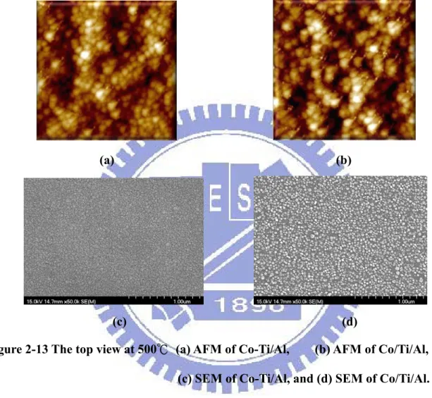
Figure 2-13 The top view at 500℃ (a) AFM of Co-Ti/Al, (b) AFM of Co/Ti/Al, (c) SEM of Co-Ti/Al, and (d) SEM of Co/Ti/Al. ··· 54
Figure 2-14 The surface energy effected on interface reaction. ··· 55
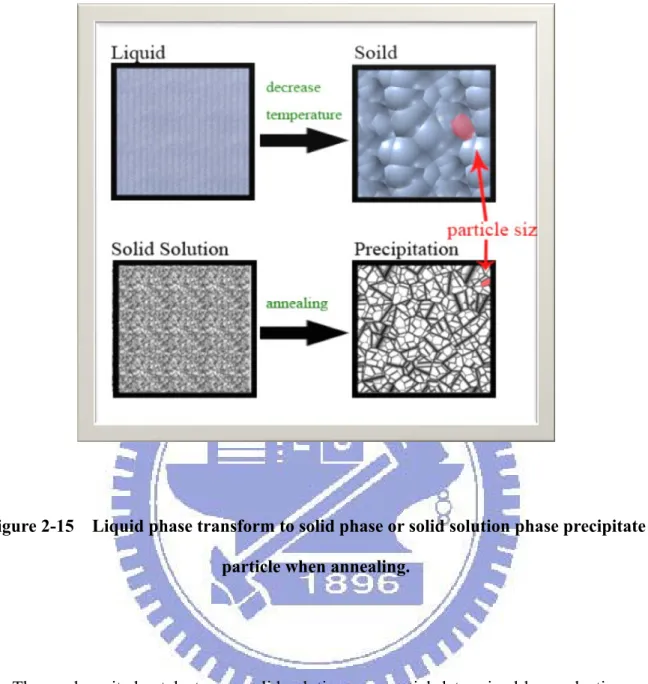
Figure 2-15 Liquid phase transform to solid phase or solid solution phase precipitate particle when annealing. ··· 57
Figure 2-16 The scheme of (a) the nucleation rate, and (b) the growth rate. ··· 58
Figure 2-17 The nucleation rate of Co and Fe. ··· 58
Figure 2-18 The phase diagram of (a) Fe-C, and (b) Co-C. ··· 60
Figure 2-19 The four kinds of catalyst films at 500 to 700℃ (a) RMS (b)particle’s size. ··· 61
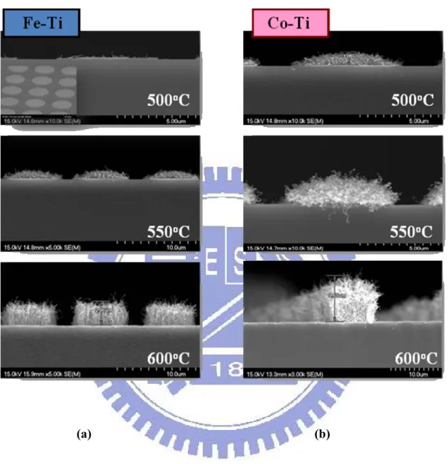
Figure 2-20 The pillar-liked CNTs profile image by SEM by (a) Fe-Ti catalyst (b) Co-Ti catalyst. ··· 64
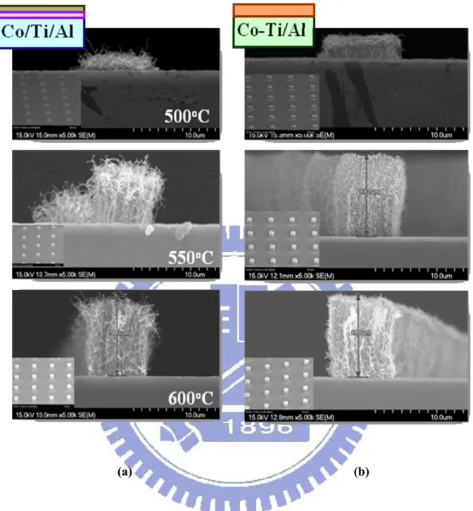
Figure 2-21 The pillar-liked CNTs profile image by SEM by (a) Co-Ti catalyst (b) Co-Ti/Al catalyst. ··· 66
Figure 2-22 The pillar-liked CNTs profile image by SEM by (a) Co-Ti/Al catalyst (b) Co/Ti/Al catalyst. ··· 68
Fiugure 2-23 The CNT growing scheme profile (a) details of reaction on an pattern, (b) details of reaction on a single catalyst particle. ··· 69
xii
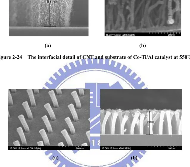
Figure 2-25 The (a) top view and (b) profile of pillar-liked CNTs at high temperature on SEM. Co-Ti/Al for example. ··· 70 Figure 2-26 (a) Raman Spectra by difference catalysts at 550, (b) ID and IG ratios. ··· 71
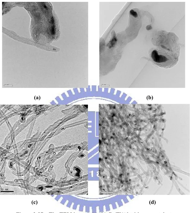
Figure 2-27 The TEM images (a)-(b) Co/Ti/Al tri-layers catalyst (c)-(d) Co-Ti/Al co-deposited catalyst. ··· 72 Figure 2-28 The I-V curves of comparing (a) Fe-Ti and Co-Ti, (b) Co-Ti and Co-Ti/Al, and
(c) Co-Ti/Al and Co/Ti/Al. ··· 74 Figure 2-29 I-V curve of CNTs on Co-Ti/Al and Co/Ti/Al at (a)500℃ (b)550℃ (c)600℃. ·· 76 Figure 2-30 I-V data of CNTs on Co-Ti/Al and Co/Ti/Al at different temperature (a) turn-on
field (b) current density under 7 V/μm. ··· 77 Figure 2-31 Stress testing of CNTs on Co-Ti/Al and Co/Ti/Al. ··· 78 Figure 2-32 The trend of reliability of CNTs on Co-Ti/Al and Co/Ti/Al at different
temperature. ··· 79 Figure 2-33 Profiles of CNTs before and after stress test. ··· 80 Figure 2-34 The (1cmx1cm) illuminated Images by digital camera. ··· 80 Figure 2-35 SEM micrographs of CNTs on Co-Ti/Al growing (a) 10min (b) 30min (c)
60min (d) 90min (e) 120min at 550℃. ··· 83 Figure 2-36 Heights of pillar-like CNTs with different growth time. ··· 83 Figure 2-37 Details of a pattern pillar-like CNTs grown about 10 min. ··· 84 Figure 2-38 (a) Raman analysis with the different growing times and (b) ID/IG ratios with
different growing times. ··· 84 Figure 3-29 The HRTEM images of CNT multiwall with (a) 10min (b) 60min (c) 90min
growth. ··· 85 Figure 2-40 The I-V plots of pillar-like CNTs with different growing times at 550℃. ··· 86 Figure 2-41 Stress testing of pillar-like CNTs with different growing times at 550℃. ··· 87 Figure 2-42 The luminescent images of pillar-like CNTs with different growing times at
xiii
550℃. ··· 87 Figure 2-43 The pillar spacing as the variations in experiment C from 3μm to 30μm, 3μm,
6μm, and 9μm were shown for example. ··· 89 Figure 2-44 The I-V plots of pillar-like CNTs with different pillar spacing (3μm, 6μm,
9μm, 12μm, 15μm, 20μm, 25μm, and 30μm) growing at 550℃. ··· 90 Figure 2-45 Stress testing of pillar-like CNTs with different pillar spacing (3μm, 6μm, 9μm,
12μm, 15μm, 20μm, 25μm, and 30μm) growing at 550℃. ··· 91 Figure 2-46 Luminescent images of pillar-like CNTs with different pillar spacing (3μm,
6μm, 9μm, 12μm, 15μm, 20μm, 25μm, and 30μm) growing at 550℃. ··· 91
Chapter 3:
Figure 3-1 Schematic of a triode field emission pixel. ··· 95 Figure 3-2 Changeable parameters of triode structure in this research. ··· 96 Figure 3-3 The variable gate length was one of parameters. ··· 97 Figure 3-4 The simulations of effects by different gate length (a) 10μm (b) 15μm (c) 20μm
(d) 25μm (e) 30μm. ··· 98 Figure 3-5 The diameter of electron dispersion (lighting size) versus gate length plot. ··· 99 Figure 3-6 The factor of vertical distance (a) oxide was higher than CNTs, (b) oxide was as
high as CNTs (c) oxide was shorter than CNTs. ··· 100 Figure 3-7 The diameter of electron dispersion versus vertical distance. ··· 101 Figure 3-8 The schematic of a short situation occurred because of over height of CNTs. · 102 Figure 3-9 The dispersion of emission electron increased with the gate to emitter length,
the lighting region was (a) 310μm by 1μm gate to emitter length (b) 280μm by 2μm gate to emitter length (c)240μm by 3μm gate to emitter length. ··· 103 Figure 3-10 The dispersion of emission electron will increase with the gate to emitter length.
··· 104 Figure 3-11 The schematic of the shorter length bring more risk of short circuit. ··· 104
xiv
Figure 3-12 Simulations of electron dispersion of 100μm pattern spacing (a) with (c) without gate, and 200μm (b) with (d) without gate. ··· 105 Figure 3-13 The schematic profile of triode gated structure in our research. ··· 105 Figure 3-14 The schematic of electron trajactory (a) without gate structure and (b) with
central gate structure. ··· 106 Figure 3-15 The simulations of different lengths between gate and emitter were (a) 1μm, (b)
1.5μm, (c) 2μm, and (d) 2.5μm. ··· 107 Figure 3-16 The calculated current density of one emitter patter. ··· 109 Figure 3-17 The schematic figure with (a) 200μm pattern spacing and 80V gate voltage by
our simulation with F-N theory, (b) 100μm pattern spacing. ··· 109 Figure 3-18 the F-N theory dominated this experiment, the 100μm would show the superior
uniform dispersion than 200μm. ··· 110 Figure 3-19 The schematic profile and scales of each parameter. ··· 111 Figure 3-20 The process of fabrication of triode field emission structure (a) preparing Si
(100) substrate, (b) 100nm Cr electrode, (c) 1000nm SiO2, (d) Cr gate 100nm, (e)
photo-resistance (PR) coating, (f) developing, (g) clear out the PR, and (h) CNTs growth. ··· 112 Figure 3-21 The mask and top view of optical microscope (a) 200μm, (b)100μm. ··· 113 Figure 3-22 The cross section images of our triode structure by SEM which CNTs growing
time was (a) 10min and (b) 30min. ··· 114 Figure 3-23 Comparing of diode pillar and this simple triode structure. ··· 114 Figure 3-24 (a) The I-V plots of our triode structure with F-N plot inside (b) the logarithm
1
Chapter 1
Introduction
1.1 Overview of Vacuum Microelectronics
1.1.1 History of Vacuum Microelectronics
In 1948, vacuum tubes have been gradually replaced by solid state devices, which tiny volume, low cost, better reliability, and more power efficient transistors were invented by John Bardeen, Walter Bratain, and William Shockley [1.1].
But nowadays, there has been a growing interest in vacuum microelectronics. Some reasons for the increasing interest have to do with the superior theoretical electrical characteristics of the vacuum microelectronic devices over semiconductor devices. The so called vacuum microelectronic devices using the professional micro fabrication technology have been successfully fabricated and gave a new life to vacuum electronics due to great improvements on semiconductor manufacturing technology for the past decades.
“Vacuum state” devices have many superior advantages with respect to the present “solid state” devices, including radiation hardness, temperature insensitivity, and fast drift velocity. For example, there is negligible radiation effect in vacuum devices due to medium being damaged as the electrons fly in the vacuum [1.2].
Moreover, there is no medium for electrons fly in the vacuum, so there is no lattice scattering or bulk carrier generation/recombination. Therefore, the vacuum microelectronic devices can suffer to 500 ℃ or above as long as the structures of the vacuum devices do not destroyed and greatly reduced (nearly eliminated) temperature sensitivity problem which usually comes along with semiconductor devices. Additionally, the saturation drift velocity is limited to less than 3×107 cm/s in all semiconductor due to scattering mechanism whereas the
2
saturation drift velocity in vacuum is limited theoretically to 3×1010 cm/s and practically to
about 6-9×108 cm/s [1.3].
Table 1-1
Comparison between vacuum microelectronics and solid-state electronics.
Items Microelectronics Solid State Microelectronics Vacuum
Current Density 104 – 105 (A/cm2) similar
Turn-on Voltage 0.1 – 0.7 V 5 – 300 V
Structure solid/solid interface solid/vacuum interface Electron Transport in solid in vacuum Electron Velocity 3×10⁷ (cm/sec) 3×10¹⁰ (cm/sec)
Flicker Noise due to interface due to emission Thermal & Short Noise comparable comparable Electron Energy < 0.3 eV a few to 1000 eV Cut-off Frequency < 20 GHz (Si) &
100 GHz (GaAs)
< 100 – 1000 GHz Power small – medium medium – large Radiation Hardness poor excellent
Temperature Effect -30 – 50 °C < 500 °C
Fabrication & Materials well established (Si) & fairly well (GaAs)
not well established
Table 1-1 shows the comparison between vacuum microelectronic and semiconductor devices.Vacuum electronics can be broadly separated into two categories: Thermionic emission or Field emission. The theory of field emission started in 1928, when R. H. Fowler and L. W. Nordheim published the first theory of electron field emission ( Fowler- Nordheim theory) from metals using quantum mechanics [1.4]. The difference concerns the way electrons are emitted from the cathode. Thermionic emission relies on a heated electron emitter, or cathode. The cathode is heated up enough such that the electrons receive enough
3
kinetic energy to leave the surface of the cathode. Field emission, unlike thermionic emission, is possible with a cold cathode. Field emission is a form of quantum tunneling in which electrons pass through a barrier in the presence of a high electric field. This phenomenon is highly dependent on both the properties of the material and the shape of the particular cathode, so that higher aspect ratios produce higher field emission currents. According to the Fowler-Nordheim theory, an applied electric field of approximately 103 V/m is needed for electrons to tunnel through the sufficiently narrow barrier [1.2]. To reach this high field at reasonable applied voltage, it is customary to machine the field emitters into protruding objects to take advantage of field enhancement.
It was not until 1968 when C. A. Spindt camp up with a fabrication method to create very small dimension metal cones that vacuum microelectronic triodes became possible [1.2]. Fig.1-1is a schematic diagram of the triode fabricated by Spindt [1.5]. From the late 1960s to the year 1990, Ivor Brodie, Henry F. Gray, and C. A. Spindt made many contributions to this field. Also, most of research was focused on the devices similar to the Spindt cathode during the past three decades.
Figure 1-1 The SEM micrograph of (a) Spindt type triodes array, (b) Spindt type field emission triode, (c) Emitting way of spindt type triode. [1.5]
4
In 1991, a group of research of the French company LETI CHEN reported a microtip display at the fourth International Vacuum Microelectronics Conference [1.6]. Their display was the first announcement of a practical vacuum microelectronic device. From then on, a great amount of researchers all over the world devoted themselves to this interesting, challenging, and inventive field. Part of the work focused on fabricating very small radius silicon tip by utilizing modern VLSI technology [1.7-1.8]. Some of them increased the emission current by coating different metals, such as W, Mo, Ta, Pt etc., even diamond on field emission arrays [1.9-1.10]. Different device schemes also have been proposed to enhance the emission current density, stability, and reliability.
1.1.2 Theory Background
In quantum mechanical, electron field emission is a tunneling phenomenon of electrons extracted from the conductive solid surface, such as a metal or a semiconductor, where the surface electric field is extremely high.
If a sufficient electric field is applied on the emitter surface, electrons will be emitting through the surface potential barrier into vacuum, even under a very low temperature. On the other hand, thermionic emission is the hot electron emission under high temperature and low electric field. Fig. 1-2(a) demonstrates the band diagram of a metal-vacuum system.
Here W0 is the energy difference between an electron at rest outside the metal and an
electron at rest inside, whereas Wf is the energy difference between the Fermi level and the
bottom of the conduction band. The work function φ is defined as φ = W0 - Wf. If an external
bias is applied, vacuum energy level is reduced and the potential barrier at the surface becomes thinner as shown in Fig. 1-2(b).
5
Figure 1-2 Energy diagrams of vacuum-metal boundary: (a) without external electric field; and (b) with an external electric field.
Vacuum
Metal
Bottom of conduction band Fermi Level ψ E Vacuum Level Fermi Level ψ Vacuum Level X1= 0 X2 (b) (a) Wf W0 E W0
W
6
Then, an electron having energy “W” has a finite probability of tunneling through the surface barrier. Fowler and Nordheim derive the famous F-N equation (1.1) as follow [1.2]:
( )
exp[ 2 ( )/ ] 3 2 2 E y v b y t aE J φ φ − = , (1-1)where J is the current density (A/cm2). E is the applied electric field (V/cm), φ is the work function (in eV), a = 1.56×10⁻⁶, b = -6.831×10⁻⁷, y = 3.79x10-4×10-4E1/2/φ, t2(y)~1.1 and v(y)
can be approximated as [1.10] v(y)=cos(0.5πy), (1-2) or ( ) 0.95 2. y y v = − (1-3)
Typically, the field emission current I is measured as a function of the applied voltage V. Substituting relationships of J = I/α and E = βV into Eq.(1-1), where α is the emitting area and β is the local field enhancement factor of the emitting surface, the following equation can be obtained exp[ ( ) ] ) ( 2 3 2 2 2 V y bv y t V A I β φ φ αβ − = . (1-4)
Then taking the log. form of Eq. (1-4) and v(y) ~ 1
] 2.97 10 ( ( )) ) ( 10 54 . 1 log[ ) log( 2 3 7 2 2 6 2 V y v y t V I β φ φ αβ − × × = − , (1-5)
from Eq. (1-5), the slope of a Fowler-Nordheim (F-N) plot is given by
2.97 10 ( 2) 3 7 β φ × = ≡slopeFN S , (1-6)
7
The parameter β can be evaluated from the slope S of the measured F-N plot if the work function φ was known
2.97 10 ( 2) 3 7 S φ β =− × (cm-1), (1-7)
The emission area α can be subsequently extracted from a rearrangement of Eq.(1-5)
exp( 9.89)exp(6.53 10 ) 10 4 . 1 ) ( 2 3 7 2 6 2 V V I β φ φ β φ α − × × = − (cm2). (1-8)
For example, the electric field at the surface of a spherical emitter of radius r concentric with a spherical anode (or gate) of radius r+d can be represented analytically by
( ) d d r r V E= + , (1-9)
Though a realistic electric field in the emitter tip is more complicated than above equation, we can multiply Eq.(1-9) by a geometric factor β` to approximate the real condition.
Etip ≡function of (r,d) =β` ( ) d d r r V + , (1-10)
where r is the tip radius of emitter tip, d is the emitter-anode(gate) distance and β` is a geometric correction factor [1.11].
For a very sharp conical tip emitter, where d >> r, Etip approaches to β`(V/r). And for
r>>d, Etip approaches to β`(V/d) which is the solution for a parallel-plate capacitor and for a
diode operation in a small anode-to-cathode spacing.
As the gated FEA with very sharp tip radius, Eq. (1-10) can be approximated as:
Etip =β`(V/r). (1-11)
8
Etip =βV =β`(V/r), and β`= βr. (1-12)
The tip radius r is usually in the range from a few nm to 50 nm, corresponding to the parameter β` ranging from 10-1 to 10-2.
Besides, transconductanceg of a field emission device is defined as the change in anode m
current due to the change in gate voltage [1.1]. g C m V I g ∂ ∂ = |Vc, (1-13)
Transconductance of a FED is a figure of merit that gives as an indication of the amount of current charge that can be accomplished by a given change in grid voltage. The
transconductance can be increased by using multiple tips or by decreasing the gate-to-cathode spacing for a given anode-to-cathode spacing.
The following approaches may therefore be taken to reduce the operating voltage of the field emission devices according to the equations above mentioned:
a. Narrow the cone angle for increasingβ
b. Reproducibly sharpen the tips to the atomic level for increasingβ c. Choose the tip material which has the lower work function (φ)
9
1.2 Applications of Vacuum Microelectronic Devices
Due to the superior properties of vacuum microelectronic devices, potential applications include high brightness flat-panel display [1.12-1.16], high efficiency microwave amplifier and generator [1.17-1.19], ultra-fast computer, intense electron/ion sources [1.20-1.21], scanning electron microscopy, electron beam lithography, micro-sensor [1.22-1.23], temperature insensitive electronics, and radiation hardness analog and digital circuits
1.2.1 Vacuum Microelectronic Devices for Electronic Circuits
Either vacuum or solid-state devices can generate power at frequency in the GHz range. Solid-state devices, such as impact avalanche transit time (IMPATT) diodes, Si bipolar transistors, and GaAs FETs [1.24], are typically used in the lower power (up to 10 W) and frequency (up to 10 GHz) range. Vacuum devices still remain the only technology available for high power and high frequency applications. These devices include traditional multi-terminal vacuum tubes, like triodes, pentodes, and beam power tubes, and distributed-interaction devices, such as traveling wave tubes (TWTs), klystrons, backward-wave oscillators (BWOs).
The performance of FEAs in conventionally modulated power tubes, like TWT, is determined primarily by their emission current and current density capability. On the other hand, application of FEAs in the microwave tubes in which modulation of the beam is accomplished via modulation of the emission current at source, such as capacitance and transconductance. Successful operation of a gated FEA in a 10 GHz TWT amplifier with conventional modulation of electron beam has been demonstrated by NEC Corporation of Japan [1.25]. The amplifier employed a modified Spindt-type Mo cathode with circular emission area of 840 μm in diameter. The modified cathode structure incorporated a resistive poly-Si layer as a current limiting element. The emission current from the cathode was 58.6
10
mA. The prototype TWT could operate at 10.5 GHz with the output power of 27.5 W and the gain of 19.5 dB. The bandwidth of the tube was greater than 3 GHz. The prototype was operated for 250 h.
1.2.2 Field Emission Displays
Among wide range applications of the vacuum microelectronics, the first commercial product could be the field emission flat-panel display. The field emission fluorescent display is basically a thin cathode ray tube (CRT), which was first proposed by SRI International and later demonstrated by LETI [1.6].
Various kinds of flat-panel displays, such as liquid crystal display (LCD), electroluminescent display (EL), vacuum fluorescent display (VFD), plasma display panel (PDP), and light emitting display (LED), are developed for the better characteristics of small volume, light weight, and low power consumption. LCDs have become the most popular flat panel displays, however, LCDs have some drawbacks, such as poor viewing angle, temperature sensitivity and low brightness. As a result, some opportunities still exist and waiting for the solutions from other flat panel displays such as FED.
FED features all the pros of the CRTs in image quality and is flat and small volume. The schematic comparisons are revealed in Fig. 1-3 [1.24]. The operation of CRTs involves deflection of the beam in such a way that the electron spot scans the screen line-by-line. In FEDs, multiple electron beams are generated from the field emission cathode and no scanning of beams is required. The cathode is a part of the panel substrate consists of an X-Y electrically addressable matrix of field emission arrays (FEAs). Each FEA is located at the intersection of a row and a column conductor, with the row conductor serving as the gate electrode and the column conductor as the emitter base. The locations where the rows and columns intersect define a pixel. The pixel area and number of tips are determined by the desired resolution and luminance of the display. Typically, each pixel contains an FEA of
11
4-5000 tips. The emission current required for a pixel varies from 0.1 to 10 μA, depending on the factors such as the luminance of the display, phosphor efficiency and the anode voltage.
(a)
(b)
Figure 1-3 The schematic diagram of (a) conventional CRT and (b) comparison between CRT and FED. [1.24].
12
Compared to the active matrix LCDs and PDPs, FEDs are energy efficient and could provide a flat panel technology that features less power consumption. They can also be cheaper to make, as they have fewer total components. Moreover, FEDs could generate three times the brightness with wilder viewing angle at the same power level. Full color FEDs have been developed by various research groups from different aspects such as Motorola, PixTech, Futaba, Sony/Candescent, Samsung, and Canon-Toshiba are presently engaged in commercially exploiting FEDs. the products of above mentioned companies are shown in Fig. 1-4.
13 (a) (b) (c) (d) (e) (f)
Figure 1-4 The full color FED products: (a) Motorola 5.6” color FED based on Spindt-type , (b) Pixtech 5.6” color FED based on Spindt-type, (c) Futaba 7” color FED based on Spindt-type, (d) Sony/Candescent 13.2” color FED based on Spindt-type, (e) Samsung 32“ under-gate CNT-FED, and (f) Canon-Toshiba 36” SED-TV.
14
1.2.3 Cathode Structure and Materials for Field Emission Displays
Field emission display is one of the most promising emissive type flat-panel displays, which can overcome the drawbacks of TFT-LCD, such as poor viewing angle, temperature sensitivity, low contrast and low brightness. This section introduces some novel cathode structures and synthesizes these novel emitter materials for FED operations
1.2.3.1 Spindt-type Field Emitters
The “Spindt” cathode was first proposed by C. A. Spindt in 1968 [1.25]. The scanning electron microscope (SEM) image of a spindt type field emission triode has been shown in Fig. 1-1 agian. It was first invented by Spindt of SRI and improved for the electron source of high-speed switching devices or microwave devices [1.2]. In 1970s, Meyer of LETI applied Spindt-typed emitters for a display and introduce a resistive layer as the feedback resistance to stabilizing the field emission from Spindt-type emitters [1.26].
Figure 1-1 The SEM micrograph of (a) Spindt type triodes array, (b) Spindt type field emission triode, and (c) Emitting way of spindt type triode. [1.5]
15
The structure of Spindt-type FED includes a substrate, a cathode electrode of an electron emission unit formed thereon having a substantially conical shape, and a gate electrode of a lead-out electrode stacked on a substrate around the cathode electrode having an insulating layer. In the Spindt type FED a voltage is applied between the cathode electrode and the gate electrode in a vacuum to thereby produce a high electric field. As a result, electrons are emitted from a tip end of the cathode electrode through the electron emission mechanism in an electric field. In addition, the Spindt-type FED has a conical electron emission portion formed on a cathode electrode. It higher electron drawing efficiency since the electron emission portion is arranged in the vicinity of the center of the gate electrode where the electric field is most concentrated, and the directivity of electron emission is regular.
The merits of the Spindt-type field emitters are summarized as following: (1) High emission current efficiency, more than 98 % anode current to cathode current can be achieved for the symmetric structure of Spindt tip and the gate hole, the lateral electric field to the metal tip can be cancelled out. (2) The fabrication is self-aligned, easy process; uniform field emission arrays can be fabricated easily. Some research groups have successfully fabricated commercial FED products based on Spindt-type field emitters such as motorola, Pixtech, Futaba and Sony/Candesent.[1.27], the products of above mentioned companies are shown in Fig. 1-4.
However, there are some drawbacks of Spindt-type field emitters when fabricating Spindt-type FED such as (1) High gate driving voltage required; for a Spindt-type field emission triode with 4 μm gate aperture, the driving voltage is typically more than 60 V, which results in the high cost of the driving circuits. To reduce the gate driving voltage, frontier lithography technologies such as E beam lithography must be applied to reduce the gate aperture to the sub-micron level. (2) The emission property degrades for the chemically instable of the metal tips. (3) Huge, expensive high vacuum deposition system required during fabricating large area Spindt-type FED.
16
1.2.3.2 Silicon Tip Field Emitters
An alternative approach to fabricate tip type field emitters is to fabricate the Si tip field emitters based on the semiconductor fabricating process. Figure 1-5 depicts the SEM micrographs of Si tips array, Si tip field emission triodes array formed by chemical mechanical polishing (CMP) [1.28] and double gate of Si field emitter arrays [1.29]. Symmetric device structure and similar advantages with Spindt-type field emitters can be obtained. However, high temperature oxidation sharpening process prohibits Si tip from large area fabrication
(a)
(b)
Figure 1-5 (a) Si tip formed by isotropic etching and (b) Si tip field emission triodes array formed by CMP [1.28] [1.29]
17
1.2.3.3 Surface Conduction Electron Emitters
A surface conduction electron emitter (SCE) display is a flat panel display technology that uses surface conduction electron emitters for every individual display pixel. The surface conduction emitter emits electrons that excite a phosphor coating on the display panel, the same basic concept found in traditional CRT televisions. The key technology to the electron emitters begins with the creation of an extremely narrow slits (~ several nanometers) between two electric poles in thin film of PdO (Palladium Oxide). Electrons are emitted from one side of the slit when approximately 10 V of electricity are applied. Some of these electrons are scattered at the other side of the silt and accelerated by the voltage (approximately 10 kV) applied between the glass substrates; causing light to be emitted when they collide with the phosphor-coated glass plate. The PdO film is coated by inject printing or screen-printing technology and this is a low cost process. This means that SEDs use small cathode ray tubes behind every single pixel (instead of one tube for the whole display) and can combine the slim form factor of LCDs and plasma displays with the superior viewing angles, contrast, black levels, color definition and pixel response time of CRTs. The major problem of SED is that the efficiency is still low and the power consumption will be very high. Fig. 1-6 shows the SEM image of SCE cathode array, structure and a 36-inch display of SED [1.30][1.31].
The research of SED was began by Canon in 1986, and in 2004, Toshiba and Canon announced a joint development agreement originally targeting commercial production of SEDs. In October 2006, Toshiba's president announced the company plans to begin full production of 55" SED TVs in 2007. In December 2006, Toshiba President and Chief Executive Atsutoshi Nishida said Toshiba is on track to mass-produce SED TV sets in cooperation with Canon by 2008.
18
t
(b)
(c)
Figure 1-6 (a) The structure of SED, (b) SEM image of SCE cathode array, and (c) A 36-inch prototype of surface conduction electron emitter display. [1.30] [1.31]
19
1.2.3.4 Carbon and Nano-sized Emitters
So-called carbon nanotubes (CNTs) is the nano-sized and carbon emitters, is known to be useful for providing electron emission in field emission devices, such as cold cathodes that are used in a field emission display. Although Spindt-type emitters are generally used for FEDs, they still have a problem in that the life span of micro-tips is shortened due to atmospheric gases or a non-uniform field during a field emission operation. Moreover, the work function of the conventional metal emitters is too high to decrease a driving voltage for field emission. To overcome the problem, CNTs which have a substantially high aspect ratio, excellent durability due to their structure and excellent electron conductivity have been instead of Spindt-type emitters for field emission. CNTs are are anticipated to be an ideal electron emission source since they feature a low work function, the resultant electron emission source can be driven by applying low voltages, and the method of fabricating the same is not complicated. They will thereby offer advantages to realize a large size panel display in terms of view angle, definition, power consumption, and temperature stability.
20
1.3 Field Emission Properties of Carbon Nanotubes
Since the discovery of carbon nanotubes (CNTs) by Iijima in 1991, [1.32] CNTs have attracted considerable interests because of their unique physical properties and many potential applications [1.33]. CNTs have numerous potential applications in nanoelectronics, nanometer-scale structural materials, hydrogen storage, field-emission devices, and so on. Among these applications, CNTs seem to be very promising as electron emitters for field-emission displays (FEDs).
1.3.1 The Synthesis Methods of Carbon Nanotubes
Carbon nanotubes (CNTs) have been extensively investigated for the synthesis using arc discharge, laser vaporization, pyrolysis, solar energy, and plasma-enhanced chemical vapor deposition (CVD), for its unique physical and chemical properties and for applications to nanoscale devices. However, common methods of CNT synthesis include: (1) arc-discharge [1.34], (2) laser ablation [1.35], (3) thermal CVD [1.36-1.38], and (4) plasma enhanced CVD [1.39][1.40].
The laser ablation can synthesize pure carbon nanotubes in high fabrication temperature, but large scale display panel can not be fabricated in the high fabrication temperature above the melting point of glass substrate. The arc discharge can synthesize carbon nanotubes in shorter fabrication times, but it has some issues, such as (1) poor purity, (2) hard to control growth orientations of carbon nanotubes, and (3) poor emission uniformity.
Compared to laser ablation and arc discharge, using CVD for carbon nanotube growth has some features, such as (1) high purity carbon nanotubes, (2) selective growth only for catalyst metal, (3) controlling growth direction, and (4) much suitable to semiconductor fabrication procedure. However, with the display technology trend, it is the time for large
21
panel display. We need to synthesize carbon nanotubes using CVDs on large panel substrates. For this reason, carbon nanotube growth at low temperatures is unavoidable, but the purity of carbon nanotubes at low temperatures is poor. So, we still try some methods to increase growth rates at low temperatures, such as (1) multilayer catalysts, (2) plasma CVDs, (3) post-treatment, and so on.
1.3.2 Structure and Properties of Carbon Nanotubes
CNTs can be divided into two categories. The first is called multiwalled carbon nanotubes (MWNTs). MWNTs are close to hollow graphite fibers [1.41], except that they have a much higher degree of structural perfection. They are made of sheets of carbon atoms with a cylindrical shape and generally consist of co-axially arranged 2 to 20 cylinders「Fig. 1-7(b)」. The interlayer spacing in MWNT (d(002) = 0.34 nm) is slightly larger than that in
single crystal graphite (d(002) = 0.335 nm) [1.42]. This is attributed to a combination of tubule
curvature and van der Waals force interactions between successive garphene layers. The second type of the nanotube is made up of just a single layer of carbon atoms. These nanotubes are called the single-walled nanotubes (SWNTs) and possess good uniformity in diameter about 1.2 nm「Fig. 1-7(a)」. They are close to fullerenes in size and have a single-layer cylinder extending from end to end [1.43][1.44].
22
(a)
(b)
Figure 1-7 High-resolution transmission electron microscopy images of (a) SWNTs, and (b) MWNTs. Every layer in the image (fringe) corresponds to the edges of each cylinder in the nanotube assembly [1.42].
Most experimentally observed CNTs are multi-walled structures with outer most shell diameters exceeding 10 nm. Since current conduction in a MWNT is known to be mostly confined to the outermost single-walled nanotube and since band gap of a SWCNT varies inversely with its diameter, MWNTs are metallic in nature. SWNTs can be either metallic or semiconducting depending on the way the roll-up of the graphene sheet occurs - an aspect termed as Chirality, and if all the roll-up types are realized with equal probability, 1/3 of the SWNTs end up being metallic and 2/3 semiconducting. The structure of a SWNT can be conceptualized by wrapping a one-atom-thick layer of graphite called graphene into a
23
seamless cylinder. The way of the graphene sheet is wrapped is represented by a pair of indices (n,m) called the chiral vector. The integers n and m denote the number of unit vectors along two directions in the honeycomb crystal lattice of graphene. If m=0, the nanotubes are called "zigzag". If n=m, the nanotubes are called "armchair". Otherwise, they are called "chiral". Fig. 1-8 depicts these structures of a SWNT [1.45] [1.46].
CNTs have been attracting much attention for their unique physical and chemical properties such as high mechanical strength, chemical stability, high aspect ratio, super-therml conductivity, and electron emission properties [1.47] [1.48]. CNTs could be one of the strongest and stiffest materials known, in terms of tensile strength and elastic modulus respectively. This strength results from the covalent sp2 bonds formed between the individual carbon atoms. The highest tensile strength an individual multi-walled carbon nanotube has been tested to be is 63 GPa [1.49]. Under excessive tensile strain, the tubes will undergo plastic deformation, which means the deformation is permanent. This deformation begins at strains of approximately 5% and can increase the maximum strain the tube undergoes before fracture by releasing strain energy. For the thermal conductivity of CNTs , it is predicted that carbon nanotubes will be able to transmit up to 6000 watts per meter per kelvin at room temperature; compare this to copper, a metal well-known for its good thermal conductivity, which only transmits 385 W/m/K. The temperature stability of carbon nanotubes is estimated to be up to 2800 degrees Celsius in vacuum and about 750 degrees Celsius in air [1.50].
24
(a)
(b)
Figure 1-8 Molecular models of SWNTs with (a) chiral vector (b) the categories of the configuration [1.45] [1.46].
25
1.3.3 Potential Applications of Carbon Nanotubes
Since the discovery of CNTs in 1991, CNTs had attracted much attention for their unique physical and chemical properties. Their extensively potential applications lead them to become a super star of nano technology, which cover: (1) Chemical sensor [1.51], (2) IR detector, (3) Nano-conducting Wire, (4) Vehicles for Hydrogen Storage [1.52], (5) Field Effect Transistor [1.53], (6) Field Emission Display (FED), (7) Probe of AFM and etc.
In the wide-ranging applications of CNTs, FED arouses researchers’ interest particularly. In virtue of the superior field emission characteristics, CNTs are applied to the emitting source of cold cathode. The advantages of FED are its low response time, wide view angle, high brightness, high working temperature range and well combination with mature phosphor technology. However, a major problem needs to be solved in this field. It is not allowed to effectively analyze CNTs on a flat panel at relatively lower temperature (<500˚C) and this barrier restriction obstructs the development of CNT-FED so far. The products of CNTs FED is shown in Fig. 1-9.
26
Figure 1-9 (a) Schematic structure of the fully sealed 128 lines matrix-addressable CNT-FED. (b) Cross section SEM image of CNT cathode from Samsung’s FED.(c) A 4.5-inch FED from Samsung, the emitting image of fully sealed SWNT-FED at color mode with red, green, and blue phosphor columns. (d) A prototype of 5” CNT flat panel display by Samsung. [1.54]
(a)
(c) (d) (b)
27
1.4 Motivation
For technological commercialization of products today, the cost is the most important issue. The main concern for manufactures is cost down. It is worth noted that lower cost will provide more advantages for a product. In our research of CNT field-emission backlight unit (FE-BLU), we ensure that if the cost of field-emission backlight unit (FE-BLU) continuously decreases, it can even replace the traditional light bulbs or light-emitting diode (LED) in the future. So the following motivation will focus on decreasing the cost and increasing the quality of CNT FE-BLU.
Nowadays, the backlight unit of liquid crystal display (LCD) is CCFL, but CCFL backlight system contains several components for providing planar and uniformity illumination. The following are designs of LED-BLU:
1. Reflection sheet is used to reflect the light beam of wrong direction from the lamp. 2. Light guide panel is used to transform spot or linear light source to planar light
source.
3. The prism sheet and diffusion sheet are playing the crucial roles in spreading the brightness.
Fig. 1-10 shows the complex system of LED backlight unit on LCD below [1.55] [1.56]. The uniformity become better due to the uniformity-assisted layer of backlight system, but thickness and cost increase obviously. For a LCD, the cost of backlight system on the total cost is about 14% for 17inch TFT-LCD, and 21% for 32inch TFT-LCD, which are shown in Fig. 1-11 [1.57]. As this result, we could easily to make a prediction that we will require more cost on backlight system for a larger size TFT-LCD.
28
(a)
(b)
(c) (d)
Figure 1-10 The profile of LED backlight system (a) shows names of every sheet. [1.55] (b) direction of light beams in backlight system. (c) bottom lighting type of backlight system. (d) edge lighting type of backlight system. [1.56]
29
(a)
(b)
30
Instead of LED-BLU, FE-BLU is another aspect for illumination. Comparing between LED and FE backlight system, we could observe easily few advantages of FE-BLU shown below:
1. The efficiency of FE-BLU is not affected by thermal-effect. Since it is a proto-type of vacuum microelectronic. But thermal-effect give rise to degradation of the brightness or efficiency of LED decrease obviously.
2. FE-BLU is a planar light source showing a better feasibility for larger scale as compare with LED spot light source.
3. For TFT-LCD, using FE-BLU will reduce cost of backlight system and decrease the thickness of display as well.
In our research, we have chose the carbon nanotubes as the emitters of FE-BLU because of some superior properties of CNTs for field-emission. One of the superior properties is low work function ( ~5eV ), high conductivity, small tip of radius curvature, low turn-on electric-field, and high emission current density. Another properties are high chemical stability and high mechanical strength, so CNTs emitter is still stable under high electric-field and current density.
Although CNTs have superior field emission characteristics, there are still some drawbacks needed to be overcome, i.e. uniformity and reliability. The degradation of field emission current and brightness due to week adhesion between CNTs and substrates will result in poor reliability. Problem of uniformity is caused by screening-effect, which is determined by dense of emission emitters. The screening-effect is shown in the Fig. 1-12, indicating that the effective field is affected by the height and density of emitter.[1.58]
31
(a) (b)
Figure 1-12 The screening-effect occurred (a) because of height (b) because of distance between emitter sites [1.58].
(a)
(b)
Figure 1-13 Improvement of Luminescent Uniformity via Synthesizing the Carbon Nanotubes on an Fe–Ti Co-deposited Catalytic Layer (a) conventional catalyst (b) co-deposited catalyst [1.62].
Under 7.7 V/μm Under 7.7 V/μm
32
There are many ways to solve problem of reliability. One is mechanical coating on grown CNTs, such like spin-on-glass (SOG) coating and polymethyl methacrylate (PMMA) coating [1.59][1.60]. Another is CNT printing with Zinc powder mixture [1-61]. Although two method improve the adhesion of CNTs on substrate, it is also increase the cost due to a complex step in the procedure. The way provides with both increasing reliability and keeping low cost is co-deposition of catalyst and buffer layer. Co-deposition means that we produce a solid-solution of catalyst and one buffer metal. In our group, we already got a result of co-deposited catalyst and it really improved the reliability shown in Fig. 1-13 [1-62].
Uniformity is also a very important issue of CNT FE-BLU. There were a lot of ways to enhance uniformity, such as (a) growing CNTs on AAO[1.63], (b) plasma post-treatment[1.64], (c) elastomer or biasing printing[1.65][1.66]… and so on. Here we use the patterned pillar-like CNTs improving the uniformity of emitters. CNT pillar arrays have well-control density and morphology of CNTs, and, moreover, it has been reported that the screening-effect of CNTs can be effectively reduced by the density control of the pillars. Therefore, not only the field emission characteristics can be enhanced from the compromise of screening-effect and emitter sites, but also the uniformity will slightly be enhanced from the decreasing of screening-effect. By using pillar-like CNTs as a light source for BLU, high brightness and excellent uniformity could be achieved by easy and cheap process.
In the growth reaction of CNTs, the diffusion of carbon in the catalyst metal has been believed to be the rate-determining step. The growth rate of CNTs can be described by an Arrhenius equation that the activation energy is the diffusion energy of carbon in the metal [1.67]. Plasma-enhance chemical vapor deposition (PECVD) is more suitable method for CNT synthesis because PECVD has the much lower activation energy compared to thermal CVD [1.68]. However, PECVD has some drawbacks, such like poor plasma uniformity, and hard to fabricate large panel display or large-size BLU.
33
thermal CVD (TCVD) in our study. It has been investigated that the nano-size catalyst could enhance CNTs growth at low temperature because nano-size catalyst particles are more active compared to bulk catalyst and the melting point of particles decrease as their sizes decrease [1.69][1.70]. The following Fig. 1-14 shows surface diffusion or surface pre-melting of nano-size particles takes place when the temperature is raised above 500ْ C whose temperature is close to 0.4Tm [1.70].
A multilayer catalyst, Co/Ti/Al, was successfully employed to synthesize CNTs at 550℃ and 500℃ by thermal CVD previously. Following this result, we could fabricate CNTs on the glass coated with electrode or indium tin oxide (ITO), for large area application.
Figure 1-14 In-situ TEM images recorded from a region of capped Pt nano-crystals at various specimen temperatures. Surface diffusion or surface pre-melting of nano-size particles takes place when temperature is raised about 0.4Tm.
34
The normal triode gate structure is shown in Fig. 1-15[1.71][1.72].The phosphors provide high efficiency into light by bombardments of electrons at enough high voltages of the anode plate. For field emission display (FED), there is a problem of triode gate structure, i.e. cross-talk noise, which is due to the electron beam spreading caused by gate electrode. Cross-talk noise is a drawback for FED, but it has merits for FE-BLU since the electron spreading would result in large area of beam overlapping, which could improve the uniformity of photo-luminescent images on anode plates. Therefore, uniformity could be enhanced just because of enlargement of cross-talk noise.
(a)
(b)
Figure 1-15 Examples of triode gate structure
35
1.5 Thesis Organization
In Chapter 1, the overview of vacuum microelectronics, basic principles of field emission theory, and research motivations are described.
In Chapter 2, we utilize the Co-Ti/Al (5nm/10nm) co-deposited catalyst compared to other kind of multilayer catalyst from our prior study. The improvements of reliability and uniformity in CNT FE-BLU, and increasing growth rate at low temperature are included to realize the properties and mechanism of Co-Ti/Al co-deposited catalyst thin film.
A simply lateral triode field emission device is fabricated in Chapter 3, we have utilized the cross-talk noise, which is one of the triode FE structure drawback, enhancing the uniformity of backlight unit.
36
Chapter 2
Fabrication of Pillar-like CNT Field Emitters with
Low Temperature Processes
2.1 Introduction
CNTs own some attractive physical and chemical characteristics, like high aspect ratio, adequate work function (~5eV), small tip radius of curvature, good chemical stability, strong mechanical strength, high conductivity, and electron emission properties [2.1-2.2].
However CNT-BLUs exist two crucial problems: one is inadequate lifetime which caused by poor reliability, and the other is bad uniformity which caused by screening-effect.
For reliability, two kinds of issues were observed: (1) abrupt decreases in emission current with increasing electric field and (2) a gradual degradation in emission current with high emission current density for a long period. Several reports indicated the weak adhesion on the interface of CNTs and substrate could cause an abrupt decrease in emission current resulting from a mechanical damage at high electric field [2.3]. Furthermore, high contact resistance between CNTs and substrate could result in a gradual degradation in emission current because of the Joule heat generated in a high resistive contact region [2.4]. Some methods have been reported for improving the adhesion or lowering contact resistance on the interface by post-treatment such as spin-on-glass (SOG) or polymethyl methacrylate (PMMA) coating, and zinc powder mixture [2.5-2.6]. Nevertheless, some of them might increase the complexity of processes and the cost of fabrication.
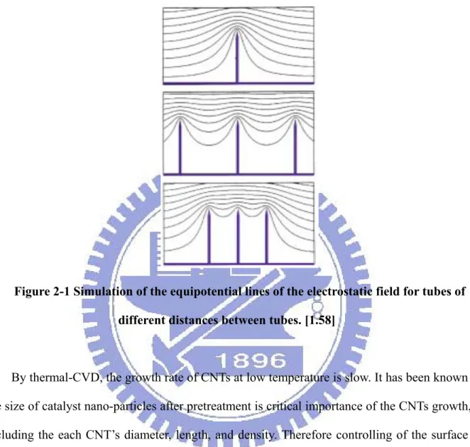
For uniformity issue, the screening-effect and non-uniform height of CNTs play the two most important roles. The simulation of the equipotential lines of the electrostatic field is shown in Fig.2-1 [1.58]. In order to avoid screening-effect, on some reported researches, such
37
as plasma post-treatment [2.7] and growing on AAO substrate [2.8], however these methods also increase the complexity and cost of processes.
Figure 2-1 Simulation of the equipotential lines of the electrostatic field for tubes of different distances between tubes. [1.58]
By thermal-CVD, the growth rate of CNTs at low temperature is slow. It has been known the size of catalyst nano-particles after pretreatment is critical importance of the CNTs growth, including the each CNT’s diameter, length, and density. Therefore controlling of the surface morphology of nano-sized catalyst particles is an essential prior to the CNTs growth. According to Lindemann criterion, the melting point decreases as the catalyst particles sizes reduces as the Fig. 2-2 [2.9].
38
Figure 2-2 Lindemann criterion. [2.9]
And the nano-sized catalyst particles are more active compared with bulk catalyst metals due to surface effect [2.10]. The melting temperature of nano-particles is based on size-dependent cohesive energy by considering the surface effects. The melting temperature of nano-particles (Tmp) is linear to the reciprocal of the crystal size, i.e., Tmp= Tmb (1-C/D),
where Tmb is the melting temperature of the corresponding bulk materials, D is the crystal size,
and C is a material constant. Apparently, the proper determination of D is key issue. The smaller catalyst nano-particles with the lower melting temperature could be utilized to the CNTs growth at low temperature in thermal CVD to increase growth rates. From the AFM image as Fig.2-3 [2.11], the nano-particles of the co-deposited catalyst sample are more uniform and smaller than those of the conventional one. Accordingly, we applied the novel method to CNTs growth at low temperature for understanding the properties and mechanism of co-deposited catalyst.
39
Figure 2-3 AFM of the nano-particles after pretreatment
(a) the pure Fe catalyst layer, and (b) the Ti-Fe co-deposited catalyst layer. [2.11]
The schematic of a typical BLU is shown in Fig.2-4 [2.12] including light source, reflector, light guide, diffuser, and brightness enhancement film (BEF). The light source can be an incandescent light bulb, light emitting diodes(LED), cold cathode fluorescent lamp (CCFL), hot cathode fluorescent lamp (HCFL). All the backlights employ a diffuser and a BEF. The diffuser posited between the light source and the display panel is used to scatter the light for display uniformity. The BEF is used to enhance display brightness. The cost structure of materials for TFT-LCDs is described as Fig. 1-10 [1.57].
If we success to solve the reliability and uniformity problems, CNT-BLU will replace the traditional backlight system of LCD, it will be ensure to decrease amount of cost.
40
Figure 2-4 schematic of a typical backlight unit. [2.12]
Figure 1-10 cost structure of materials for TFT-LCDs of (a) 17inch LCD (b)32inch LCD. [1.57]
First of all, we used titanium as interlayer of the multilayer catalysts for CNT synthesis because it was found the most fitting one for CNT growth at low temperature. Then we fabricated pillar-like CNTs pattered structure on silicon substrate to improve the morphologies. Our group has done some research on multilayer and co-deposited catalysts, but the catalyst are not the optimization for growing CNTs at low temperature. Finally, we accomplished some analysis for the above mentioned. The whole experimental procedures is shown below.