國 立 交 通 大 學
電子工程學系電子研究所碩士班
碩士論文
利用酸式蝕刻氧化鋅奈米線製備氧化鋅奈米管
Preparation and Formation Mechanism of ZnO
Nanotubes by Acidic Etching ZnO Nanowires
研 究 生:姚承佑
指導教授:曾俊元 博士
利用酸式蝕刻氧化鋅奈米線製備氧化鋅奈米管
Preparation and Formation Mechanism of ZnO Nanotubes
by Acidic Etching ZnO Nanowires
研 究 生:姚承佑 Student: Cheng-You Yao
指導教授:曾俊元 博士 Advisor: Dr. Tseung-Yuen Tseng
國立交通大學
電子工程學系電子研究所
碩士論文
A Thesis
Submitted to Department of Electronics Engineering & Institute of Electronics
College of Electrical and Computer Engineering National Chiao Tung University
in Partial Fulfillment of the Requirements For the Degree of
Master In
Electronics Engineering June 2007
Hsinchu, Taiwan, Republic of China
利用酸式蝕刻氧化鋅奈米線製備氧化鋅奈米管
研究生:姚承佑 指導教授:曾俊元 博士
國立交通大學電子工程學系電子研究所
摘要
本論文探討利用簡易的酸式蝕刻來製備較不易成長的氧
化鋅奈米管,已被廣泛研究的低溫製程氧化鋅奈米管的成長
方式,多是使用一個步驟長時間的水熱法製程,對於其半徑
較不易控制,使其大小和高寬比皆不盡理想,藉由分離成長
及蝕刻兩個製程,改善原先奈米結構尺寸較大的問題。
在本論文中,利用調整蝕刻的時間,了解蝕刻時的反應
情形,並改變濃度以得到氧化鋅奈米管的形成和濃度的關
係,使用不同直徑的奈米線來進行同樣的製程,進而得到較
細的氧化鋅奈米結構,討論蝕刻機制。利用高溫加熱製程和
光學性質來驗證其機制,了解機制後再藉此建構出所得到的
氧化鋅奈米結構的蝕刻模型。
Preparation and Formation Mechanism of ZnO
Nanotubes by Acidic Etching ZnO Nanowires
Student: Cheng-You Yao Advisor: Dr. Tseung-Yuen Tseng
Department of Electronics Engineering and Institute of
Electronics National Chiao Tung University
Abstract
ZnO nanotubes were prepared by a simple etching process. The fabrication of ZnO nanotubes was harder than it of nanowires. The general process of ZnO nanotubes is a step hydrothermal method by aging and widely researched because of low reaction temperature. However, it is hard to control the diameter and length of ZnO nanotubes due to the growth process still continue when nanotube structure is form so that the size is larger and the aspect ratio is low. Dividing growth and etching process to improve the issues.
In this thesis, the etching reaction is clearly observed by modifing the etching time, and change of acidic concentration for getting the relation with the formation of ZnO nanotubes. The nanowires with different diameters are used to get thinner nanotubes. At last, the mechanics of etching process is discussed and proved them by annealing experiments and optical properties. According to the mechanics, etching model of ZnO nanotubes by etching its nanowires was established.
誌謝
首先誠摯的感謝指導教授曾俊元老師悉心的教導,並提供了這 個資源充分的環境,使我得以一窺固態電子領域的深奧,與老師和 學長、同學間的討論,提供了我正確的研究方向,使我在實驗中獲 益匪淺。老師對學問的嚴謹更是我輩學習的典範。本論文的完成另 外亦得感謝冠仲、永昇和志洋學長的大力協助。因為有你們的意見 和分析,使得實驗的過程中因而順利且完整。 兩年裡的日子,研究室裡共同的實驗生活,meeting 上的討論、 一同烤肉吃飯的回憶,以及和大家一起買了兩年的便當,感謝家瑋、 信賢、群傑、孟漢、聖裕等學長及秀玉和佳穎學姐的指導和費心,鎮 宇、重毅、俊勝、俊興、士傑、松蒔和我共同努力及成長,以及毅函、 世偉、啟翔、文仁和宏全你們的陪伴讓這兩年的研究生活變得絢麗多 彩。 最後更感謝我的父母,默默地支持和栽培使我能完成這段歷程, 這份喜悅禮是屬於你們的。Contents
Chinese Abstract ... I Abstract...II Acknowledgement... III Contents ... IV Figure Captions... VI Chapter 1 Introduction ...1 1.1 Introduction to ZnO ...11.2 Introduction to ZnO Nanostructures ...3
1.2.1 Processes of ZnO Nanowires ...3
1.2.2 Introduction and Processes of ZnO Nanotubes...8
1.3 Applications of ZnO...11
1.3.1 Optical Properties... 11
1.3.2 Field Emission ...16
1.3.3 Gas Sensing...17
Chapter 2 Experimental...19
2.1 Flow Chart of Preparing Nanotubes ...19
2.2 The Process of Nanotubes...20
2.2.1 Preparation of Nanowires ...20
2.2.2 Etching Process...21
2.2.3 Annealing ...22
2.3 The Experimental Equipment ...24
2.3.1 System of Radio Frequency Magnetron Sputter...24
2.4 The Measured Equipment ...25
2.4.1 Scanning Electron Microscopy ...25
2.4.2 Transmission Electron Microscopy ...25
2.4.3 Cathodluminescence ...26
2.4.4 X-ray Diffraction ...26
Chapter 3 Results and Discussion ...28
3.1 The Preparation before Etching Process ...28
3.1.1 The Characteristics of ZnO Seeding Layer...28
3.1.2 The Characteristics of ZnO Nanowires...29
3.2 The Characteristics of the ZnO Nanotubes ...39
3.2.1 The Influence of Parameters and Scanning Electron Microscopy Analyses...39
3.2.2 Transmission Electron Microscopy Analyses...56
3.2.4 Cathodluminescence Spectra ...58
3.3 The Discussion of Etching Model...61
3.3.1 The Etching Model of ZnO Nanotube ...61
3.3.2 The Etching Models of Other Nanostructures ...66
Figure Captions
Figure 1-1 SEM images of several ZnO nanostructures...3
Figure 1-2 the charts of VLS growth mechanism (a) the formation of a small liquid droplet and the alloying (b) the alloying, nucleation, and growth of the nanowires ...5
Figure 1-3 growth process of the ZnO nanowires by the hydrothermal method...7
Figure 1-4 ZnO nanotubes is fabricated by AAO and CVD process. (a) Low-magnification image of aligned ZnO nanotubes. (b) Tilted view of ZnO nanotube arrays...9
Figure 1-5 (a) TEM image of (b) SAED pattern of ZnO nanotubes synthesized by AAO and CVD process ...10
Figure 1-6 optical spectrum... 11
Figure 1-7 energy level of ZnO defects...13
Figure 1-8 mechanism of the photoluminescence ...14
Figure 1-9 the energy-band diagram of a ZnO grain in cross section. The conduction band (Ec), valance band (Ev), Fermi level (EF), paramagnetic oxygen vacancy (VO•) level, and the diamagnetic VO• • area (hatched) in the grain-boundary depletion region are visualized for a grain with a (a) low and (b) high free-carrier density...15
Figure 1-10 the tunneling phenomenon...16
Figure 2-1 experiment flow ...19
Figure 2-2 The Si substrate deposited ZnO seeding layer...20
Figure 2-3 The Si substrate with ZnO nanowires...21
Figure 2-4 ZnO nanotube synthesized by acidic etching nanowire...22
Figure 3-1 (a) the top view and (b) cross section images of ZnO seeding layer ...29
Figure 3-2 ZnO seeding layer before and after annealing process ...29
Figure 3-3 low resolution SEM images of ZnO nanowires annealed at (a) 900。 C and (b) 750。 C. (c) and (d) are high resolution images...31
Figure 3-4 SEM images of ZnO annealed nanowires (a) O2, 500。C (b) O2, 700。C (c) N2, 500。C (d) N2, 700。C...32
Figure 3-5 XRD pattern of ZnO nanowires...33
Figure 3-6 XRD patterns of ZnO nanowires after annealing in O2 ambient ...34
Figure 3-7 XRD patterns of ZnO nanowires after annealing in N2 ambient ...35
Figure 3-8 CL spectrum of ZnO nanowires...37
Figure 3-10 CL spectra of ZnO annealed nanowires in N2 ambient...38
Figure 3-11 SEM images of ZnO nanostructures after etching for (a) 5min (b) 10min (c) 20 min (d) 40 min (e) 1 h ...41
Figure 3-12 SEM images of ZnO nanostructures after etching for (a) 2 h (b) 4 h (c) 6h (d) 10 h...42
Figure 3-13 SEM images of ZnO nanostructures after etching for (a) 12 h (b) 15 h (c) 17 h ...43
Figure 3-14 SEM images of nanotubes synthesized by aging process...44
Figure 3-15 SEM images of ZnO nanostructure etched for 1h in (a) 1:100000 (b) 1:40000 (c) 1:20000 (d) 3:40000 solution...47
Figure 3-16 SEM images of ZnO nanostructure etched for 12h in (a) 1:100000 (b) 1:40000 (c) 1:20000 (d) 3:40000 solution...48
Figure 3-17 the SEM images of ZnO nanowires etched in (a) 1:1000, 500s (b) 1:100, 50s (c) 1:10, 10s solutions ...49
Figure 3-18 the different diameter (a) 0.05M (b) 0.025M (c) 0.0125M nanowires etched for 12 h ...51
Figure 3-19 SEM images of nanowires annealed at (a) 750。 C and (b) 900。 C, (c) and (d) were etched in default solution for 12 h ...53
Figure 3-20 SEM images of etched for 12 h, nanowires annealed at (a) 300。 C (b) 500。 C (c) 700。 C in O2 ambient before etching ...54
Figure 3-21 SEM images of etched for 12 h, nanowires annealed at (a) 300。 C (b) 500。 C (c) 700。 C in N2 ambient before etching ...55
Figure 3-22 (a) TEM image of ZnO nanotubes (b) HRTEM image of hollow region, the inset is SAED pattern...56
Figure 3-23 the TEM images of different diameters of ZnO (a) 300 nm (b) 100 nm .57 Figure 3-24 XRD patterns of nanowires before and after etching for 12 h...58
Figure 3-25 CL spectra of etched nanowires and nanotubes...60
Figure 3-26 the sample chart of etching process ...61
Figure 3-27 the structure of hexagonal ZnO ...65
Figure 3-28 OH- bonds prevent ZnO (002) face from being etched ...65
Figure 3-29 the complete etching model (a) as grown (b) 20 min (c) 40 min (d) 12 h (e) 15 h...66
Figure 3-30 the etching model of annealed nanowires...67
Figure 3-31 the etching model of ZnO nanowires etched by Vacetic:Vwater=1:1000 solution ...67
Chapter 1
Introduction
1.1 Introduction to ZnO
The nanotechnology have been developed, which contains many kinds of different dimensional nanostructures. The synthesis of 1D, 2D and 3D structures such as nanowires1 , ,2 3, nanorods4 , ,5 6, nanosheets, nanobelts7, nanorings, nanosprings, nanosaws, disks, and nanojunction arrays have been widely researched. The nanostructures have in recent years attracted much attention due to their many unique properties and advantages: higher density of integration, lower cost and less power consumption.
Zinc oxide (ZnO) was II-VI group semiconductor semiconductor with a hexagonal wurtzite structure. The Bravais lattices of hexagonal wurtzite structure are t1 = a/2 (1, 31/2, 0), t2 = a/2 (-1, 31/2, 0), t3 = c (0, 0, 1). The basis of hexagonal wurtzied structure are d1 = (0, 0, 0), d2 = (0, 0, uc), d3 = (0, a/31/2, c/2), d4 = (0, a/31/2, uc+c/2). The lattice constants of ZnO are: a= 3.25A、, c = 5.21A、 and u is a dimensionless parameter (u = 0.345 for ZnO). It has high melting point (1975℃) and high thermal stability. It has a wide and direct band gap of 3.37 eV at room temperature with the large exciton binding energy (60 meV), which makes it a promising candidate for high-efficient, ultraviolet-light-emitting diodes (LEDs).ZnO is well-known as a piezoelectric material in surface acoustic wave (SAW) devices for delay lines, filters, resonators in wireless communication, and signal processing because of its noncentrosymmetric structure 8 . Furthermore, ZnO is bio-safe and biocompatible, and may be used for biomedical applications without coating.
ZnO is also attracting attention for its application to varistors9, transparent high power electronics10, gas-sensing11, hydrogen storage12,13, and solar cells14,15.
Since the discovery of carbon nanotubes (CNTs), many materials were researched to replace CNTs for better properties and behaviors. ZnO is one of many candidates because above-mentioned advantages and characteristics. This subject was focused on the process and etching model of ZnO nanotubes by acidic etching nanowires.
1.2 Introduction to ZnO Nanostructures
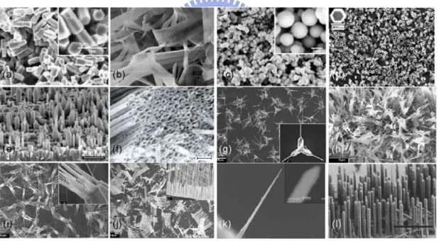
After the first repot of ultraviolet lasing from ZnO nanowires, nanostructures of ZnO have stimulated intensive research. ZnO nanowires and nanorods have been widely studied because of their easy nanomaterials formation and device applications. The nanostructures have in recent years attracted much attention due to their many unique properties so that different morphologies of ZnO-like prisms, tetrapods, and nanotubes have been synthesized successfully. Figure 1-1 is scanning electron microscopy (SEM) images of several ZnO nanostructures16, , ,17 18 19.
Figure 1-1 SEM images of several ZnO nanostructures
1.2.1 Processes of ZnO Nanowires
ZnO nanowires with large exciton binding energy had been studied intensively due to its excellent electronic and optoelectronic properties. In
addition, ZnO nanowires array has been proved to be a promising candidate as a field emitter due to its peculiar properties of high thermal stability and oxidation resistance in harsh environment as compared to CNTs.
ZnO nanowires can be synthesis by different techniques such as VLS, thermal evaporation, MOCVD, electro-chemical deposition method, template enhancement method, etc. Those synthesis techniques look like similar for results. However, there are different advantages and disadvantages. Some need very high temperature which the substrate materials may be melted. Some need high-cost equipment. Even there are several processes to synthesize nanowires but there are main four mechanisms.
Vapor–liquid–solid (VLS)
The VLS process was demonstrated as early as the 1964 by Wagner et al20. This mechanism can be divided into two main steps: the formation of a small liquid droplet and the alloying, nucleation, and growth of the nanowires. Growth is started on a clean, defect-free surface of a substrate. Small metal clusters (diameter below 100 nm) are deposited on the surface to initiate the nanowires growth. The metal clusters absorb the reactants on the substrate. The reactants in vapor phase bond to substrate at the liquid-solid interface after clusters supersaturate. The chart is growth model of VLS.
A suitable temperature in the range of 300~1100。
C is chosen according to the binary phase diagram between the metal and the target material. In a second step, a gas containing the growth material flows through the reaction tube. The nanowires diameter is determined by the size of the metal. The growth rate, however, depends on the supersaturation, which can be influenced by the concentration of precursor vapor and the substrate temperature.
The process is easy to obtain nanowires array with long length, high aspect ratio. However, the high reaction temperature and catalysts metal are issue when the process integrals to VLSI process. Figure 1-2 is a chart of VLS growth mechanism.
Figure 1-2 the charts of VLS growth mechanism (a) the formation of a small liquid droplet and the alloying (b) the alloying, nucleation, and growth of the nanowires
Vapor Solid (VS)
The growth mechanism works in a similar way to the VLS process. However, VS do not need extra metal catalysts and the nanowires can deposition by thermally evaporating a suitable source material near its melting point at cooler temperatures. The gaseous atoms play the role of the catalyst itself.21 In the VS growth mode, control of the NW diameter is accomplished by changing the evaporation, collection temperatures, and the vapor pressure. The process can improve the disadvantage of VLS process, but the aspect ratio and alignment are worst than VLS.
Template-based Synthetic
nano-channel glass, and porous polymer films by CVD, sol-gel, and hydrothermal method. Free-standing nanowires can be obtained by dissolution of the template membrane. The diameter and length are controlled by the films. The advantage of this process is low template, aligned. The issue for semiconductor nanowires fabricated by template method is the crystalline quality. The ZnO nanowire fabricated by template-based method is always amorphous or poly-crystal. To strip template after nanowires growth is also a problem due to the process may damage the nanowires array.
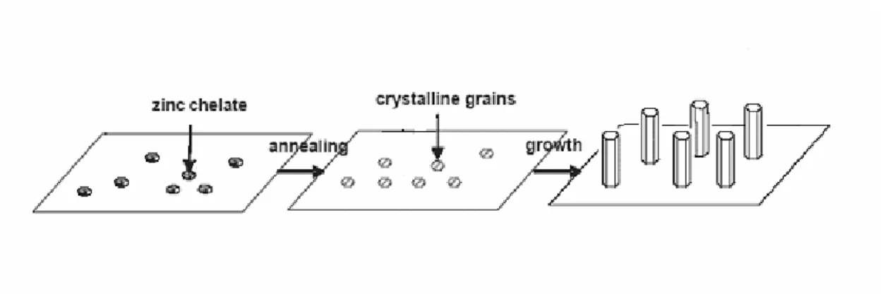
Hydrothermal Method22,23 24,
Even ZnO synthesized by hydrothermal process has lower aspect ratio. Many researchers still use the method to grow ZnO nanowires. The hydrothermal method is low-cost method to fabricate zinc oxide (ZnO) nanowires due to it does not need expensive equipment. This process has other advantages over other growth processes such as catalyst-free growth, low cost, large area uniform production, environmental friendliness, and low reaction temperature to integrate into the microelectronics and plastic electronics. The growth temperature of the ZnO nanowires was below 100。
C. Air flow is not considered due to the reaction is in the solution. The template with ZnO seeding layer was put into an aqueous solution of the zinc nitrate hexahydrate (Zn(NO3)2.6H2O (99.9% purity)) and the hexa-methylenetetramine (HMT,
C6H12N4 (99.9% purity)) in a sealed vessel. The growth process is shown in
Figure 1-3 growth process of the ZnO nanowires by the hydrothermal method
The hydrothermal method is based on the formation of solid phase from a solution, which involves two steps as nucleation and growth. In the nucleation, the clusters of molecules formed undergo rapid decomposition and particles combine to grow up to a certain thickness of the film by heterogeneous reactions at the substrate surface.
For our deposition of ZnO film, zinc nitrate hexahydrate (Zn(NO3)2.
6H2O (99.9% purity) ) is used as source of zinc. When hexamethylenetetramine
(HMT, C6H12N4, (99.9% purity)) was added to the solution, no precipitate
occurs as they were mixed together initially. With the increase of temperature, the HMT begins to decompose into ammonia and then Zn(OH)2 occurred . For
this solution was heated, precipitation on the substrate forms ZnO nuclei, thus ZnO film grows from the nuclei on the substrate. These can be represented by the following reactions:
approach without involving catalysts or templates provides a promising option for the large-scale production of well-dispersed one-dimensional nanostructured materials.
1.2.2 Introduction and Processes of ZnO Nanotubes
The nanotube is also one-dimensional structure and provides larger surface area and high aspect ratio. The research of ZnO nanotubes are less than ZnO nanowires due to the process of ZnO nanowires is easier. However, nanotube structure is still studied in order to improve the properties of nanowires in many applications.
The process of ZnO nanotubes is similar to that of ZnO nanowires but changing some parameters. It is also fabricated by chemical vapor deposition, AAO25, hydrothermal method. Like ZnO nanowires, the chemical vapor deposition26 and aluminum oxide template27 can provide larger aspect ratio and well-aligned than hydrothermal method. ZnO nanotubes synthesized by AAO and CVD process are well-aligned and have very high aspect ratio (Figure 1-4). However, the issue of AAO process is still reserved. The nanotubes align was merged with each other after AAO strip process. The grown ZnO nanotubes are poly-crystalline (Figure 1-5). It means the properties are worst than single-crystalline ZnO nanotubes. The nanotubes synthesized by CVD process is single-crystalline but need higher temperature. The hydrothermal method is low-cost and low temperature ZnO nanotube was fabricated by hydrothermal process is mainly researched.
ZnO nanotubes were widely researched after Vayssieres et al.28 reported the synthesis of ZnO tubes in aqueous solution by aging. The process is like the process of ZnO nanowires by hydrothermal, just only reaction time is longer than nanowires growth. It is easy as nanowires process. However, the diameter
and length are hard to control due the nanotube structure is fabricated after the growth process ends. The diameter of tubes Vayssieres reported was 1~2 μm. The diameter of the tubes other researcher reported was 0.5~1μm.
For controlling the morphology of nantubes, divide the hydrothermal method is an easy process. It is known that the diameter and length of ZnO nanowires are related to the reaction time and solution concentration. Instead of aging process, the nanotubes are fabricated by acidic etching the nanowires. It avoids the nanotube morphology is not controllable due to the reaction time is too long.
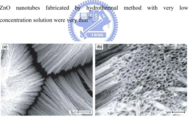
There is other method to grow small diameter of ZnO nanotubes. The researchers deposit ZnO seeding layer by pulsed laser deposition (PLD). The ZnO nanotubes fabricated by hydrothermal method with very low concentration solution were very thin29.
Figure 1-4 ZnO nanotubes are fabricated by AAO and CVD process. (a) Low-magnification image of aligned ZnO nanotubes. (b) Tilted view of ZnO nanotube arrays.
Figure 1-5 (a) TEM image and (b) SAED pattern of ZnO nanotubes synthesized by AAO and CVD process
1.3 Applications of ZnO
1.3.1 Optical Properties
Recently, Huang et al. demonstrated a UV nanolaser at room temperature using highly oriented ZnO nanowire arrays. ZnO generally reveals n-type conduction with a typical carrier concentration of 1017 /cm3, which is smaller than the carrier concentration of 1018 to 1020 /cm3 in laser diode applications.
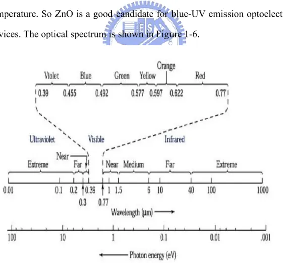
The strong exciton binding energy of ZnO (~60 meV) is larger than that of ZnSe (~22 meV), GaN (~25 meV), and the thermal energy of ZnO (~26 meV) which are favorable for obtaining an efficient excitonic laser action at room temperature. So ZnO is a good candidate for blue-UV emission optoelectronic devices. The optical spectrum is shown in Figure 1-6.
Zinc oxide generally had two kinds of emission manner. One is the ultraviolet emission (UV emission), and the other is the visible emission. The UV emission is related to the conduction band and valence band of zinc oxide. The mechanism of the emission is shown in Figure 1-8. The visible emission was related that the electron transition from valence band to the energy bands of impurities and defects. The characterization of ZnO emission changes when the component, structure and defects change.
The visible emission 30 originates from the oxygen vacancies according to the research of Vanheusden et al.31. By full-potential linear muffin-tin orbital method, the visible emission of ZnO is because that the oxygen interstitials (Oi)
occupy the zinc vacancies (VZn) to form the defect of antisite oxide (OZn). The
kind of defect is easily formed because the antisite oxide has relatively low formation energy. It is shown in Figure 1-7. All prepared films are n-type and the majority donors are oxygen vacancies (VO) and zinc interstitials (Zni). It is
proved that the singly ionized oxygen vacancy is responsible for the visible emission and this emission results from the recombination of a photogenerated hole with a singly ionized charge state of this defect. As singly ionized oxygen vacancies increases, the stronger the luminescence intensity increases, too32.
Figure 1-8 shows the mechanism of the photoluminescence. The excitation of zinc oxide (ZnO) is the photon excites the electrons from valence band to excited state. And use the combination of electrons and holes to release the photon, heat or another form of energy. The exciting energy which was higher than the energy level of ZnO make the electrons of the sample absorb the illuminant energy and then jump to higher level. After that it would spontaneously jump to the low level. And then release the energy in the form of light. When there exists another energy state between excited state and the
valence band, for example: donor level or accepter level. The excited form was from the valence band to the excited state and then from the excited state to donor level or accepter level and the last to the valence band. The form would make the FWHM value increase. Besides, as the carrier concentration increases, the excited state would approach the conduction band. At last, it would form the degeneration phenomenon. The luminescence efficiency of the compound may be inversely proportional to the number of the defect. When the electron is excited to the excited state , if have too many defects between the excited state and the valence band , the electron is easy to be absorbed in the defect , the part electrons can not combine with the holes in the valence band . So they make luminescence efficiency reduce and influence the power of intensity.
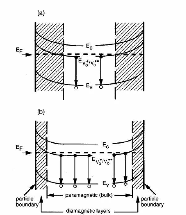
Oxygen vacancies in ZnO can occur in three different charge states: the VΦ
state which has captured two electrons and is neutral relative to the lattice, the singly ionized VO • state, and the VO • • state which did not trap any electron and is
doubly positively charged with respect to the lattice. The VΦ state is assumed to
be a very shallow donor33. The description is shown in Figure 1-9.
Ec
Ev
Eex
Eg
Ed
Photon or heat
: electron
: hole
Figure 1-9 the energy-band diagram of a ZnO grain in cross section. The conduction band (Ec), valance band (Ev), Fermi level (EF), paramagnetic
oxygen vacancy (VO•) level, and the diamagnetic VO• • area (hatched) in the
grain-boundary depletion region are visualized for a grain with a (a) low and (b) high free-carrier density.
1.3.2 Field Emission
Field emission is a point discharge phenomenon. It is occurred at high aspect ratio structure. The tip of structure exhibits electric field when we apply large field. At the same time, the potential barrier would narrow and electrons at the Fermi level could tunnel through the narrow barrier. The high aspect ratio and sharp tip structures like nanowires, nanotubes and nanorods are suitable for cold cathode field emission application. When we applied a negative voltage on nanowires, the negative voltage would induce a high electric field on the tip of structures. The high electric field will let the potential barrier narrow as the Figure 1-10. If the potential barrier is narrow enough, electrons would pass through the barrier as result in the current.
Figure 1-10 the tunneling phenomenon
This phenomenon is Fowler-Nordheim tunneling. This phenomenon is highly dependent on both the properties of the material and the shape of the particular cathode, so that higher aspect ratios produce higher field emission currents. This field emission current density can be described by the F-N equation. The F-N equation is as follow:
3 2 2 2
exp[
]
J
β
β
Α Ε
ΒΦ
=
−
Φ
Ε
[1-1] 10 2 1.56 10 (− AV eV− ) Α = × [1-2] 3 3 26.83 10 (
eV V um
−)
Β =
×
[1-3] Where J is the current density, E is the applied electric field of tip, is the work function (eV), β is the field emission enhancement factor, A and B are canstants. The logarithmic form of Eq. [1-1] can be expressed as follow:Φ 3 2 2 2 1 ln( J ) ln( β ) β ΒΦ Α = − + Ε Ε Φ [1-4]
A plot of log(J/E2) versus 1/E will be a straight line with slop m and intercept b. Slop m and intercept b is gived by follow:
3 2
m
β
ΒΦ
= −
[1-5] 2ln(
)
b
=
Α
β
Φ
[1-6] 1.3.3 Gas SensingThere is a long history for use ZnO as a gas sensing material. The development of wide bandgap semiconductor gas sensors for applications was including detection of combustion gases for fuel leak detection in spacecraft, automobiles and aircraft, fire detectors, exhaust diagnosis and emissions. Wide bandgap semiconductors such as ZnO are capable of operating at much higher temperatures than more conventional semiconductors such as Si. The ZnO diode or field-effect transistor structures are sensitive to gases such as hydrogen
and hydrocarbons. Idealsensors have the ability to discriminate between different gases and arrays that contain different metalox ides (e.g. SnO2, ZnO,
CuO, WO3) on the same chip can be used to obtain this result. The gas sensing
mechanism suggested include the desorption of adsorbed surface oxygen and grain boundaries in poly-ZnO, exchange of charges between adsorbed gas species and the ZnO surface leading to changes in depletion depth and changes in surface or grain boundary conduction by gas adsorption/desorption.
Chapter 2
Experimental
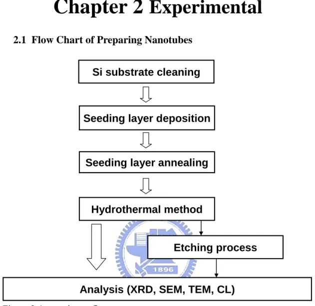
2.1 Flow Chart of Preparing Nanotubes
Etching process
Analysis (XRD, SEM, TEM, CL)
Si substrate cleaning
Seeding layer annealing
Seeding layer deposition
Hydrothermal method
2.2 The Process of Nanotubes
ZnO nanotubes were synthesized on p-type Si substrate by acidic etching ZnO nanowires. The experimental was divided to two steps. The first was fabrication of ZnO nanowires and the other one was etching process of ZnO nanaowires.
2.2.1 Preparation of Nanowires
As-prepared procedure was standard RCA clean for p-type Si substrate. It is known that ZnO nanowires is hard to grow on Si substrate because the lattice constants are mismatch. So we should coat the seeding layer to improve the growth rate. The cleaned substrate was deposited ZnO seeding layer by radio frequency (RF) sputtering (30W at 10-2 torr for 30 min). The thickness of seeding layer was about 70nm. Then the substrate with coating ZnO layer was annealed for improving the (002) face of ZnO layer. The improvement of (002) face is related to annealing temperature. Generally, the crystal quality is as strong as the temperature rise. But ZnO melts when the temperature exceeds 900。
C. The (002) face is the strongest when the temperature is about 700-800。
C. The substrate was kept in O2 ambient for 3 h at 750。C. Figure 2-2 shows the Si
substrate with ZnO seeding layer.
p-type Si substrate
ZnO seeding layer
p-type Si substrate
ZnO seeding layer
After the thermal process, the substrate with ZnO layer was grown nanowires by hydrothermal method. The chemical solution is mixed 75ml zinc nitrate hexahydrate solution and 75ml hexamethylenetetramine solution in a vessel at 95 for 2 hours. The concentrations of two solutions were 0.025M and 0.05M for different diameters. The substrate with nanowires was obtained after cleaning the substrate by dipping DI water and drying in air. Figure 2-3 is a chart of the structure.
p-type Si substrate
ZnO nanowires
p-type Si substrate
ZnO nanowires
Figure 2-3 The Si substrate with ZnO nanowires
2.2.2 Etching Process
It is known that ZnO dissolute in strong acid and alkali solution. But it is chemical stable in weak alkali solution. The weak acid is chosen to etching the nanowires due to it is safer and easier to be got than strong acid and alkali. Beside this, there is a research that the etching ZnO surface behavior between acetic and hydrochloric acids34. In the study, the diluted acetic acid is better than diluted HCl due to the selectivity is better. The etching process is anisotropic due the (002) face is polar face.
acid concentration is an important point of etching process. It is related to selectivity. In first etching experiment, a default concentration
(Vacetic:Vwater=1:10000) was set and the reaction was kept for 20 min~18 h at
85。
C. The nanostructures were gotten after the substrate dipped DI water and dry in air. In second, we modified the concentration and observed the etching process and result. Figure 2-4 is the chart of the process.
In some experiments, we changed the acidic concentration to observe the difference of etching process. The experiments helped us to establish etching model and understand the etching process.
Acidic etching Acidic etching
Figure 2-4 ZnO nanotube synthesized by acidic etching nanowire
2.2.3 Annealing
Generally, annealing process improves the sample structure, crystal quality, and repair defect. Annealing of ZnO nanowires is widely researched for improve the light emitter. ZnO nanowires after annealing reduce surface states, improve (002) face and other faces so that the UV intensity is improved and visible light intensity is reduced in PL and CL spectra. It is expected that the annealing process could improve crystal face except (002) face result in the
selectivity is better, so sample was annealed for improving crystal quality. The substrate with nanowires was annealed before etching process. It is put in quasi tube for 30 min in N2 or O2 ambient at 300~900。C. It is expected
that the nanowires structure is stronger than that before annealing and the hexagonal structure is not damaged in lower temperature.
2.3 The Experimental Equipment
2.3.1 System of Radio Frequency Magnetron Sputter
Sputtering system has been widely used to deposit various metal films in ULSI process, and it was also used to deposit dielectrics because of its easy-control and low cost. The sputtering system is composed of several parts including
(a) Mechanical modules: vacuum chamber, targets, and shutter. In addition, the rotational substrate holder was controlled by a DC motor to let the thin films grow uniformly.
(b) Vacuum pump modules: one diffusion pump (high vacuum pump) and one mechanical pump (low vacuum pump). The chamber base pressure was evacuated to 2 x 10⁻⁵ torr prior to the thin film deposition.
(c) RF power modules: the RF power generator (13.56 MHz) was controlled by a RF power supply with an automatic matching network, which can be tuned to minimum reflected power.
(d) Pressure modules: pressure gauge, exhaust valves, gas supply, and mass flow controllers. Pure gas was introduced by mass flow controllers after the system was evacuated to base pressure. The working pressure is controlled by pressure modules and vacuum pump modules.
2.4 The Measured Equipment
2.4.1 Scanning Electron Microscopy
The surface structural and morphology analysis of the ZnO nanowires and the Al-doped ZnO nanowires was observed by field emission scanning electron microscopy (FE-SEM, Hitachi S-4700I). The measured pressure was at 2 x 10⁻⁶ Torr. The working voltage was 15 keV. The working current was 10μA.
2.4.2 Transmission Electron Microscopy
The structure and morphology analysis of ZnO nanowires and nanotubes was measured by the high resolution transmission electron microscopy (HR-TEM, JEOL JEM-2010F). The TEM is the equipment which produces the diffractive and scattering electrons by the interaction between substances and electrons. According to the selected area electron diffraction (SAED), it shows the crystalline structure of the ZnO nanowires, The HR-TEM shows that the lattice constants of the ZnO nanowires. In order to measure the other elements resided on ZnO nanotubes, the EDX of the TEM is used. The fixed quantity analysis of the EDX is also used for the quantity of Zn and O.
The preparation of the TEM samples is put in the ultrasonic vibration. The rate of the vibration is about 14000 rpm. The vibration time is 3~5 minutes. And then put it on the copper ring.
2.4.3 Cathodluminescence
The optical properties are measured by the Cathodluminescence spectrum (CL, JEOL JSM6500F) with an electron beam as an excitation source (15 KV) at room temperature. Cathodluminescence was a kind of non-subversive optical measurement. By the analysis of Cathodluminescence (CL) spectrum, it can measure the band gap of solid materials and devices, and the defects and impurity of the materials. Different materials had different excitation source. When the light illuminates the sample, the photon energy makes the electron of atom jump from ground state to excited state. Because the excited state was very unstable, the electron would subsequently jump to ground state. Between the transitions of electron, the redundant energy would release in the form of heat energy or photon energy. The released energy was called the photoluminescence.
The Cathodluminescence spectrum is mainly used for measuring the optical spectrum. The excitation source is 15 KV. And the value of the photomultiplier tube (PMT) is -800V. The sweeping range is from 350nm to 700nm. The sweeping rate was 2nm per second.
2.4.4 X-ray Diffraction
The crystal structure of the ZnO nanowires and the Al-doped ZnO nanowires was observed by the X-ray diffraction (XRD, Bede, D1). X-ray diffraction (XRD) was the equipment most used for identifying the crystal structure. If the included angle θ (Bragg`s angle) between the crystal plane and the incident light matched the Bragg`s law (nλ=2dsinθ), the incident light was
diffracted by the crystal plane. By using Bragg`s law for diffraction, the reflected x-rays from the respective atomic planes can be measured by the detector. In the Bragg`s law (nλ=2dsinθ), nλ is an integral number of wavelengths, and d is the distance between two successive crystal planes.
The X-ray diffraction measurement with Cu Kα radiation (λ=1.5418 Å) was operated at 30KV and 20mA. In order to avoid the peak of silicon at about 70°, the angle 2θ of the measurement was from 30° to 60°. The sweeping rate was 4° per minute.
Chapter 3
Results and Discussion
3.1 The Preparation before Etching Process
Although we should take notices on nanotubes structure in the experiment, the nanotubes is synthesized by etching nanowires. The characteristics of the nanowires are also important for etching process. It effected directly the fabrication of ZnO nanotubes. At first, we introduced the properties and characteristics of ZnO nanowires. According to them, the etching mechanism of the ZnO nanotubes synthesized by acidic etching nanowires was understood clearly.
3.1.1 The Characteristics of ZnO Seeding Layer
Before the nanowires growth, the ZnO seeding layer is deposited on Si substrate. The thickness of ZnO seeding layer deposited by RF sputtering is about 60 nm and is enough to offer seeds for ZnO nanowires growth. The crystal of ZnO seeding layer is dominant (002) orientation. The orientation accords with ZnO nanowires growth orientation so that the seeding layer can improve (002) orientation growth. However, the seeding layer grown by sputtering is amorphous. A high temperature annealing process is needed to improve the crystal quality of the seeding layer. The annealing temperature kept 750。
C and annealing time was 3 h. Figure 3-1 shows the SEM images of the ZnO seeding layer after annealing. It is clearly observed the thickness. Figure 3-2 shows the XRD pattern of ZnO seeding layer after and before annealing. It is observed the structure of seeding layer is improved after
annealing.
Figure 3-1 (a) the top view and (b) cross section images of ZnO seeding layer
20 30 40 50 60 In te n s ity ( a .u .) 2 theta (deg) (002) annealed as deposited
Figure 3-2 ZnO seeding layer before and after annealing process
3.1.2 The Characteristics of ZnO Nanowires
After preparation of seeding layer, the ZnO nanowires are grown on the prepared substrate by hydrothermal method. The diameter and length of ZnO
nanowires fabricated by hydrothermal method were mainly related to the two parameters: growth time and reactant concentration. As the growth time and reactant concentration increase, the diameter, length, and density of ZnO nanowires increase but the variation of them also increases.
SEM Analyses
As introduction of ZnO nanowires growth at Chap. 2, the substrate was put in chemical solution. The solution was mixed by zinc nitrate hexahydrate ( Zn(NO3)2.6H2O (99.9% purity) ) and hexamethylenetetramine (HMTA,
C6H12N4 (99.9% purity) ). The chemical solution mixed with the ratio of 1:1.
For controlling the diameter and density of ZnO nanowires, the concentration of mixed solution was 0.0125M, 0.025M, and 0.05M and the growth time was fixed to 2 h. The diameter and density obviously increased as the concentration increased. And the variation of diameter increased, too. It is as the phenomenon many researchers reported. The diameters of 0.0125 M, 0.025 M, and 0.05 M were about 80-120, 100-200, 100-250 nm. The control of diameter and density is an important point when etching nanowires. This topic will be discussed at next section. The length of them is about 1-2 μm and enough to be etched.
After nanowires growth, some substrates were annealed. We separated the annealing to two parts: low temperature and high temperate. The low temperature part means the annealing temperature would not damage the ZnO hexagonal structure and the high temperature part would. The high temperature part only included two temperatures: 750。
C and 900。
C. The oxygen is selected as annealing ambient to void out-diffusion of O element. Figure 3-3 is the SEM images of high resolution and low resolution. It was clearly observed that ZnO hexagonal structure was damaged due to the temperature. There were some
differences from each other. The nanowires annealed at 750。
C only melts at corners and the hexagonal structure was damaged only on the edgy of ZnO nanowires. But the ZnO structure melts completely and merges with each other at 900。
C due to the hexagonal structure on this substrate was damaged too much.
Low temperature parts included 300。
C, 500。
C and 700。
C but adds a gas: N2 as annealing ambient. Figure is the SEM image of ZnO nanowires annealed
in O2 and N2 ambient at 500。C and 700。C. We can not observe any different
between each other from SEM images. The annealing temperature and ambient did not change the hexagonal structure in morphology so that there are no differences between each other.
(a)
(c)
(b)
(d)
Figure 3-3 low resolution SEM images of ZnO nanowires annealed at (a) 900。
C and (b) 750。
(a) (b)
(c) (d)
Figure 3-4 SEM images of ZnO annealed nanowires (a) O2, 500。C (b) O2, 700。
C (c) N2, 500。C (d) N2, 700。C
X-ray Diffraction
Figure 3-5 is XRD pattern of nanowires before annealing. The (002) peak was the strongest due to it is the orientation of ZnO nanowires growth. The peaks of other faces are very weak. The lattice constant calculated by XRD pattern match ZnO hexagonal structure. It proved the ZnO nanowire was hexagonal structure. Figure 3-6 and Figure 3-7 showed the structure of ZnO annealed in O2 and N2 ambient. It observed the structure did not change after annealing.
But the intensity of annealed sample was stronger. It meant the structure was stronger and crystal quality was better after thermal process. In this two pattern, the intensity of annealed nanowires at 700。
C is lower than that of it at 500。
C and 300。
C. It may the structure is damaged in high temperature slightly and it is observed it from SEM images.
20 30 40 50 60 (101) In te nsi ty (a.u.) 2 theta (deg) ZnO nanowires (002) (100)
20 30 40 50 60 As grown 500?C 300?C In tens ity (a.u.) 2 theta (deg) 700?C
20 30 40 50 60 300?C 500?C 700?C In te n s ity ( a .u ) 2 theta (deg) As grown
Figure 3-7 XRD patterns of ZnO nanowires after annealing in N2 ambient
Cathodluminescence spectra
Figure 3-8 shows the cathodluminescence (CL) spectra of the ZnO nanowires. The peak of UV was at about 376 nm. The band gap was 3.30 eV. The value is different from the ZnO band gap was 3.37 eV. The 3.37 eV was the band gap between the valence band and the conduction band and the 3.30 eV was the band gap between the valence band and the excited state. The cathodluminescence (CL) mainly measured the signal from the valence band to the excited state.
After the ZnO nanowires grew by hydrothermal process, the surface of the ZnO nanowires was very unstable and had a lot of dangling bond and defect due to the process was low-temperature. The dangling bond of ZnO surface tends to adsorb the steam and the impurities in the air to passivate the surface
of the ZnO nanowires to decrease surface energy. And the steam and the impurities in the air adsorbed on the surface of the ZnO nanowires were called the surface defects. The defects of the ZnO nanowires have two kinds: the radiative defects and the nonradiative defects. The radiative defects were VO,
Zni, VZn, Oi, and OZn. The nonradiative defects were the surface defects, the
lattice defects and etc. And the cathodluminescence (CL) can detect signal included the surface state and the lattice defects. The steam and the impurities in the air may decrease the UV peak and increase the luminescence intensity.
From Figure 3-8, it can find that the signal of the UV peak and visible light were near. It means that the defects in the ZnO nanowires are very much. Figure 1-7 indicated the energy of defects of ZnO nanowires. The main peak of the visible light region is at about 575 nm (2.16 eV). By the Figure 1-7, the deep-level emission is caused by the energy interval between the VO level (1.62
1.5 2.0 2.5 3.0 3.5 0 5000 10000 15000 20000 25000 30000 35000 In ten s it y (a .u .) Energy (eV)
Figure 3-8 CL spectrum of ZnO nanowires
Figure 3-9 was the CL spectrum of nanowires after annealing in oxygen atmosphere for 30 min. Although the intensity of UV and visible light peaks was reduced, the IUV/IV increased. The defect of the nanowires was reduced and
repaired because visible light peak reduced. The peak of visible light was shifted from 2.28 eV to 2 eV. It meant that the number of Oi reduced and
oxygen ions repaired the oxygen vacancies after thermal process. The energy level of 2 eV was between the VO level and Oi level. The results were similar in
N2 atmosphere just IUV still increased after annealing. It maybe the surface of
ZnO nanowires absorb oxygen atom or ion but not to absorb nitrogen atom. The surface absorption reduced the IUV.
Figure 3-9 CL spectra of ZnO annealed nanowires in O2 ambient
3.2 The Characteristics of the ZnO Nanotubes
Acidic etching is a method that generally used in many industry fabrications such as microelectronic, chemical industry, and VLSI process. The mask and lithography technology is used for anisotropic etching. In the section, anisotropic etching only depended on material structure.
3.2.1 The Influence of Parameters and Scanning Electron
Microscopy Analyses Etching Time
First, the concentration of etching solution (Vacetic:Vwater = 1:10000) was
fixed as default solution and modified the etching time to observe the change of nanowire morphology. Figure 3-11 is the SEM images of ZnO nanowires etched below 1 h. The top face of ZnO nanowires was flat when etching process start (Figure 3-11(a)). It was observed that the top face was etched when the etching time is 5 min. The etching process initially started at six corners of top face of ZnO nanowire. According to previous report, the six corners had sharp morphology and high surface energy. The phenomenon is different from the nanotubes synthesized by aging35 (Figure 3-14). The aging process started at the center of nanowires. It may be related to the reaction solution. The aging process still grew along edge of nanotubes when the nanotubes were formed. After etching for 20 min, the six corners of nanowires were etched and reserved a tip at center of (002) face.
But when etching for 40 min, the (002) face was etched faster than six corners and the hollow structure was formed (Figure 3-11(e)). It was still
observed some nanowires with a tip like above mention. Figure 3-12 is the SEM images of nanowires etched for 10 h. The structure had a shallow tube structure at 1 h but as etching time increased, the depth of the nanotube increased. After 6 h, the depth of ZnO nanotubes was not measured from SEM images due to the depth of focus of FESEM was not enough to observe. However, the depth of nanotubes did not change a lot after etching for 15 h. We attributed the phenomenon to the insufficiency of reactant in solution. The anisotropic etching was related to the selectivity. The insufficiency of reactant may abate the selectivity so that the etching process stopped to deepen nanotubes. The acidic concentration of etching solution will be discussed in the next section.
The (100) face was etched in this etching process. The (100) face still looked smooth as unetched nanowires. It means the (100) face is very stable and do not react with acid in this concentration. The (002) face played main etched role due to the (002) face was polar face and had a lot of dangling bond. The concentration is suitable for etching ZnO nanowires.
However, it was not known why there were two steps in this etching process. The corners of nanotubes were first etched but (002) face was etched after 40 min. It may be attributed to the decrease of acid reactants and structures. The nanotubes may be fabricated in lower concentration.
(a)
(c)
(e)
(d)
(b)
(f)
Figure 3-11 SEM images of ZnO nanostructures after etching for (a) 5min (b) 10min (c) 20 min (d) 40 min (e) 1 h
(c) (a)
(d) (b)
Figure 3-12 SEM images of ZnO nanostructures after etching for (a) 2 h (b) 4 h (c) 6h (d) 10 h
(c)
(b)
(a)
(c)
(b)
(a)
Figure 3-13 SEM images of ZnO nanostructures after etching for (a) 12 h (b) 15 h (c) 17 h
Acid Concentration
The ZnO is dissoluble in the strong acid and alkali solution. Although weak acid was used to etching ZnO nanowire for nanotube, we should control acid concentration to void etching (100) face and to improve selectivity. We also want to prove the change of etching process is not related to acidic concentration. In this section, we will research the effect of acid concentration and etching process.
First, we want to know whether the lower concentration of acid is the key point of change of etching process. The lower concentration (lower than default concentration) was used and fixed etching time (1 h and 12 h). The accurate concentrations were Vacetic:Vwater = 1:100000 (A), 1:40000 (B), 1:20000 (C),
and 3:40000 (D). Figure 3-15 is the SEM images of nanowires etched in above solutions for 1 h. We can see that the nanowires were nearly not etched in sample A and B. It means the solution is too weak to acidic etch ZnO nanowires. The top of nanowires of sample C was like the nanowires etched by default solution for 20 min and had a tip on (002) face. The nanostructure of sample D looked like the tube structure, but it is still very shallower than nanotubes etched by default solution for 40 min. We also etched nanowires for 12 h by the same four solutions. Figure 3-16 shows SEM images of them. The nanowires were still not etched in the lowest solution. We concluded that ZnO nanowire is very stable in low concentration acetic acid and pure water. It means the relation of etching rate and reactant concentration is not linear. The depths of the nanotubes of sample C and D were 20~40 nm and 100~200 nm. In this experiment, we saw the nanotubes on sample D after etching for 1 h. If the acidic concentration changed the etching process, the lower concentration acid should form nanotubes. However, only higher concentration acid
synthesized nantubes. It means the change of etching process is not relation to acidic concentration.
Next, we want to know the acidic resistances of other faces and would discuss the higher concentration. However, we can not set the etching time corresponding to that of lower concentration and even set different time between two higher concentrations due to etching rate is too fast. The ZnO nanostructure and ZnO seeding layer can not bear so high etching rate.
Continue increase the concentration of etching solution but reduce the reaction time. We tried the higher concentration of solution (Vacetic:Vwater=
1:1000, 1:100, and 1:10) as etching solution and the reaction time is 500s, 50s, and 10s. Figure 3-17 is the SEM images. In this experiment, the tube structure was not synthesized. But the nanostructures are different between them. The six corners played mainly etched role in the lowest solution so that the nanotube structure was not synthesized. The top of nanostructure looked like a hexagram. The (100) face was not etched directly but it still was etched along six corners. The etching process only occurred on the top of nanowires. We did not see the middle of the nanowires was etched. The nanowires looked smooth expect the top of nanowires. It means the other faces expect (002) face and six corners is stable even the nanotubes is not formed due to the etching rate of six corners is too fast. However, we observed the (100) face etched directly on the substrate in the next solution (1:100, 50s). The nanowires were etched form all orientations due all faces of ZnO nanowires were damaged. The nanowires solved in the next concentration (1:10, 10s).
(a)
(c)
(b)
(d)
Figure 3-15 SEM images of ZnO nanostructure etched for 1h in (a) 1:100000 (b) 1:40000 (c) 1:20000 (d) 3:40000 solution
(a)
(d) (c)
(b)
Figure 3-16 SEM images of ZnO nanostructure etched for 12h in (a) 1:100000 (b) 1:40000 (c) 1:20000 (d) 3:40000 solution
(a)
(c)
(b)
Figure 3-17 the SEM images of ZnO nanowires etched in (a) 1:1000, 500s (b) 1:100, 50s (c) 1:10, 10s solutions
Diameter of Nanowires
The diameter of nanowires depends on the concentration of growth solution as above mention. We control growth solution and etching nanowires by default etching solution. Figure 3-18 is their SEM images. We tried to etch nanowires synthesized by 0.05M, 0.025M, and 0.0125M solutions. The nanotubes structure was fabricated in the first and second experiments. But we did not explore nanotubes even nanowires in the last experiment due the seeding layer was removed. The diameter of the last sample is about 80-100 nm. It may mean the process is only suitable for the diameter of nanowire larger than 100 nm. However, we discovered nanotubes have such diameter on other sample grown in higher concentration solution despite very shallow tube. There were other reasons so that the nanowires of 0.0125M solution did not synthesize nanotubes. The possible reasons was the density of nanowires was too low and the surface of (002) face was too less so that the acid reactant was not react with ZnO nanowires completely but some with ZnO seeding layer result in seeding layer was removed.
(a)
(c)
(b)
Figure 3-18 the different diameter (a) 0.05M (b) 0.025M (c) 0.0125M nanowires etched for 12 h
Annealed Nanowires
The nanowire after annealing improves the crystal quality and reduces the defects and surface states. We divided two parts to discuss this parameter: low temperature and high temperature. The low temperature part means the annealing would not damage the ZnO hexagonal structure. But the high temperature part damaged the hexagonal structure. To damage the hexagonal structure by high temperature annealing is for proving that the mechanism of the nanotube is attributed to hexagonal structure.
The morphology of nanowires was observed after temperature annealing in Figure 3-19. The corners of the nanowires annealed at 750。
C rounded and the structures at the round corners were not hexagonal. The nanowires annealed at 900。
C melted and adhered to each other. After default etching process, the nanowires annealed at 750。
C were only etched at the edgy of top face and (100) face. The (002) face was stable in this experiment. The possible reason is the round corners is weaker than (002) face due to the corners were not hexagonal structure but other structure. Their bonding energies were weak so that they tend to be etched and decreased the concentration to prevent the (002) face from be etched. Temperature increases up to 900。
C, the nanowires melted and had no rule. It proved the hexagonal structure is the important point in this fabrication.
The nanotubes can be synthesized by acidic etching nanowires due to (002) face is polar face in hexagonal structure. In ideal case, it is stronger but still weaker than other faces and tends to react after annealing. The annealing may increase the selectivity of etching process. We did not observe any different from original sample (Figure 3-4). However, the nanowires did not synthesize nanotubes after etching (Figure 3-19). The edge of (002) face of
nanowires annealed at 300。
C and 500。
C was etched and some wires became a tip. The sample annealed at 700。
C looked like the nanostructure annealed 750。
C. The edge of top face and six corners were etched but the damage was less at six corners due to the structures of six corners were damaged much after annealing at 750。
C. The samples were also annealed in N2 ambient (Figure
3-21). The result is the same as that in O2 ambient. There were no nanotubes on
the substrate.
(a)
(d)
(c)
(b)
(a)
(d)
(c)
(b)
(a)
(d)
(c)
(b)
Figure 3-19 SEM images of nanowires annealed at (a) 750。
C and (b) 900。
C, (c) and (d) were etched in default solution for 12 h
(a)
(c)
(b)
(a)
(c)
(b)
Figure 3-20 SEM images of etched for 12 h, nanowires annealed at (a) 300。
C (b) 500。
C (c) 700。
(a)
(c)
(b)
(a)
(c)
(b)
Figure 3-21 SEM images of etched for 12 h, nanowires annealed at (a) 300。
C (b) 500。
C (c) 700。
3.2.2 Transmission Electron Microscopy Analyses
Figure 3-22 is the TEM images of nanotubes etched for 12 h in default etching solution. The diameters of them were 300 nm and 100 nm. The nanotubes with different diameters were got from the same sample. We observed clearly the depths of the two nanotubes were about 500 nm. The bottom of nanotubes was smooth and it proved the etched face was exactly (002) plane. It indicated that this etching process is uniform. The SAED pattern and HRTEM images showed the hollow region of the nanotubes was still single crystal after etching. The nanowires structure was not damaged in this process.
Figure 3-23 shows the TEM images of nanotubes with different diameter. We got the two nanotubes on the same sample. It was clearly observed that the two nanotubes has nearly same depth: 500nm. However, the diameter of Figure 3-23 (a) is about 300nm and it of Figure 3-23 (b) is only 100nm. It means the etching process have uniform etching rate on different diameter nanowires.
5nm 002 100 102 002 100 102 200 nm
(a)
(b)
Figure 3-22 (a) TEM image of ZnO nanotubes (b) HRTEM image of hollow region, the inset is SAED pattern
(a)
(b)
200 nm
(a)
(a)(b)
200 nm
(a)
Figure 3-23 the TEM images of different diameters of ZnO (a) 300 nm (b) 100 nm
3.2.3 X-Ray Diffraction
Figure 3-24 is the XRD pattern after etching for 12h. The intensity of (002) peak was still very strong due to the nanowires was not etched completely. It was just etched the top region of ZnO nanowires. But the intensity of (002) peak of nanotubes was weaker than it of nanowires. Like SAED pattern and HRTEM image, the XRD patterns also proved the hexagonal structure was not changed after etching process.
20 30 40 50 60 In tensi ty (a.u. ) 2 theta (deg) Etched for 12h As grown (002) (101) (100)
Figure 3-24 XRD patterns of nanowires before and after etching for 12 h
3.2.4 Cathodluminescence Spectra
Figure 3-25 is the room temperature CL spectrum. The intensities of UV and visible of ZnO nanowires are nearly. The peak of UV light is 3.28 eV and it is very near to exciton energy. There is a sharp slope at 3.37 eV due to it is the band gap of ZnO. The visible emission is related to surface state and structure defects. The high intensity of visible light is also proved that the nanowire is defect-rich and its structure is low crystal quality. After thermal process, the intensities of UV and visible emission are reduced. The decrease of visible light is meant that annealing process repairs oxygen defects. But the abatement of UV light is related to annealing ambient and ZnO surface state. The surface of ZnO nanostructures adsorb oxygen ion and form depletion layer.(Band
bending at the surface serves to separate the photogenerated electron-hole pairs reducing the probability of recombination, hence reducing the UV emission intensity from the surface region.) When ZnO nanowires are annealed in oxygen ambient, the surface adsorbs more oxygen ions and reduces UV emitter again. After etching process, the intensity of UV emission is stronger and the intensity of visible light is weaker than it before etching whatever annealed or unannealed nanowires. The possible reason is the oxygen ions on ZnO surface are removed by H+ ions. After reducing surface state, the depletion layer narrows and decreases the possibility of separated electron-hole pairs so enhance the efficiency of UV light and depress the intensity of visible light. However, the IUV/IV ratio of ZnO nanotubes is very stronger than it of annealed
and etched nanowires. It may be related to the structure. According to above mention, the nanowires without annealing have a lot of defects. The weaker, defect-rich structure of ZnO nanowires would be etched by acidic solution and reduce the oxygen defects so that decrease the intensity of visible light.
1.5 2.0 2.5 3.0 3.5 0 20000 40000 60000 80000 100000 120000 In te n s it y (a .u .) Energy (eV) as grown annealed etched
annealed and etched
3.3 The Discussion of Etching Model
3.3.1 The Etching Model of ZnO Nanotube
Figure 3-26 the sample chart of etching process
First, we discussed relation of the nanowires and time in etching process. The nanotubes was synthesized after complete process. The depth of nantubes was as deep as etching time increased. However, the tips of nanowires were seen at 20 min. Figure 3-26 is sample chart of etching process. It means the six corners tended to be etched at initial but the (002) face did after 40 min. It was very strange. Figure 3-27 is the structure of hexagonal ZnO. It shows that there is polar Zn on the (002) plane due the bonds of polar Zn is not enough. Why were six corners etched after etching for 40 min due to their shape morphology? Why was (002) face not etched at initial because of polar plane? It already proved the reason of change was not relate to concentration. It should be related to structure.
We assumed that etching reactant always etched the part which acidic resistance was weaker. The etching process always etched one part in lower concentration according to SEM images above mention. Six corners were etched at initial due to their acidic resistance were weaker than that of (002) face of the nanowires. But how to explain it was stronger than (002) face after 40 min. Maybe the acidic resistance of the (002) face of nanowire surface was different from that of nanowires bulk. How to explain the acidic resistance of the (002) surface is stronger than it of (002) bulk?
The (002) surface was defect-rich and polar plane so that had a lot of dangling bonds. The dangling bonds tended to absorb hydrogen iron or other iron to form OH- bond and reduce surface energy. The OH- bonds may play an important role in this etching process. ZnO dissolves in acid because the H+ ion react with ZnO. The OH- bond can reduce H+ concentration locally. It can prevent the surface ZnO from being etched.
First, we assume the etching process only etch the region which its acidic resistance is the weakest in this concentration. The assumption is like loading effect, the stronger part is not etched due to the weaker one consumed reactants quickly. The acidic resistance of six corners is the weakest on the nanowires and even weaker than the (002) face so that they are mainly etched. The nanowires were be etched along the six corners to form tip structure on the (002) plane.
According to the first hypothesis, the acidic resistance of surface (002) plane should be stronger than it of six corners and (002) plane of bulk. The possible reason causes phenomenon due to ZnO hexagonal structure and fabrication. ZnO nanowires synthesized by low temperature hydrothermal method are low crystal quality, defect-rich. Simultaneously, ZnO hexagonal
structure has a lot of dangling bonds on (002) face due to polar plane. The dangling bonds tend to absorb the OH- bonds and other ions to be more stable in air36. The acidic resistance of (002) plane with OH- bonds should be stronger and more chemical stable than that of six corners and (002) plane of bulk in acidic solution due to OH- bonds reduce the local H+ concentration and prevent the plane from be etched (Figure 3-28). The acidic resistance of six corners is stronger than (002) plane of bulk due to (002) plane is defect-rich and polar plane.
According to above discussion, the etching model is established and divided to two steps. The first step, the etching process starts at six corners due to its high surface energy. At the same time, the (002) face of surface is etched along six corners and reserves a tip on the face. When the (002) face of nanowires bulk is exposed to acidic solution after etching reaction proceed along six corners. The nanotubes is synthesized due to its acidic resistance is the weakest so that the six corners are etched slowly. This is the second etching step. When etching time was too long, the wall looked thinner and the nanotubes looked shallower due to two reasons. Although the etching process etches the wall very slowly, the wall of nanotubes is still thinner after so long reaction time. The thinner wall will accelerate the etching rate of (002) orientation of the wall. The other reason, the etching selectivity is also related to acidic concentration. When the acidic was sufficient, the (002) plane tends to be etched after the first etching step. After 15 h, the concentration is too low so that the etching rate of (002) plane is lower than other faces.
The acidic resistance plays an important role in acidic etching process. It is related to structures and bonds. One improvement is the faces of interlaced nanotubes tend to be etched in the process due to the structures of these faces
have more defect and high stress. The other improvement, the annealed nanowires at O2 or N2 ambient is still hexagonal structure. There are not any
differences between annealed and un-annealed samples in morphology. The sample was etched in the same acidic solution for 12 h, but it was never observed nanotube structure. It is known that the annealing process can enhance the crystalline37, improve crystal quality38,39, repair defect, and reduce the OH- bond on the surface. However, the OH- bonds are absorbed again after putting the sample in air so that the acidic resistance of surface (002) face is still stronger than it of six corners. The second step will not occur due to the annealing process enhances structure quality. The acidic resistance of (002) plane of nanowires bulk becomes stronger than it of six corners after annealing process. Result in the etching reaction only stayed on the first step. We also observe the nanowires only is etched the edge of (002) plane of larger diameter nanowires and the small diameter nanowires synthesizes nanopencil. The etching rate of annealed nanowires is lower than it of unannealed nanowires due to the strength of nanowires structure is enhanced. It proved the structure quality of nanowires is an important role when acidic etching process and related to acidic resistance. Figure 3-29 is a complete chart of etching model.