國
立
交
通
大
學
電子工程學系 電子研究所
博 士 論 文
具獨立雙閘極之多晶矽奈米線薄膜電晶體的研製與分析
Fabrication and Analysis of Independent Double-Gated
Poly-Si Nanowire Thin-Film Transistors
研 究 生: 陳威臣
指導教授: 林鴻志 博士
黃調元 博士
具獨立雙閘極之多晶矽奈米線薄膜電晶體的研製與分析
Fabrication and Analysis of Independent Double-Gated
Poly-Si Nanowire Thin-Film Transistors
研 究 生:陳威臣 Student:Wei-Chen Chen
指導教授:林鴻志 博士 Advisors:Dr. Horng-Chih Lin
黃調元 博士 Dr. Tiao-Yuan Huang
國 立 交 通 大 學
電子工程學系 電子研究所
博 士 論 文
A Dissertation
Submitted to Department of Electronics Engineering and Institute of Electronics
College of Electrical and Computer Engineering National Chiao Tung University
in partial Fulfillment of the Requirements for the Degree of
Doctor of Philosophy in
Electronics Engineering October 2011
Hsinchu, Taiwan, Republic of China
具獨立雙閘極之多晶矽奈米線薄膜電晶體的
研製與分析
研究生:陳威臣 指導教授: 林鴻志 博士 黃調元 博士 國立交通大學 電子工程學系 電子研究所摘要
本篇論文提出一簡易且低成本之製作多晶矽奈米線元件的方法。此法的特點 在於利用將電感耦合電漿式(inductively coupled plasma)蝕刻機台中的偏壓電源 (bias power)關閉並搭配使用六氟化硫(SF6)的氣體以得到一具等向性與高蝕刻選擇 比的蝕刻條件。將此參數用以側向蝕刻臨場摻雜多晶矽後便可形成寬度在10 奈米 ~100 奈米之向內凹陷的空隙,進而定義出奈米線的線寬。另外,當奈米線形成後, 如果再沉積上第二層的介電層與閘極材料,此元件就具有獨立雙閘極的結構,可 使元件的操作彈性大幅提升。 首先藉由控制側向蝕刻的時間,我們製備了具有不同寬度的奈米線元件,用 以探討奈米線尺寸對元件電性的影響。與兩種單閘操作模式相比,實驗發現當奈 米線越窄,在雙閘操作模式下電性改善的程度會有顯著的增加。經由量測分析, 可得知這是由於奈米線尺寸會影響多晶矽的晶界能障受閘極調控的程度所導致。 然而為了避免通道受到摻雜,原本所設計之元件製程卻會造成源/汲極的串聯電阻 過大。因此,我們提出一種改良的流程,將臨場摻雜多晶矽取代離子佈值做為形成源/汲極區的製備方法。採用此技巧所完成的元件除了具有明顯改善的導通電流 與漏電流之外,更能夠達到只有73 mV/dec 的次臨界擺幅(subthreshold swing),這 是目前文獻上多晶矽元件最佳的成果。 除了最佳化製程以改善元件特性外,為了探討奈米線載子傳輸特性,本研究 也在製程中引入電子束微影技術,進而將通道長度微縮至 100 奈米以下,同時搭 配低溫量測設備來完整分析元件導通機制。研究發現,當測量溫度低於約 100 K 時,有一單閘模式下的轉換曲線會展現出低於傳統金氧半場效電晶體(MOSFET) 極限的次臨界擺幅,而且此現象只發生在通道長度小於 100 奈米的元件。經由模 擬及實驗證實,這個效應是來自於閘極經過離子佈值後,雜質分佈不均而導致閘 極對通道的控制能力會隨通道位置改變而變化,因此沿通道方向的能帶圖會形成 一類似駝峰的曲線所致。 有鑑於近來三維記憶體技術多使用多晶矽做為主動層,本研究也討論獨立雙 閘多晶矽奈米線結構應用於矽-氧化矽-氮化矽-氧化矽-矽(SONOS)非揮發記憶體時 所衍伸的價值與各種操作上的可行性。首先,量測上發現當進行寫入/抹除時,除 了在主動閘施加一偏壓外,寫入/抹除的速度會隨輔助閘偏壓的增加而明顯加快, 其原因來自於輔助閘偏壓能夠有效的影響奈米線中的電子密度,因而影響穿隧電 子的數目與其效率。另一方面,本研究所製作的記憶體元件其雙閘極介電層材料 分別為二氧化矽與二氧化矽-氮化矽-二氧化矽,當採用具二氧化矽介電層之閘極為 讀取閘時,寫入/抹除態的感測窗口會展現出與輔助閘施加偏壓的相關性,然而此 現象並不會在傳統上以二氧化矽-氮化矽-二氧化矽為介電層之閘極做為讀取閘時 發生。研究發現其根本原因為背閘效應(back-gate effect)。於此架構下,我們做了 許多此兩種讀取模式的操作特性比較,包括寫入/抹除速度、保持性與耐操性。最 後我們嘗試將二氧化矽-氮化矽-二氧化矽同時做為雙閘極之介電層材料以驗證單 一元件具有二位元儲存(2-bit/cell)的可行性。
關鍵字: 奈米線, 獨立雙閘極,多閘,多晶矽,臨場摻雜,薄膜電晶體,次臨界 擺幅,穿隧,雜質,低溫測量,遲滯,非揮發記憶體,矽-氧化矽-氮化矽 -氧化矽-矽,背閘效應,單一記憶胞二位元儲存
Fabrication and Analysis of Independent
Double-Gated Poly-Si Nanowire Thin-Film Transistors
Student: Wei-Chen Chen Advisor: Dr. Horng-Chih Lin Dr. Tiao-Yuan Huang
Department of Electronics Engineering & Institute of Electronics National Chiao-Tung University
Abstract
A simple and low-cost method of fabricating poly-Si nanowire (NW) devices is proposed in this dissertation. The feature lies in turning off the bias power in an inductively coupled plasma etcher combined with the addition of SF6 gas to obtain an
isotropic etching recipe with high selectivity. A re-entrant 10~100 nm wide cavity inside the in situ doped poly-Si could then be formed with this recipe, which in turn determines the feature size of the NW. Following the formation of NWs, another gate stack could be deposited and patterned such that the device has two independent gates that help increase the functionality and flexibility of device operation.
To investigate the influence of the size of NW on device characteristics, NWs with varying widths were fabricated by controlling the duration of lateral etching. It is observed that as the NW gets narrower, the performance of double-gated mode would be enhanced to a larger extent compared with that of two single-gated modes. The root cause is identified to be related to the fact that the modulation rate of grain boundary barrier height of poly-Si by the gate is dependent on the NW dimension. Nevertheless,
in order to avert inadvertent channel doping, the original device process flow is designed in a way that the series resistance of the source/drain may become too significant. In this regard, we propose a modified version of process in which in situ doped poly-Si replaces ion implantation for forming the source/drain regions. Devices fabricated with this approach demonstrate evidently improved on- and off-current. What’s more, a record-breaking value of subthreshold swing as low as 73 mV/dec could be obtained.
In addition to process optimization to better the device performance, in an attempt to probe into carrier transport characteristics of NW, e-beam direct writing is adopted in our process as well to reduce the channel length below 100 nm. Meanwhile, cryogenic measurement facilities are employed to provide a comprehensive analysis on device transport behavior. It is found that as the temperature of measurement is lower than 100 K, one of the single-gated modes displays subthreshold swing that is well below the theoretical limit of MOSFET. Plus, this kind of phenomenon is only exclusive to devices with channel lengths shorter than 100 nm. With the aid of simulation and experimental verification, it is identified that this intriguing effect is caused by the non-uniform distribution of dopants introduced by ion implantation such that the controllability of gate over the channel is a function of location along the channel and the electrostatic potential of the channel would exhibit a hump-like profile.
Given that most of the state-of-the-art 3D memory technology employs poly-Si as its active layer, the merit and operational feasibility coming from the implementation of independent double-gate scheme on SONOS non-volatile memory devices are also investigated. During programming/erasing, apart from the biases applied to the active gate, experimental results indicate that the programming/erasing speed is a monotonically increasing function of the auxiliary gate bias. This may be due to the
electron density within the NW channel that the auxiliary gate helps modulate, which in turn affects the number of tunneling electrons and the programming/erasing efficiency. The device fabricated has oxide and oxide-nitride-oxide stack as dielectrics for two independent gates, respectively. The VTH window between P/E states shows a strong
dependence on the auxiliary gate bias when the gate with oxide as dielectric is used as the read gate, which is in contrast to the fairly constant VTH window observed in a
conventional mode (i.e., the read gate is with oxide-nitride-oxide as dielectric). Back-gate effect is recognized to be the major mechanism in play. To further delve into the implications, several comparisons between those two feasible read modes are made, including programming/erasing speed, retention, and endurance characteristics. Finally, proof-of-concept 2-bit/cell feature is demonstrated by utilizing oxide-nitride-oxide stack as the dielectrics for both gates.
Keywords: Nanowire, Independent Double-Gated (IDG), Multiple-Gated,
Polycrystalline Silicon (Poly-Si), In Situ Doping, Thin-Film Transistor (TFT), Subthreshold Swing (SS), Tunneling, Dopant, Low Temperature Characterization, Hysteresis, Non-Volatile Memory (NVM), Back-Gate Effect, Silicon-Oxide-Nitride-Oxide-Silicon (SONOS), 2-bit/cell
誌 謝
首先要感謝指導教授林鴻志博士與黃調元博士,兩位老師在專業領域上的知 識、對於研究的熱誠以及實事求是的精神著實是我學習的典範。林老師嚴謹的研 究態度與對問題精闢的見解讓我學習到做研究的態度與方法。黃老師學問淵博卻 淡泊名利的風骨堪稱是學術界中的一股清流,這樣的風範令人敬佩。 本論文的完成也要感謝口試委員-趙天生教授、崔秉鉞教授、蘇彬教授、李佩 雯教授、劉致為教授、楊富量主任-所給予的寶貴建議。 接著我要感謝先進元件技術實驗室的所有成員在生活與實驗上所提供的各種 協助。要感謝蘇俊榮博士帶領我進入這個領域,在我懵懂無知時仍然能夠有耐心 地且無私地分享他的經驗並詳細地帶我實地操作儀器,使我少走了許多冤妄路, 由於他對奈米線元件所打下的基礎才得以讓本篇論文的基本元件架構能順利的完 成。另外要感謝張凱翔學長過去在生活上的幫助與研究上的討論,讓我的研究生 涯增添了不少樂趣。謝謝徐行徽博士在實驗分析上所提供的建議,也由於你的協 助,讓我可以很快的融入美國的生活,也要感謝你在烹飪方面的指導,讓我更能 享受下廚的樂趣。同時要感謝同屆的同學-洪文強、李冠樟、林漢仲、劉大偉、洪 政雄、江忠祐、陳玲-過去一同修課和熬夜做實驗的情誼是無法被抹滅的。感謝曾 經一起打拼合作過的學弟妹-張佑寧、陳政建、張育嘉、陳冠宇、劉禹玲、吳俊鵬、 林歷樺、楊竣宇-謝謝你們在實驗與量測上所提供的協助與陪伴,沒有你們的貢獻, 這本論文無法完成。感謝實驗室的學長姐以及學弟-蔡子儀、林哲民、李克慧、林 政頤、郭嘉豪等-在研究上的建議和討論。 此外要感謝國家奈米元件實驗室與交大奈米中心提供一個這麼完善的研究環 境和先進的實驗儀器,使得實驗能夠順利的進行。特別要感謝國家奈米元件實驗 室的林傳丁工程師在蝕刻與SEM 上的大力幫忙、許進財工程師在電子束微影技術 上的協助,以及陳仕鴻博士針對實驗與分析上所提供的建議。也要感謝操作小姐的幫忙-趙子綾、范庭瑋、周家如、陳琇芝、李春杏、林婉貞-才讓實驗能順利且快 速地完成。同時由衷感謝奈米中心的陳明麗小姐在聚焦離子束顯微鏡(FIB)的幫助, 讓我能夠很快的掌握機台的操作要點,對試片進行分析。
另外感謝在美國 NIST 進行訪問研究期間的主管張建平博士(Dr. Charles Cheung)、SED 部門同事、CNST Nanofab 的員工與 Taylor Kerby、Brian Hung、Steve Luk,謝謝你們的陪伴和鼓勵,讓我了解到做人處事的道理也留下了許多美好的回 憶。 最後要特別感謝我的父母親:陳慶煌先生與蔡美惠女士,謝謝你們提供我一 個健全且美好的成長環境,由於你們無私的付出和鼓勵,讓我可以勇於追求自己 的夢想。感謝妹妹陳彥君小姐,雖然你常惹我生氣,但也讓我的生活多了另外一 種樂趣。 謹以此論文獻給我的師長朋友以及最敬愛的家人。 陳 威 臣 誌於風城交大 2011 年 10 月
Contents
Abstract (Chinese) ... i
Abstract (English) ... iv
Acknowledgment……….vii
Contents…. ... ix
Table Captions ... xii
Figure Captions ... xiii
Chapter 1 Introduction ... 1
1.1 Overview of Nanowire Technology ... 2
1.1.1 Top-down Approach ... 3
1.1.2 Bottom-Up Approach ... 4
1.2 Multiple-Gated Devices ... 6
1.3 Transport Behavior of Nanowire Devices ... 7
1.4 Overview of Nonvolatile Memory Technology ... 11
1.4.1 Charge Trapping SONOS Memory ... 13
1.4.2 Nanowire-Based Nonvolatile Memory ... 14
1.5 Motivation ... 15
1.6 Organization of the Dissertation ... 17
References… ... 20
Chapter 2 Double-Gated Poly-Si Thin Film Transistor with Twin
Nanowire Channels ... 31
2.1 Introduction ... 31
2.2 Experimental ... 33
2.2.1 Investigation of Selective Plasma Etching Conditions ... 34
2.2.2 Device Fabrication Process ... 36
2.2.3 Measurement Setup and Electrical Characterization Methods ... 39
2.3 Results and Discussion ... 41
2.3.1 Impacts of Double-Gated Configuration on Device Performance ... 41
2.3.2 Dependency of Performance Enhancement in Double-Gated over Single-Gated Operation on Nanowire Channel Dimension ... 44
2.4 Summary ... 50
References…. ... 53
Chapter 3 Analysis of In Situ Doped Source/Drain for Performance
Improvement of Double-Gated Poly-Si Nanowire Thin
Film Transistors ... 83
3.1 Introduction ... 83
3.2 Fabrication Process for Devices with In Situ Doped Source/Drain ... 86
3.3 Comparison of Electrical Characteristics between Devices with Implanted and In Situ Doped Source/Drain ... 87
3.4 Summary ... 94
References…. ... 96
Chapter 4 Investigations on Transport Properties of Double-Gated
Poly-Si Nanowire Transistors under Cryogenic Ambient
... 115
4.1 Introduction ... 115
4.2 Fabrication Process for Devices with Sub-100 nm Channel Length ... 118
4.3 Electrical Characteristics at Room Temperature ... 119
4.4 Electrical Characteristics at Cryogenic Ambient ... 120
4.4.1 Evolution of Transfer Curves under Different Operation Modes with Respect to Temperature ... 120
4.4.2 Model Establishment and Discussion ... 122
4.4.3 Observation of Hysteresis and Single Electron Effects ... 127
4.5 Summary ... 130
References… ... 132
Chapter 5 Analysis on the Potential of Poly-Si Nanowire Thin Film
Transistors Featuring Independent Double-Gated
Configuration for Nonvolatile Memory Applications ... 157
5.1 Introduction ... 157
5.2 Programming and Erasing Operation Principles ... 160
5.3 Merits of Independent Double-Gated Configuration in Enhancing Programming and Erasing Characteristics ... 162
5.4.2 On Programming/Erasing Efficiency ... 167 5.4.3 On Endurance Characteristics ... 170 5.4.4 On Retention Characteristics ... 174 5.5 2-Bit/Cell Feature ... 175 5.6 Summary ... 177 References… ... 180
Chapter 6 Conclusions and Future Work ... 202
6.1 Conclusions ... 202
6.2 Future Work ... 204
6.2.1 Crystallinity of Poly-Si NWs ... 204
6.2.2 Junction-Free Feature ... 205
References… ... 207
Appendix Fabrication and Characterization of a Low Temperature
Polycrystalline-Germanium Thin Film Transistor Using
Ultra High Vacuum Sputtering ... 208
A.1 Introduction ... 208
A.2 Material Analysis of the Ge Film ... 210
A.3 Electrical Characteristics of a Poly-Ge TFT ... 213
A.4 Conclusions and Future Work ... 217
A.4.1 Conclusions ... 217 A.4.2 Future Work ... 218 A.5 Acknowledgment ... 222 References… ... 224
Vita……….. ... 235
Publication List ... 236
Table Captions
Chapter 1
Table 1-I Comparison of selected NW transistors with sub-20 nm channel length. ... 30
Chapter 2
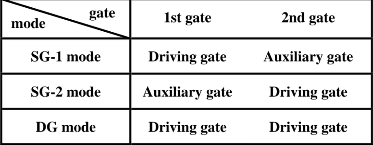
Table 2-I Definition of operation modes in I-V characterization. ... 57
Chapter 3
Table 3-I Summary of the major characteristics of devices with implanted (Fig. 3-3) and in situ doped S/D (Fig. 3-4). ... 98
Appendix
Table A-I Comparison of major device parameters among Ge-on-insulator devices. Only those not from commercial vendors are listed. ... 227
Figure Captions
Chapter 2
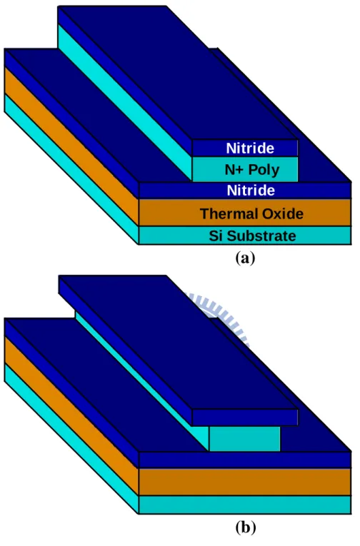
Fig. 2-1 Test structure used for investigating selective plasma-etching conditions. ... 58 Fig. 2-2 Cross-sectional SEM images after plasma etching with different conditions.
(a) The gate stack is anisotropically etched with the condition of P = 12 mtorr, Cl2 = 35 sccm, HBr = 125 sccm, top power = 310 W, bottom power = 120 W,
time = 31 sec. (b) In the aftermath of (a) step, the wafer is further subject to another etching step with the condition of P = 5 mtorr, SF6 = 20 sccm, top
power = 700 W, time = 30 sec. (Continued) ... 59 Fig. 2-2 Cross-sectional SEM images after plasma etching with different conditions.
In the aftermath of (a) step, the wafer is further subject to (c) P = 5 mtorr, Cl2
= 100 sccm, SF6 = 20 sccm, top power = 700 W, time = 20 sec, and (d) P = 5
mtorr, Cl2 = 100 sccm, SF6 = 20 sccm, top power = 700 W, time = 6 sec.
Isotropic etching component is seen to be enhanced by the addition of SF6
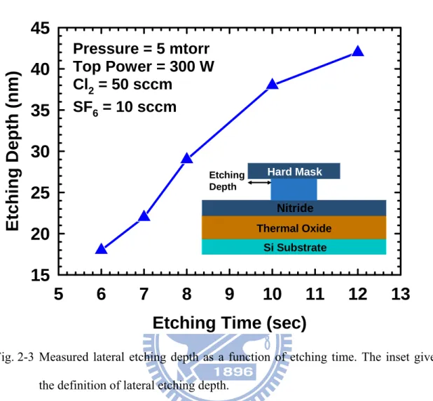
gas……….………..60 Fig. 2-3 Measured lateral etching depth as a function of etching time. The inset gives
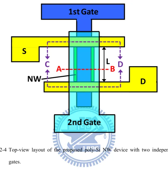
the definition of lateral etching depth. ... 61 Fig. 2-4 Top-view layout of the proposed poly-Si NW device with two independent
gates…… ... 62 Fig. 2-5 Schematic process flow for the double-gated poly-Si NW TFT (viewed along line A-B in Fig. 2-4). (a) Sequential deposition of 100-nm thermal oxide, 50-nm nitride, 100-nm in situ doped N+ poly-Si, and 50-nm nitride on a 6-in Si wafer. First gate patterning was then performed. (b) Selective plasma etching of the first gate. (Continued) ... 63 Fig. 2-5 (c) First gate dielectric (20-nm TEOS oxide) and 100-nm amorphous-Si layer deposition followed by SPC. (d) S/D implantation by phosphorous with 15 keV energy and 5 × 1015 cm-2 dosage. (Continued).………...………64 Fig. 2-5 (e) Simultaneous definition of NW channels and S/D regions using dry
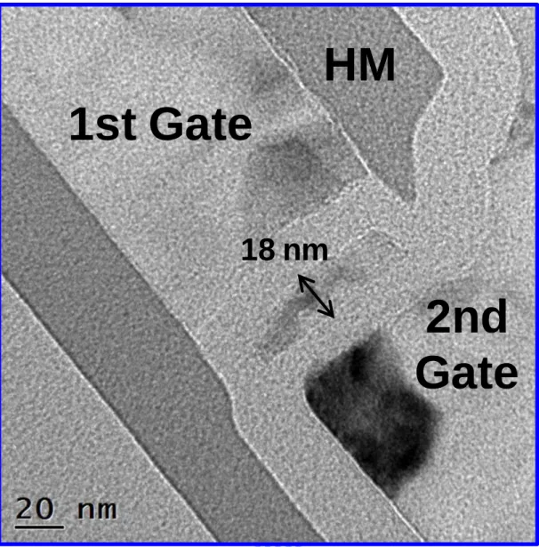
etching. (f) Second gate stack (20-nm TEOS oxide and 100-nm in situ doped N+ poly-Si) deposition and patterning………65 Fig. 2-6 Cross-sectional TEM image (along line A-B in Fig. 2-4) of an independent
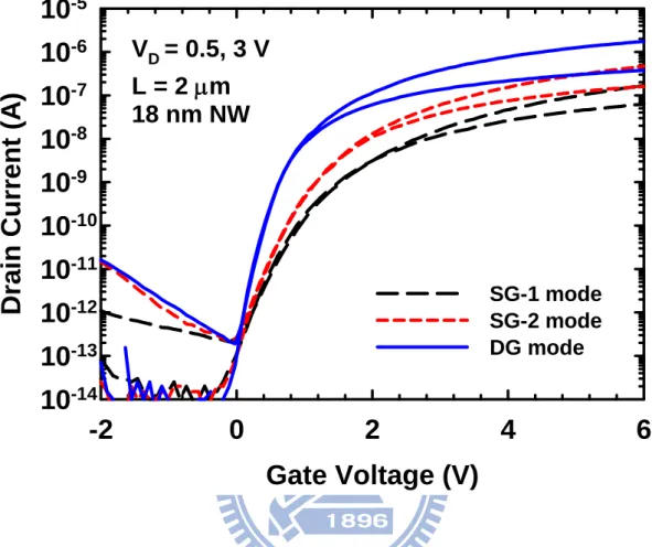
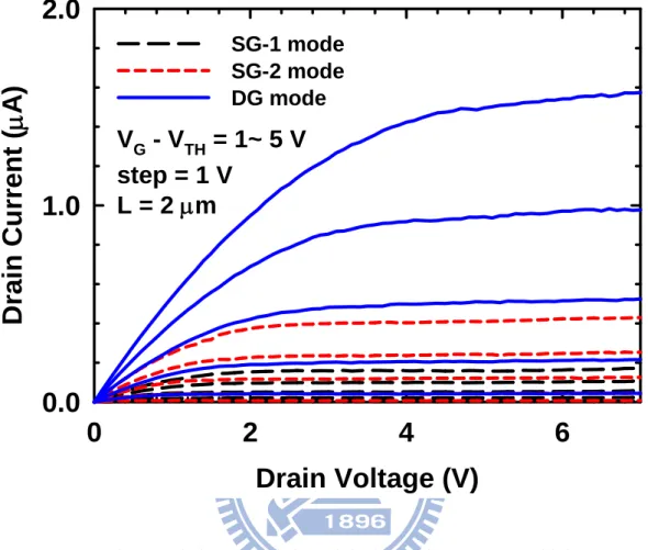
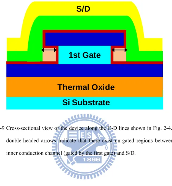
double-gated poly-Si NW TFT showing 18-nm NW thickness. ... 66 Fig. 2-7 Transfer characteristics of a fabricated device with 18-nm NW thickness. ... 67 Fig. 2-8 Output characteristics of a fabricated device with 18-nm NW thickness. ... 68 Fig. 2-9 Cross-sectional view of the device along the C-D lines shown in Fig. 2-4. The double-headed arrows indicate that there exist un-gated regions between the
inner conduction channel (gated by the first gate) and S/D. ... 69 Fig. 2-10 Transfer characteristics for devices with various numbers of NW channels. It is seen that the VTH and SS are independent of the number of NW channels,
suggesting good uniformity among the measured devices. ... 70 Fig. 2-11 GM characteristics for a device with 18-nm NW extracted from Fig. 2-7.
Higher GM can be obtained in DG mode over the other two SG modes. ... 71
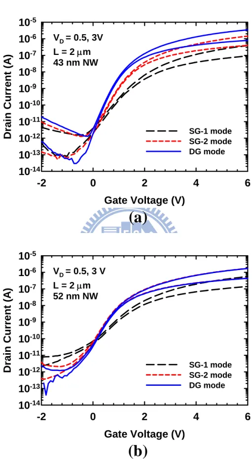
Fig. 2-12 Drain current ratio vs. drain voltage with gate overdrive as a parameter for a device with 18-nm NW extracted from Fig. 2-8. For all the measured drain voltage range, the output current under DG mode is larger than the other two SG modes combined. The drain voltage at which the ratio saturates increases with increasing gate overdrive, which is ascribed to the “early saturation effect” in SG modes [2-23]. ... 72 Fig. 2-13 Transfer curves for devices with (a) 43- and (b) 52-nm-thick NW channels. 73 Fig. 2-14 Comparison of GM ratio characteristics among devices with three different
NW thicknesses. The peak of ratio is 2.4, 1.8, and 1.2 for a device with 18-, 43-, and 52-nm-thick NW channels, respectively. ... 74 Fig. 2-15 Extracted total resistance as a function of the gate voltage under DG and
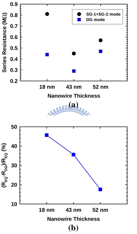
SG-1+SG-2 modes. ... 75 Fig. 2-16 (a) Series resistance under SG and DG modes extracted by the procedure in
Fig. 2-15. (b) Percentagewise series resistance reduction under DG mode in comparison with SG modes as a function of NW thickness. ... 76 Fig. 2-17 SS under three operation modes as a function of NW thickness. For all three
modes, SS is observed to decrease with reduced NW thickness. ... 77 Fig. 2-18 Extracted barrier height under SG and DG modes as a function of the gate
overdrive for devices with (a) 18-nm, (b) 43-nm, and (c) 52-nm NW channels. ... 78 Fig. 2-19 Comparisons of size-dependent barrier height reduction capabilities under
DG mode. The lowering rate is larger as the size of NW is thinner. ... 79 Fig. 2-20 Transfer characteristics of an 18-nm NW device with varying AG bias under (a) SG-1 and (b) SG-2 modes. AG bias ranges from -3 V to 3 V in step of 0.5 V. VTH is seen to be effectively adjusted by different AG bias. ... 80
Fig. 2-21 Dependency of VTH as a function of applied AG voltage when the 1st gate or
2nd gate assumes AG extracted from Fig. 20. The higher VTH sensitivity to the
2nd gate voltage is a result of its stronger controllability over NW channels. 81 Fig. 2-22 Transfer characteristics of NW devices with NW thickness of (a) 43-nm and
(b) 52-nm NW device with varying AG bias under SG-2 mode. In comparison with Fig. 2-20, the extent of VTH distribution with respect to AG bias is much
Chapter 3
Fig. 3-1 Schematic process flow for the double-gated poly-Si NW TFT with in situ doped S/D. (a) Sequential deposition of 100-nm thermal oxide, 50-nm nitride, 100-nm in situ doped N+ poly-Si, and 50-nm nitride on a 6-in Si wafer. First gate patterning was then performed. (b) Selective plasma etching of the first gate. (c) First gate dielectric (20-nm TEOS oxide) and 100-nm amorphous-Si layer deposition followed by SPC. (d) Dry etching to form NWs underneath the hard mask and a spacer-like portion of poly-Si along the sidewall of the first gate. (e) Deposition of 100-nm in situ phosphorus doped poly-Si. (f) Simultaneous definition of NW channels and S/D regions using dry etching. (g) Second gate stack (20-nm LPCVD TEOS oxide and 100-nm in situ doped N+ poly-Si) deposition and patterning. ... 101 Fig. 3-2 Cross-sectional TEM image of an independent double-gated NW transistor
with in situ doped S/D. ... 102 Fig. 3-3 Transfer characteristics of a fabricated device with implanted S/D. ... 103 Fig. 3-4 Transfer characteristics of a fabricated device with in situ doped S/D. SS
under DG mode is 73 mV/dec, the best value ever reported for a poly-Si based device. ... 104 Fig. 3-5 Fluctuation analysis of devices with (a) implanted S/D and (b) in situ doped
S/D. Twenty devices are measured in each figure. ... 105 Fig. 3-6 SS as a function of channel length for the in situ doped device. ... 106 Fig. 3-7 Output characteristics comparison between devices with implanted and in situ doped S/D under (a) DG, (b) SG-1, and (c) SG-2 modes. ... 108 Fig. 3-8 Extraction of S/D series resistance showing five times reduction with the
adoption of in situ doped S/D. ... 109 Fig. 3-9 ION-IOFF statistical analysis comparison between devices with implanted and
in situ doped S/D. ... 110
Fig. 3-10 (a) Schematic of the device structure before the 2nd gate stack deposition. GIDL current conduction paths in the circled area of (a) are depicted for (b) implanted S/D and (c) in situ doped S/D type devices. ... 111 Fig. 3-11 Extracted activation energy of IOFF as a function of gate underdrive for
devices with implanted and in situ doped S/D. Implanted S/D type device displays a stronger dependency on the gate voltage, suggesting the dominant role of GIDL in determining IOFF. ... 112
Fig. 3-12 Schematic band diagrams at the off state under two different gate biases. (a) For a sufficiently negative gate bias, BTBT dominates. (b) Under medium electric field regime, electrons are thermally activated to the trap state (ET)
tunneling or thermionic field emission. ... 113 Fig. 3-13 (a) Plane-view SEM image of a 100-nm thick poly-Si layer obtained by SPC whose average grain size is around 60 nm. (b) Plane-view TEM image of a 100-nm thick in situ doped poly-Si layer whose average grain size is around 200 nm... 114
Chapter 4
Fig. 4-1 Layout of the device fabricated using mix-and-match between e-beam and I-line. L defines the channel length, which is smaller than 100 nm in this case. ... 135 Fig. 4-2 (a) Plane- and (b) cross-sectional view images of a fabricated device showing a 23-nm-thick NW channel surrounded by the 1st and 2nd gates. The drastic grain size discrepancy between the 1st and 2nd gates is a consequence of the different doping method implemented: the 1st gate is by in situ doping while the 2nd gate by implantation. ... 136 Fig. 4-3 Length-dependent transfer curves at 25oC under (a) SG-1, (b) SG-2, and (c)
DG modes. ... 137 Fig. 4-4 SS as a function of L extracted from Fig. 4-3. ... 138 Fig. 4-5 Transfer characteristics at various temperatures for a device with 70 nm
channel length under (a) SG-1, (b) SG-2, and (c) DG modes. The behavior of SG-1 mode is in accordance with thermionic emission model while SG-2 mode starts to exhibit very steep SS when T is below150 K. Abrupt increase of ID for DG mode at 100 K and 78 K is caused by the channel controlled by
the 2nd gate. ... 140 Fig. 4-6 (a) SS and (b) VTH as a function of temperature for three operation modes
extracted from Fig. 4-5. Ideal value of SS equal to ln10 × kT/q is also included for comparison in (a). ... 141 Fig. 4-7 Transfer characteristics at 78 K showing impacts of L in determining the
occurrence of steep SS. In conflict with the conventional SCE theory, the subthreshold current is reduced as L is shortened. ... 142 Fig. 4-8 Schematic structures along the length direction showing the 2nd
gate-controlled side of channel for a device whose L is (a) long (> 100 nm) and (b) short (< 100 nm). Points A and C correspond to regions of the channel adjacent to S/D controlled by the locally thickened gate and point B to the middle of the channel. Because the thickness of the 2nd gate is 100 nm, the part of the 2nd gate between S/D is thicker in (b) than in (a). ... 143 Fig. 4-9 Simulated dopant distribution in an implanted gate corresponding to a device
the 2nd gate has much lower concentration in (b) than in (a). ... 144 Fig. 4-10 (a) TEM image of a non-overlapped NMOSFET with 16 nm gate length. The
notched gate is fabricated by selective etching of poly-SiGe. (b) Simulated electrostatic channel potential profile under two different gate voltages. As the gate voltage is increased, the potential valley drops to a larger extent than the humps in the non-overlapped regions, facilitating the formation of a quantum dot. Adapted from [4-18]. ... 145 Fig. 4-11 Qualitative band diagrams for devices with long and short L. Points A, B, and C correspond to the regions labeled in Fig. 4-8. For a short channel device, thermionic emission is the dominant transport mechanism while both thermionic emission and tunneling should be considered for a long channel device. ………...146 Fig. 4-12 Proposed model for the origin of steep SS. (a) For a low 2nd gate voltage (VG2
= V1), after electron trapping in the channel (dashed line), the potential is
raised from its original level (solid line), which deters further injection from the source. (b) For a larger 2nd gate voltage (VG2 = V2) that considerably
reduces the barrier height at drain side, electrons are detrapped and flow to the drain, leading to channel potential drop (dotted line) and an abrupt increase of drain current. ... 147 Fig. 4-13 Transfer characteristics as a function of temperature for a device whose 1st
and 2nd gates are both in situ doped. Compared with Fig. 4-5 (b), steep SS completely vanishes owing to the removal of barriers when very uniform doping concentration throughout the whole 2nd gate electrode is achieved by
in situ doping. ... 148
Fig. 4-14 Drain-voltage-dependent transfer characteristics suggest DIBL could eliminate the occurrence of steep SS, in agreement with the proposed model……. ... 149 Fig. 4-15 Transfer characteristics under SG-2 mode for various VG1 at (a) 150 K and (b)
78 K. VG1 here ranges from -1 V to 1 V in 0.5 V step. ... 150
Fig. 4-16 Transfer characteristics for a device with L = 5 μm under forward and reverse sweeping of the gate voltage for (a) SG-1, (b) SG-2, and (c) DG modes…….…. ... 151 Fig. 4-17 Transfer characteristics for a device with L = 63 nm under forward and
reverse sweeping of the gate voltage for (a) SG-1, (b) SG-2, and (c) DG modes……. ... 152 Fig. 4-18 Forward and reverse sweeping of transfer characteristics with (a) the drain
voltage and (b) temperature as a parameter. ... 153 Fig. 4-19 Oscillation of the drain current and resultant GM at 1 mV VD. ... 154
Fig. 4-20 Output characteristics showing a wider current blockade region at a lower gate voltage. Different kink points in the positive and negative drain voltage regime indicate the presence of asymmetric barriers. ... 155 Fig. 4-21 Transfer characteristics measured by interchanging the applied biases to S/D
showing two distinct curves, an indication of the asymmetry between source and drain barriers, in agreement with Fig. 4-20. ... 156
Chapter 5
Fig. 5-1 Wiring of (a) NAND and (b) NOR flash memory. (c) Major operation features of NAND and NOR flash memory [5-17]. ... 184 Fig. 5-2 Schematic diagram illustrating CHEI. The filled and hollow dots represent
electrons and holes, respectively. Electrons in the inversion channel would be accelerated by the applied high drain bias and absorb significant amount of kinetic energy especially in the pinch-off region near the drain side where strong lateral electric field exists. Those “hot” electrons along with secondary electrons created by the impact ionization would then be injected into the gate dielectric provided they are “lucky” enough. ... 185 Fig. 5-3 An energy band diagram illustrating F-N tunneling. When a positive gate
voltage bias is applied such that the voltage drop across the oxide is larger than the conduction band offset between Si substrate and the oxide, mobile electrons in the conduction band of Si see a triangular-shaped energy barrier and may tunnel through the oxide into the gate. ... 186 Fig. 5-4 (a) TEM image of a fabricated double-gated poly-Si NW SONOS TFT. (b)
Graphic representation for indicating the composition of the gate dielectrics and notation for the applied biases. ... 187 Fig. 5-5 (a) Programming speed characterization with VG1 as a parameter while VG2 is
fixed at 16 V. (b) Transfer curves corresponding to (a) showing that a larger VG1 applied during programming stressing could result in an enhanced VTH
shift. ... 188 Fig. 5-6 (a) Erasing speed characterization with VG1 as a parameter while VG2 is fixed
at -13 V. (b) Transfer curves corresponding to (a) showing that a larger VG1
applied during erasing stressing could result in an enhanced VTH shift. ... 189
Fig. 5-7 Transfer curves under P/E states with varying AG bias when the device is read by (a) SG-1 and (b) SG-2 modes. Programming and erasing are achieved by applying VG1 = 0 V and VG2 = 16 V for 10 ms, and VG1 = 0 V and VG2 =
-12 V for 100 ms, respectively. ... 190 Fig. 5-8 Extracted VTH under programmed and erased states (left vertical axis) from
SG-1 and (b) SG-2 modes. Depending on the condition of the back surface, the magnitude of γ for each operation regime is indicated. ... 191 Fig. 5-9 Programming speed comparison between two read modes. The SG-1 mode
shows higher efficiency than the SG-2 mode for up to 20 msec. Programming conditions are VG1 = 0 V and VG2 = 14 V, and VG1 = 0 V and VG2 = 18 V for
curves with circles and squares, respectively. ... 192 Fig. 5-10 Erasing speed characterization showing that SG-1 mode does not exhibit any VTH shift until 10 msec after which a substantially decreased VTH value is
observed for SG-1 mode with VG2 = 3 V. Erasing speed as read by SG-1 mode
is enhanced with a larger VG2 since inversion would be reached earlier by a
larger VG2 in a given erasing time. ... 193
Fig. 5-11 Schematic of the evolution of VTH- VG2 curves during (a) programming and
(b) erasing when read by SG-1 mode. Owing to the selected VG2 (= 3 V) and
the back-gate effect, an appreciable VTH shift during programming can
initially be obtained compared with negligible VTH shift during erasing. ... 194
Fig. 5-12 Endurance characteristics of (a) SG-1 and (b) SG-2 modes. The more serious variation of VTH at the erased state of SG-1 than SG-2 mode is caused by the
back-gate effect. ... 195 Fig. 5-13 Evolution of transfer curves in P/E states with the number of cycling as a
parameter when the device is read by (a) SG-1 mode with VG2 = 3 V and (b)
SG-2 mode with VG1 = 0 V. ... 196
Fig. 5-14 Schematic diagram showing the 2nd gate stack. TOX1, TN, and TOX2 are the
respective thicknesses of the blocking oxide, nitride, and tunneling oxide. If the trapped electron density located in the middle of the nitride is Qtot, then
the flat-band voltage shift as compared with the fresh state (i.e., Qtot = 0) is
equal to ) 2 ( 0 0 1 N N OX OX tot T T Q ε ε ε ε + . ... 197 Fig. 5-15 Schematic illustration of how VTH in SG-1 mode responds to the change in
the storage charge. Blue and red lines represent the condition when the density of the storage charge in the nitride layer is varied such that the transition point is shifted horizontally by ∂(ΔVFB)|SG−2. The resultant VTH
shift under SG-1 mode would then be equal to γ∂(ΔVFB)|SG−2 ... 198 Fig. 5-16 Baked retention characteristics indicating that VTH of the programmed state in
SG-1 mode is lowered to a lesser extent than that of SG-2 mode while these two modes are comparable in terms of their VTH enlargement at erased
states……… ... 199 Fig. 5-17 (a) Schematic illustration of the device configuration for 2-bit/cell
characterization. Bit-1 and bit-2 refer to the bit located in the nitride of the 1st and 2nd gate dielectrics, respectively. (b) Four distinguishable states can be observed when the dielectrics of both gates are made up of ONO, thus realizing the 2-bit/cell feature. VTH difference between state-11 and -00 is 5.3
V…………. ... 200 Fig. 5-18 (a)(b) Programming and (c)(d) erasing disturbance characterization for
2-bit/cell operation. Decent P/E speed is attained without significant disturbance. The measured device is with 50-nm-thick NW channels. ... 201
Appendix
Fig. A-1 XRD profiles of samples undergoing SPC at different temperatures for 2 hr. Major orientations of poly-Ge are identified as (111), (220), and (311). The result for a fresh sample is also included for comparison. ... 228 Fig. A-2 XRD results of samples undergoing SPC at 500 oC for different durations
ranging from 0.5 hr to 6 hr. Peak intensities are observed to increase only within the initial 1 hr of annealing and then remain constant. ... 229 Fig. A-3 Cross-sectional TEM image of the poly-Ge film annealed at 500 oC for 1
hr………… ... 230 Fig. A-4 AFM surface analysis of the poly-Ge film annealed at 500 oC for 1 hr for a
sample (a) without and (b) with the oxide capping layer during annealing. 230 Fig. A-5 Schematic structure for the proposed poly-Ge TFT. ... 231 Fig. A-6 Transfer characteristics of the proposed poly-Ge TFT. ... 231 Fig. A-7 AFM images in phase mode of two sputtered Ge on Si samples deposited
with (a) 2 W RF bias (DC bias = 43 V) to the substrate and (b) 5 W RF bias (DC bias = 61 V) to the substrate, respectively. ... 232 Fig. A-8 XRD profiles of one sputtered Ge on Si sample after 600 oC 2 min RTA
annealing. It was sputtered by 300 W of source power for 700 sec with 2 W RF (DC bias = 43V) bias applied to the substrate. The final Ge thickness is 200 nm….. ... 233 Fig. A-9 EBSD patterns of the Ge film at three different spots (a, b, c). Results: Ge
film is polycrystalline with very small, tens of nm, grain size. Insets in (a, b, c) with simulated orientation of Ge unit cell indicate random crystallographic orientations of Ge grains. ... 234
Chapter 1
Introduction
To maintain the momentum of CMOS scaling, multiple-gated nanowire (NW) devices have been proposed as one of the most promising future transistor structures [1-1], due to the better gate controllability to suppress the short channel effects (SCEs). NW, basically, can be defined as a narrow stripe material with its cross-sectional feature size less than 100 nm. It has been conceived as an ideal building block for nanoelectronics and optoelectronics. One unique feature of NW lies in its very tiny volume and large surface-to-volume ratio, thus making it suitable for a wide array of applications. For memory applications, fast programming/erasing efficiency and low voltage operation can be facilitated and the large surface-to-volume ratio feature promotes high sensitivity for sensor applications. As a result of the tiny cross section of NW body, confinement of carriers in the plane perpendicular to the channel direction can occur. Already a plethora of intriguing phenomena are associated with this nano-scale structure, such as Coulomb blockade [1-2], quantized conductance [1-3], and reduced phonon scattering [1-4], to name just a few.
Though most of the previous works regarding NW research focused on single-crystalline Si based technology for realizing high performance CMOS transistors,
recently a new concept of NW based thin film transistors (TFTs) has started to gain attention [1-5][1-6]. Compared to single-crystalline Si wafer technology, TFT devices completely eliminate the need for a high-cost substrate. This merit is especially profound when prohibitive silicon-on-insulator (SOI) architecture starts to emerge as another substrate alternative in order to promote the fabrication of multiple-gated device such as FinFETs [1-7]. For the macroelectronics industry where it is preferred to construct electronic devices and components over a large area substrate, TFT architecture is a promising option since it merely requires a thin active layer to be deposited onto an insulating substrate. Therefore, glass and plastic substrates become the primary choice as they are flexible, light weight, and most importantly, cheap. Below an overview of NW technology is briefly given.
1.1 Overview of Nanowire Technology
Gordon Moore in 1965 predicted that the number of transistors in a chip would double every two years [1-8]. Even though it takes eighteen months to be exact for the number to increase by twofold, this prediction has been termed “Moore’s law” and has become the guiding principle of the semiconductor industry for the past few decades. To follow this path mainly depends on the downsizing of transistors. The potential of constant electric field scaling was recognized in a renowned paper by Robert H.
Dennard et al [1-9] that underlies Moore’s law. Yet as the last half-century has seen a relentless miniaturization of electronics in pursuit of high performance CMOS technology, the physical limit of geometric scaling is imminent as the transistor dimension approaches only a few tens of nanometers [1-10]. Among the various structures ever proposed, NW is recognized as the most promising one to suppress SCEs and sustain the scaling path for nano-scale MOSFETs [1-11]. With NW, many possible and interesting applications have also been explored [1-12]. There are generally two types of methods for the preparation of NW, termed top-down and bottom-up, to be described as follows.
1.1.1 Top-down Approach
This approach typically employs advanced lithographic tools (e-beam [1-13] or deep ultraviolet (DUV) [1-14]) to directly generate nano-scale photoresist patterns, which are then transferred to the underlying SOI substrate by dry etching. This kind of process can precisely control and align the structural parameters and minimize variations of devices, so it is suitable for mass production though at the sacrifice of high manufacturing cost. Current state-of-the-art technology is able to generate line width less than 40 nm and with the aid of some innovative skills including trimming, double-patterning, hydrogen annealing, self-limiting oxidation, and thermal flow, etc., critical dimension down to sub-10 nm can be achieved [1-14]-[1-16]. Major
shortcomings of this procedure are the associated expensive exposure apparatus and substrate materials as well as the inflexible choice of NW material due to the limited selection of substrates.
1.1.2 Bottom-Up Approach
A detailed and comprehensive review of this approach can be found in [1-12] and [1-17][1-18]. This approach is mainly based on chemical processes to synthesize and grow NWs of various kinds of materials. After NWs are synthesized, they are harvested and dispersed into a solution, which are then deposited onto an oxidized substrate (to serve as the back gate) followed by metal electrodes attachment to complete a field effect transistor structure. Vapor-liquid-solid (VLS) [1-19] is the most well-established mechanism to produce NW. In this procedure, the metal nanocluster is first heated in the ambient of gas-phase reactants of the semiconductor material to be synthesized. When the nanocluster is heated to above the eutectic temperature, liquid droplet of the metal/semiconductor is formed. Continuous supply of semiconductor reactants then supersatures the cluster, resulting in nucleation and directional growth of a wire-like structure. The dominant growing direction (axial or radial) is found to be intimately related to the growth process conditions, such as the temperature, flow rate, reactant species, and pressure. Single-crystalline NW can be obtained using this method. In the
catalyst and reactant, respectively. Since the material of NW to be produced depends on the precursors used, III-V and II-VI NWs have also been prepared besides Si [1-20]. In this regard, in comparison with top-down, bottom-up is far more flexible in terms of the NW material that can be obtained. Nevertheless, metal contamination is a major concern for metal-catalyzed growth. Oxide-assisted growth [1-21] without the need for metal-catalyst could get rid of this issue, but the NW thus formed could contain plenty of defects.
In short, bottom-up approach is definitely the better choice for experimental purposes because it is cheap and can grow various kinds of materials. However, it is plagued by several shortcomings as well. First, reproducible transfer and precise control of structural parameters of NWs are very difficult to accomplish. Alignment and positioning are daunting tasks that are hard to overcome. To fabricate reliable contacts between metal and NWs requires sophisticated manipulation and poses as another showstopper for bottom-up approach.
To this end, in this dissertation we propose and develop a novel technique for the fabrication of Si NW devices that without any compromise combines all the merits of top-down and bottom-up approaches, namely, cost effectiveness, good reliability and reproducibility, and CMOS-compatibility.
1.2 Multiple-Gated
Devices
Faced with an ever greater challenge of fabricating a “well-behaved” transistor for which SCEs are minimized in the era of 32 nm technology node and beyond, a number of new processing schemes have been embraced to address this issue. For the purpose of resolving poly-gate depletion and alleviating non-negligible gate dielectric tunneling current, high-κ/metal gate is being pursued actively and is already adopted in commercial 45 nm microprocessors of Intel [1-22]. Another option of relieving SCEs is to resort to multiple-gated configuration. As the name suggests, in a multiple-gated transistor, the active layer is controlled by more than one gate as opposed to planar single-gated counterparts. This kind of structure is capable of effectively preventing the drain field penetration that weakens the gate controllability over channels thereby leading to SCEs. On account of the better electrostatic control of channels, for a given channel width, larger driving current can be provided by multiple-gated configuration. Of all the multiple-gated structures ever proposed so far, FinFET is considered as the one most appropriate for practical applications because it is actually quasi-planar and is most compatible with modern ULSI (ultra large scale integration) technology [1-23]. Moreover, the conduction width in FinFET, which is determined by the fin height, is along a direction that is normal to the substrate plane. This vertical feature offers an improvement in density that is not restricted by the resolution of lithographic tools.
Evolving from the original double-gated structure, several variations of FinFET have been reported, including tri-gate [1-24] and Ω-gate [1-25]. In particular, the gate-all-around type device where the channel is fully wrapped by a surrounding gate is considered the most ideal structure to proffer the best gate controllability over the channel [1-26]. Selected devices of NW or FinFET structure with sub-20 nm channel length are listed in Table 1-I.
1.3 Transport Behavior of Nanowire Devices
The paradigm shift caused by NW creates whole new concepts and perspectives on device physics and possibilities that conventional planar counterparts have yet to offer. From a microscopic point of view, this kind of low-dimensional structure is suitable for studying quantum-mechanical effects. Many reports focused on the carrier transport properties in NW devices for which well-established theories of three- or two-dimensional materials are no longer appropriate. Energy bands are split into sub-bands and the energy levels become discrete by the tiny volume of NW [1-30]. Because of the nano-scale cross section that confines the wave functions of sub-bands, carriers in NW devices must transport through a large number of one-dimensional sub-bands. Quantum confinement, sub-band splitting, and surface and interface relaxation [1-31]-[1-33], etc. are among a plethora of effects that must be taken into
account in order to correctly interpret the NW characteristics, including unexpected increase of threshold voltage (VTH) with reduced NW width [1-34], oscillation of drain
current and mobility [1-32], and reduced Stark effect [1-35]. Recently, dopant distribution has been identified as another major factor in influencing the carrier conduction behavior in ultra-short NW devices [1-36]. Simulation results have shown that NW transistors may approach ballistic transport [1-37], i.e., a carrier does not experience any collision with other carriers or elastic centers during its traverse from the source toward the drain. In the quasi-ballistic model proposed by Lundstrom [1-38][1-39] where there is no sufficient scattering events occurring inside a short channel MOSFET device, backscattering effects near the source start to become prominent, but since this effect is linked to the source side mobility, the concept of mobility is still relevant. On the other hand, if the channel length is scaled further (less than 10 nm [1-40]), no scattering events would occur and in this scenario the transport of carriers operates in the full ballistic regime. Drain current under ballistic transport has been shown to depend only on the carrier concentration near the source and the injection velocity at the peak of the barrier at the source side [1-41][1-42], which is determined solely by the thermal velocity in the case of non-degeneracy. Thus, the concept of mobility becomes meaningless, leading to a profound change of mindset on how the carrier transport properties should be examined. For typical short channel planar devices,
scattering defects associated with pocket implant near source/drain junctions result in mobility degradation as the channel length is made shorter [1-43][1-44]. Even though NW exhibits similar behavior that the “extracted” mobility tends to decrease with reduced channel length, this is essentially an artifact and can be explained by the “ballistic mobility” model [1-45]. As a matter of fact, since NW has entered into ballistic regime, the measured mobility no longer determines the transport property and the actual transport behavior will not degrade with channel length scaling [1-46]. In other words, not only does NW device possess better immunity against SCE, it is also promising to provide ballistic transport when being downsized to ultra-short channel lengths. Another intriguing effect exclusive to NWs is that the drain current of linear regime (low VD) in strong inversion is found to decrease with decreasing temperature,
which is shown to be caused by the inter-sub-band scattering induced by quantum confinement [1-32]. Yet, in saturation regime (high VD), this effect is diminished and the
mobility-temperature relationship again resorts to what is dictated by phonon scattering. In addition, differential conductance fluctuations are observed in output curves as the series resistance of the drain extension is changed by the interplay between inter-sub-band transitions and quasi-ballistic transport [1-47].
One concept called “quantum capacitance limit” introduced recently further highlights the performance advantage of 1-D NW device over bulk counterparts in
terms of the power delay product improvement that can be achieved from scaling [1-48]. To realize a well-behaved device that exhibits electrostatic integrity, two major conditions should be fulfilled. First, the maximum of surface potential in the channel that governs the injection of carriers from the source is mainly modulated by the gate voltage instead of the drain voltage. Second, the oxide capacitance ought to be much larger than the inversion layer or quantum capacitance, which is the change of channel charge with respect to the surface potential. The first condition is always met as long as the channel length is much longer than the natural scaling length [1-49], whereas the second one is dependent on the operation state of the device. In the off-state, the quantum capacitance is nearly zero because the channel charge shows little variation. However, in the on-state, this capacitance is proportional to the density of states present in the channel [1-50], which increases with the gate voltage in a bulk device. Accordingly, the modulation of the surface potential is less efficient in the on-state, explaining the gradual increase of the subthreshold swing with a larger gate voltage of a conventional device. The scenario is vastly different in the case of 1-D NW device for which the density of states is inversely proportional to the square root of the difference between the carrier energy and surface potential [1-50]. Consequently, it is easier for NW to reach the so-called quantum capacitance limit, where the gate dielectric capacitance readily exceeds the quantum capacitance and the gate electrode is still able
to provide ideal control of the surface potential in the on-state. In other words, the thickness of the gate dielectric in a 1-D NW transistor required to meet the criterion of quantum capacitance limit can be thicker and is much more technologically feasible than the bulk devices.
To fully capture the underlying physical mechanisms of NW requires devices with sub-10 nm channel length, which are still difficult to fabricate if not impossible [1-15], thus most works only use theoretical formalism to predict the transport behavior of NW devices. Some commonly utilized ones are Boltzmann transport equation [1-51], non-equilibrium Green’s function (NEGF) [1-52][1-53], and quantum diffusion method [1-54]. Each of these approaches is suitable only for some specific conditions depending on the temperature and channel length considered. Additional approximations are needed as well to simplify the complexity of NW band structures and reduce the computational time. Hence, it still takes further advance in process technology and development of more precise theoretical modeling to gain a comprehensive insight into the potential of NW transistors.
1.4 Overview of Nonvolatile Memory Technology
As portable electronic products have already become indispensable components of daily life, nonvolatile memory technology is being used in a wide array of commodities,
including cell phones, USB drives, memory cards, etc. Being one of the two types of semiconductor memory, nonvolatile memory retains its stored data even if the power is turned off as opposed to volatile memory where the data are immediately lost as soon as the power is turned off. This unique property makes nonvolatile memory an ideal choice for low power portable electronic products.
The first nonvolatile memory device was reported in 1967 by D. Kahng and S. M. Sze at Bell labs [1-55]. The gate stack is a five-layered structure consisting of metal-oxide-metal-oxide-semiconductor. As charges are stored in the metal that is surrounded by two dielectrics, this is called floating-gate (FG) type nonvolatile memory. Even though along the way there are plenty of variations in terms of the charge storage layer and the stack composition or thickness (e.g., MNOS [1-56], FAMOS [1-57], EToxTM [1-58] and SAMOS [1-59]), FG is still the mainstream technology to date in which the storage layer is now made of poly-Si. Of all the different types of memory technology nowadays, Flash memory with FG structure has gained a lot of attention owing to its particular features, such as low cost, low power consumption, good endurance, high density, and long data retention capability. In Flash memory, program/erase stressing can be performed repetitively up to 105 cycles without significant degradation or loss of stored data. Another advantage involves the byte-selectable program operation and block “flash” erasure. Unfortunately, as the
feature size is made smaller with each technology node, several scaling challenges have emerged. Hence, charge-trapping-type Flash, to be discussed below, was proposed to succeed FG as the next generation Flash memory technology by Samsung in 2005 [1-60].
1.4.1 Charge Trapping SONOS Memory
Aggressive scaling of conventional FG type memory device has encountered quite a few issues that must be seriously dealt with, including narrow FG-FG space to contain control gate, FG-FG interference coupling, read or program noise, stress-induced leakage current (SILC), and severe SCEs [1-61]. To address those issues, charge-trapping type nonvolatile memory devices, with nitride read-only memory (NROM) [1-62] and Si-oxide-nitride-oxide-Si (SONOS) [1-63] being the mainstream, have recently emerged as new promising candidates for continuing the miniaturization trend, together with other innovative nonvolatile memory concepts, including ferroelectric and magnetoresistive memories [1-64], phase-change memory [1-65] and unified random access memory [1-66] that has claimed to have both volatile and nonvolatile functionalities. Among these devices, SONOS, with a plethora of variations such as bandgap engineered (BE) SONOS [1-67], Ta-AlO-Nitride-Oxide-Si (TANOS) [1-68], etc, has shown its high performance and promising potential for future Flash
memory applications.
In its basic structure, SONOS uses a non-conductive nitride layer for storing charges compared with conductive poly-Si in FG. As a consequence, charges are discretely stored in the nitride and a single defect present in the tunneling oxide would not cause all stored charges to leak out. Combined with the deep energy level of nitride for charge storage, retention characteristics can be dramatically improved. As in NROM, by storing charges at two different sites in the nitride (e.g., source-side and drain-side), 2-bit/cell operation is feasible. In addition, because the stack height of SONOS is much more reduced over that of FG, interference coupling is suppressed to a great degree, which is helpful for further advancement of device scaling. Recently, TFT-based SONOS devices have been investigated in an effort to realize system-on-panel (SOP) or system-on-chip (SOC) applications [1-69]. TFTs could also facilitate 3D integration technology [1-70] which greatly improves interconnect density, reduces cost and provides a platform for heterogeneous integration.
1.4.2 Nanowire-Based Nonvolatile Memory
Besides being able to scale device dimensions down to nano-scale regime without sever SCEs, NW can be useful for nonvolatile memory technology as well. Owing to its large surface-to-volume ratio property, NW is highly sensitive to its surface conditions.
Making use of this feature, the threshold voltage of a memory device can be altered to a large extent by a small amount of stored charges, allowing reduced program/erase operation voltage and stressing time to obtain a sufficient memory window.
Most of the reports concerning NW nonvolatile memory devices rely on the formation of a charge storage layer upon the NW surface to adjust the threshold voltage of the device. For the purpose of achieving larger voltage drop across the tunneling layer, SONOS device integrated with gate-all-around configuration has been demonstrated [1-71]. And to prevent some undesirable effects such as electron back-tunneling from the gate electrode and insufficient electric field across the tunneling oxide, an optimized version called TAHOS (TaN/Al2O3/HFO2/SiO2/Si) was
reported to significantly improve both programming and erasing speeds [1-72].
1.5 Motivation
NW transistors have revealed their promising potential in a wide variety of applications. Development of high performance NW devices with reliable and reproducible processes is urgently needed. To cope with the issues encountered in top-down and bottom-up approaches introduced in Section 1.1, our lab (Advanced Device Technology Laboratory) has proposed several innovative procedures of fabricating poly-Si NW TFTs using low cost and simple methods [1-73]-[1-76]. The
first type in [1-73] employed sidewall spacer etching technique to define simultaneously poly-Si NW channels and source/drain regions followed by another modified version where inverse-T and top gates were formed to fulfill a multiple-gated configuration [1-74]. Though our proposed scheme belongs to the top-down category, it includes the merits of both top-down and bottom-up approaches without their drawbacks. In [1-73]-[1-75], after deposition and anisotropic etching, poly-Si NWs are formed along the sidewall of a pre-formed gate. Major benefits of this method are listed as follows.
1. Precise alignment and positioning of NWs.
2. Well-controlled NW size as it is related to the thickness of the deposited film and the etching duration.
3. Self-alignment between NW channels and source/drain regions. 4. CMOS compatibility.
In spite of all these advantages, its triangular shape may have hindered its practical applications and it may suffer severe SCE if the channel length is to be further scaled down since the electric field is very likely to be concentrated on a certain vertex. In the mean time the irregular shape makes it difficult for an accurate theoretical modeling. To solve this dilemma, we come up with a modified independent double-gated TFT with rectangular NW channels. Such a design allows more flexibility in device operation and may help improve reliability characteristics in nonvolatile memory applications.
1.6 Organization of the Dissertation
Six chapters are contained in this dissertation. Background and motivation are described in Chapter 1. Chapter 2 discusses the device structure, fabrication process, and basic electrical characteristics of the main device architecture proposed in this study. Source/drain engineering for performance enhancement is investigated and analyzed in Chapter 3. Study on the transport behavior at cryogenic ambient is conducted in Chapter 4. Chapter 5 details the merits offered by independent double-gated configuration in SONOS memory devices. In Chapter 6, major achievements and summary are stated, and suggested future works are listed. The following specifies the detailed content of each chapter.
In Chapter 1, overview of NW technology and multiple-gated devices are mentioned along with a brief description of NW transport properties and nonvolatile memory technology. As noted in the motivation, to deal with some dilemma of NW fabrication process and to optimize the structure of our previously reported device, a novel independent double-gated poly-Si NW transistor with rectangular channels is thus proposed.
Chapter 2 elucidates the structure and fabrication process of the proposed poly-Si NW devices. An isotropic and selective plasma etching technique is explored to form a
rectangular-shaped NW. Subsequently, impacts of different operation modes associated with the double-gated configuration on device performance are discussed followed by the examination of the root cause for the size dependency, which is found to be intimately linked to the capability of the gates in adjusting the magnitude of grain boundary barrier height.
In Chapter 3, source/drain engineering is investigated to enhance device performance. Replacing ion implantation with in-situ doping for the formation of source/drain regions, it is demonstrated that the overall electrical characteristics are clearly improved and a record-breaking 73 mV/dec subthreshold swing is achieved.
In Chapter 4, to probe the underlying transport properties, devices with channel lengths ranging from 39 nm to 5 μm are fabricated and characterized under cryogenic ambient. A very intriguing abrupt switching phenomenon is observed when the device is operated under one of the two single-gated modes. In addition, this behavior shows a strong dependency on the channel length that is in obvious conflict with the conventional theory concerning SCE as the subthreshold current is reduced with shorter channel length. A simple model based on the barrier formation near the source/drain due to non-uniform gate doping is proposed to explain this phenomenon.
In Chapter 5, the influence of independent double-gated configuration on SONOS type nonvolatile memory applications is discussed. In contrast to the convention where
the programming/erasing gate also acts as the read gate, a dedicated read gate with oxide-only dielectric is proposed in the new mode. Greatly improved programming speed is achieved while the erasing speed, albeit initially retarded, shows enhancement when the erasing time is larger than a certain value. Retention characterization indicates that this new read mode offers a larger memory window after 10-year extrapolation. In addition, a proper auxiliary gate bias applied during programming/erasing processes is found to improve the programming/erasing speed. Finally, by taking advantage of the separate-gated feature, 2-bit/cell functionality is realized as well.
Chapter 6 summarizes the results and contributions made in this dissertation and provides suggested items for future works.
References
[1-1] Y. C. Yeo, Short Course of Int’l Symp. VLSI-TSA, Apr. 2008.
[1-2] M. Saitoh, T. Murakami, and T. Hiramoto, “Large Coulomb blockade oscillations at room temperature in ultranarrow wire channel MOSFET formed by slight oxidation process,” IEEE Trans. Nanotechnology, vol. 2, no. 4, pp. 241-245, Dec. 2003.
[1-3] N. D. Akhavan, A. Afzalian, C. W. Lee, R. Yan, I. Ferain, P. Razavi, G. Fagas, and J. P. Colinge, “Simulation of quantum current oscillations in trigate SOI MOSFETs,” IEEE Trans. Electron Devices, vol. 57, no. 5, pp. 1102-1109, May 2010.
[1-4] A. K. Buin, A. Verma, and M. P. Anantram, “Carrier-phonon interaction in small cross-sectional silicon nanowires,” J. Appl. Phys., vol. 104, no. 5, pp. 053716-1–053716-9, Sep. 2008.
[1-5] M. Im, J. W. Han, H. Lee, L. E. Yu, S. Kim, C. H. Kim, S. C. Jeon, K. H. Kim, G. S. Lee, J. S. Oh, Y. C. Park, H. M. Lee, and Y. K. Choi, “Multiple-gate CMOS thin-film transistor with polysilicon nanowire,” IEEE Electron Device Lett., vol. 29, no. 1, pp. 102-105, Jan. 2008.
[1-6] X. Duan, “Nanowire thin-film transistors: a new avenue to high-performance macroelectronics,” IEEE Trans. Electron Devices, vol. 55, no. 11, pp. 3056-3062, Nov. 2008.
[1-7] D. Hisamoto, W. C. Lee, J. Kedzierski, H. Takeuchi, K. Asano, C. Kuo, E. Anderson, T. J. King, J. Bokor, and C. Hu, “FinFET-a self-aligned double-gate MOSFET scalable to 20 nm,” IEEE Trans. Electron Devices, vol. 47, no. 12, pp. 2320-2325, Dec. 2000.
[1-8] G. E. Moore, “Cramming more components onto integrated circuits,”
[1-9] R. H. Dennard, F. H. Gaensslen, H. N. Yu, V. L. Rideout, E. Bassous, and A. R. LeBlanc, “Design of ion-implanted MOSFETs with very small physical dimensions,” IEEE J. Solid-State Circuits, vol. SC-9, pp. 256–268, Oct. 1974. [1-10] Y. Kamata, “High-κ/Ge MOSFETs for future nanoelectronics,” Mater. Today,
vol. 11, no. 1-2, pp. 30–38, Jan-Feb. 2008.
[1-11] B. Yu, L. Wang, Y. Yuan, P. M. Asbeck, and Y. Taur, “Scaling of nanowire transistors,” IEEE Trans. Electron Devices, vol. 55, no. 11, pp. 2846-2858, Nov. 2008.
[1-12] W. Lu and C. M. Lieber, “Semiconductor nanowires,” J. Phys. D, Appl. Phys., vol. 39, no. 21, pp. R387-R406, Oct. 2006.
[1-13] J. P. Colinge, C. W. Lee, A. Afzalian, N. D. Akhavan, R. Yan, I. Ferain, P. Razavi, B. O’Neill, A. Blake, M. White, A. M. Kelleher, B. McCarthy, and R. Murphy, “Nanowire transistors without junctions,” Nature Nanotechnology, vol. 5, pp. 225-229, Mar. 2010.
[1-14] Y. Jiang, T. Y. Liow, N. Singh, L. H. Tan, G. Q. Lo, D. S. H. Chan, and D. L. Kwong, “Nickel salicided source/drain extensions for performance improvement in ultrascaled (sub 10 nm) Si-nanowire transistors,” IEEE Electron Device Lett., vol. 30, no. 2, pp. 195–197, Feb. 2009.
[1-15] S. D. Suk, M. Li, Y. Y. Yeoh, K. H. Yeo, J. K. Ha, H. Lim, H. W. Park, D. W. Kim, T. Y. Chung, K. S. Oh, and W. S. Lee, “Characteristics of sub 5nm tri-gate nanowire MOSFETs with single and poly Si channels in SOI structure,” in VLSI
Symp. Tech. Dig., pp.142-143, Jun. 2009.
[1-16] F. L. Yang, D. H. Lee, H. Y. Chen, C. Y. Chang, S. D. Liu, and C. C. Huang et
al, “5 nm-gate nanowire FinFET,” in VLSI Symp. Tech. Dig., pp. 196-197, Jun,
[1-17] Y. Xia, P. Yang, Y. Sun, Y. Wu, B. Mayers, B. Gates, Y. Yin, F. Kim, and H. Yan, “One-dimensional nanostructures: synthesis, characterization, and applications,”
Adv. Mater., vol. 15, no. 5, pp. 353-389, Mar. 2003.
[1-18] W. Lu, P. Xie, and C. M. Lieber, “Nanowire transistor performance limits and applications,” IEEE Trans. Electron Devices, vol. 55, no. 11, pp. 2859-2876, Nov. 2008.
[1-19] Y. Wu and P. Yang, “Direct observation of vapor-liquid-solid nanowire growth,”
J. Am. Chem. Soc., vol. 123, pp. 3165-3166, Nov. 2001.
[1-20] X. Duan and C. M. Lieber, “General synthesis of compound semiconductor nanowires,” Adv. Mat., vol. 12, no. 4, pp. 298-302, Feb. 2000.
[1-21] R. Q. Zhang, Y. Lifshitz, and S. T. Lee, “Oxide-assisted growth of semiconducting nanowires,” Adv. Mat., vol. 15, no. 7/8, pp. 635-640, Apr. 2003. [1-22] R. Chau, S. Datta, M. Doczy, B. Doyle, J. Kavalieros, and M. Metz,
“High-κ/metal-gate stack and its MOSFET characteristics,” IEEE Electron
Device Lett., vol. 25, no. 6, pp. 408-410, Jun. 2004.
[1-23] H. S. P. Wong, “Beyond the conventional transistor,” IBM J. Res. & Dev, vol. 46, no. 2/3, pp. 133-168, Mar/May, 2002.
[1-24] B. Doyle, B. Boyanov, S. Datta, M. Doczy, S. Hareland, B. Jin, J. Kavalieros, T. Linton, R. Rios, and R. Chau, “Tri-gate fully-depleted CMOS transistors: fabrication, design and layout,” in VLSI Symp. Tech. Dig., pp. 133-134, Jun. 2003.
[1-25] F. L. Yang, H. Y. Chen, F. C. Chen, C. C. Huang, C. Y. Chang, H. K. Chiu, C. C. Lee, C. C. Chen, H. T. Huang, C. J. Chen, H. J. Tao, Y. C. Yeo, M. S. Liang, and C. Hu, “25 nm CMOS omega FETs,” in IEDM Tech. Dig., pp. 255-258, Dec. 2002.