氮化銦鎵/氮化鎵多重量子井發光二極體之光學特性與內部量子效率研究
113
0
0
全文
(2) 氮化銦鎵/氮化鎵多重量子井發光二極體之光學特性與 內部量子效率研究 Study on optical characteristics and internal quantum efficiency of InGaN/GaN multiple quantum well light emitting diodes. Student:Po-Chun Lin. 研究生:林伯駿. Advisor:Prof. Hao-Chung Kuo. 指導教授:郭浩中 教授 :盧廷昌 教授. :Prof. Tien-Chang Lu. 國 立 交 通 大 學 光電工程研究所 碩 士 論 文. A Thesis Submitted to Institute of Electro-Optical Engineering College of Electrical Engineering National Chiao Tung University in Partial Fulfillment of the Requirements for the Degree of Master in Electro-Optical Engineering June 2008 Hsinchu, Taiwan, Republic of China. 中 華 民 國 九 十 七 年 六 月.
(3) 氮化銦鎵/氮化鎵多重量子井發光二極體之光學特性與 內部量子效率研究 研究生:林伯駿. 指導教授: 郭浩中教授 盧廷昌教授 國立交通大學光電工程研究所碩士班. 摘要 本論文中,我們研究氮化銦鎵/氮化鎵多重量子井發光二極體的光學特性與內部量子 效率,共包含兩個主題:. (1) 成長在不同角度基板之氮化銦鎵/氮化鎵多重量子井發光二極體之光學特性. 我們藉由變溫光激發螢光 (PL)、變溫時間解析光激發螢光 (TRPL)、變功率光激發 螢光和微米光激發螢光 (µ-PL) 等光譜技術去研究成長在不同角度基板上之氮化銦鎵/ 氮化鎵多重量子井發光二極體的光學特性。在室溫 PL 實驗中,我們觀察到當基板角度 從 0 度增加到 1 度時,光譜半高寬有先減少再增加之趨勢。µ-PL 掃描影像顯示氮化銦鎵 量子井發光能量之均勻性會受到基板角度之影響,而在變溫 PL 實驗中,我們觀察到明 顯的載子侷限效應 (carrier localization effect),光譜隨溫度增加而呈現紅移-藍移-紅移之 變化,並隨著基板角度的改變而呈現不同趨勢,透過定量分析,我們得知載子侷限程度 隨基板角度之變化情形,而成長在 0.2 度基板之樣品具有最微弱的量子侷限效應和最淺 的侷限深度 (effective barrier of localized states),此外,變溫 TRPL 實驗結果顯示 0.2 度 樣品之氮化銦鎵/氮化鎵量子井具有最大之奈米結構量子侷限維度 (dimensionality of i.
(4) nanostructure),再者,由變功率 PL 也觀察到其呈現最弱的能帶填滿效應 (Band filling effect)。 另一方面,我們藉由原子力顯微鏡 (AFM)、穿透式顯微鏡 (TEM)、拉曼光譜 (Raman)、X 射線繞射 (XRD) 等材料分析技術去觀察樣品之材料特性,結果顯示在 0.2 度的基板上成長樣品,可以有效減少樣品內的差排密度 (dislocation density),進而改善 氮化銦鎵/氮化鎵多重量子井之均勻性,呼應光學特性之量測結果,元件特性量測結果也 顯示成長在 0.2 度基板之元件,其輸出功率增加了 30 %。. (2) 氮化銦鎵/氮化鎵多重量子井發光二極體之內部量子效率隨雷射激發強度變化 之物理機制探討. 我們藉由變功率光激發螢光和變功率時間解析光激發螢光等光譜技術去探討 15 K 和 300 K 時,影響氮化銦鎵/氮化鎵多重量子井發光二極體內部量子效率 (internal quantum efficiency, IQE) 之物理機制,藉由分析光譜能量分佈和載子生命期 (carrier lifetime) 隨雷射激發強度之變化情形,發現氮化銦鎵/氮化鎵多重量子井發光二極體之內 部量子效率會隨著雷射激發強度而變化,主要受到量子井內之量子侷限史塔克效應 (quantum confined Stark effect, QCSE) 與能帶填滿效應 (Band filling effect) 所影響,而 在 300 K 時,非輻射複合 (nonradiative recombination) 之抑制需加入考慮。. ii.
(5) Study on optical characteristics and internal quantum efficiency of InGaN/GaN multiple quantum wells light emitting diodes Student : Po-Chun Lin. Advisor: Prof. Hao-Chung Kuo :Prof. Tien-Chang Lu. Institute of Electro-Optical Engineering National Chiao Tung University. Abstract. In this thesis, the optical characteristics and internal quantum efficiency (IQE) of InGaN/GaN multiple quantum well (MQW) light emitting diodes (LEDs) has been studied. And the study consists of two topics as following:. (i) Optical properties of InGaN/GaN multiple quantum well light emitting diodes grown on sapphire substrate with different misorientation angle The optical properties of InGaN/GaN MQW LEDs grown on sapphire substrate with different misorientation angle toward [1120] direction have been studied by temperature dependent PL and time resolved photoluminescence (TRPL), µ-PL and excitation power dependent PL. From room termperature PL results, we observed the full width at half maximum (FWHM) of spectra decreases as misorientation increases from 0o to 0.2o, but it increases as misorientation angle increases above 0.2o. The emission energy mapping images. iii.
(6) of µ-PL indicate that the fluctuation of emission energy in InGaN QW is influenced by the misorientation angle of sapphire substrate. The temperature dependent PL results shows the strong carrier localization effect, i.e., s-shaped temperature dependence of the PL emission energy, and it is strong dependence on sapphire substrate misorientation angle. And the sample grown on 0.2o sapphire substrate exhibits the weakest carrier localization effect and has smallest effective barrier of localized states. Moreover, the recombination dynamic of carriers and the dimensionality of nanostructure in InGaN/GaN QW have also been studied by temperature dependent TRPL measurement. The power dependent PL was performed to analyze the degree of band filling. All results indicate that the degree of potential fluctuation in InGaN/GaN MQWs can be decreased by using sapphire substrate with misorientation angle of 0.2o.. On the other hand, the material properties of samples have been investigated by atomic force microscope (AFM), high resolution transmission electron microscopy (HRTEM), high resolution X-ray Diffraction (HRXRD) and Raman spectroscopy. The results show the dislocation density in LED can be decreased by using sapphire substrate of 0.2o and thus improves the homogeneity of InGaN/GaN MQWs. Moreover, the output power of LED is increased by approximately 30 % by using sapphire substrate with misorientation of 0.2o.. iv.
(7) (ii) Physical mechanisms of excitation power dependent internal quantum efficiency in InGaN/GaN multiple quantum well light emitting diodes This research intends to investigate the physical mechanisms of excitation power dependent internal quantum efficiency (IQE) in InGaN/GaN MQW LEDs at temperature of 15 K and 300 K. The dependence of the IQE on excitation power density has been observed. From a detailed analysis of excitation power dependent emission energy, FWHM of spectra and carrier recombination dynamic by time-resolved PL (TRPL), we confirm the variation of IQE with increasing excitation power is due to coulomb screening of quantum confined Stark effect (QCSE) and band-filling of localized states in InGaN/GaN QW. Moreover, at temperature of 300 K and low excitation power density, the nonradiative recombination has to be taken into account.. v.
(8) 誌謝 碩班的生活真的過的很快,從量測儀器的熟息、論文及相關文獻的閱讀,至研究題 目的尋找與分析,學習到許多研究方法及分析技巧,更學習到研究應有的正確態度,而 這一連串過程的付出學習終於有了成果。 回想起碩班的生活,真的有許多人要感謝,首先要感謝實驗室的三位老師: 王興宗 老師、郭浩中老師以及盧廷昌老師,在研究過程中不斷的督促和指導,讓研究的進展更 順利,並在我遇到瓶頸時,給予我精神上的鼓勵,讓我能持續作下去,實驗室在三位老 師的帶領下,相信能更蓬勃的發展。 而接著要特別感謝的是實驗儀器們,沒有你們,就沒有這篇論文的產生,感謝 PL 系統,你是我踏入量測實驗的啟蒙恩師,你的平易近人讓剛踏入的初學者不感到恐懼, 和你共度的無數個夜晚,我不會忘記,感謝 µ-PL 系統,由於你的不穩定,大大的提升 我的實驗技術和耐力,感謝 TRPL 系統,你徹底的加強我的意志力和挫折忍受力,相信 這對我未來的人生很有幫助。 感謝乃方學姊,你對我的關心和幫助,讓我後來的研究生活更加的順利,祝妳工作 步步高升,嫁給好老公。謝謝忻宏學長,在我剛進入實驗室,還不熟悉環境時,給我許 多指導,實驗累了時,開車帶我們去吃好料,你的幽默感真的無人能比。 出國千里馬的宗憲學長,謝謝你不時的關心,和你聊天真的相當有趣,你的建議總 是相當有建設性,希望以後還有機會和你一起去吃你最愛的生活館。謝謝俊榮學長,你 對我的幫助我ㄧ輩子都不會忘記,想起你經典的笑聲可以讓人忘卻不愉快。謝謝明華學 長,你對我光學方面的指導,對我的研究很有幫助。謝謝清華學長的體貼、幫忙和建議, 讓我的壓力減輕不少。謝謝小強學長、小朱學長、士偉學長、碩均學長、小賴學長、家 璞學長、立凡學長、孟儒學長、潤琪學姊的幫忙,也謝謝麗君的幫助。 感謝我的同學們,有你們的幫忙扶持,讓碩班生活多了一些色彩。柏源,雖然你看 起來很花心,但其實你是個專情的男人,希望未來能收到你的喜帖,應該不會換人吧? 晁 恩,你我真是同病相憐,雖然碩班期間你還是沒有找到另一半,但以你對愛情渴望的衝. vi.
(9) 勁,相信你的夢想離你不遠。謝謝家銘,你的幫忙減低了我不少課業壓力。小恬恬,妳 是我少數的女性朋友之一,妳對我的訓練,對我以後和女生的互動相當有幫助,祝福妳 幸福快樂喔。小麥,祝你順利畢業、中運動彩卷喔。承恩,希望將來還能和你比腕力, 下次一定不會輸給你。建達,將來有機會還想和你連線。柏孝,祝你的博班生活順利。 子維、士嘉和恕忛,祝你們以後工作順利。 謝謝可愛的學弟妹,為實驗室帶來不少生命力。尚樺,你真的十八般舞藝樣樣精通, 只是要多出去戶外走走,祝你順利出國求學順利。啄木,你和晁恩一樣都渴望愛情的滋 潤,祝你順利找到理想的另一半。玫君,妳的個性真的相當可愛,常常看到你在吃保養 品,祝妳身體健康喔。小柯,你真的辛苦了,祝你實驗順利。政暐、建綱、治凱、亭均、 睿中、勁生,祝你們未來的研究生活順利。謝謝我的大學同學,冠迪和崧苰,休息時一 起去聊天吃個飯,讓我暫時忘卻繁重的課業。 最後,我要感謝我的家人,辛苦的扶養我長大,讓我能無後顧之憂的專心學習,沒 有你們,我就沒有今天,我真的很愛你們。. vii.
(10) Content 摘要..............................................................................................................................................i Abstract ……………………………………………………………………………….………iii 誌謝………………………………………………………………………………………….viii Content………………………………………………………………………………………...vi List of tables ……………………………………………………………………........………..xi List of figures………………………………………………………..…….…...……………...xi Chapter 1 Introduction 1.1 The development of InGaN/GaN LEDs .......................................................................1 1.2 Motivation ....................................................................................................................3 Chapter 2 Theory & Characteristics of InGaN/GaN multiple quantum well structure 2.1 Quantum confinement effect in semiconductor nanostructure.....................................6 2.2 The localization effect in InGaN/GaN quantum well structure....................................7 2.3 The quantum confined Stark effect in InGaN/GaN quantum well structure ..............14 Chapter 3 Experiment setup & Theory 3.1 Temperature dependent photoluminescence (PL) ......................................................18 3.2 Temperature dependent time-resolved photoluminescence (TRPL) ..........................20 3.3 Micro-photoluminescence (µ-PL) ..............................................................................22 3.4 Raman spectroscopy ...................................................................................................23. viii.
(11) 3.5 Atomic force microscope (AFM) ...............................................................................25 3.6 High resolution X-ray diffraction (HRXRD) .............................................................25 Chapter 4 Optical properties of InGaN/GaN multiple quantum well light emitting diodes grown on sapphire substrate with different misorientation angle 4.1 Introduction ................................................................................................................31 4.2 Sample preparation .....................................................................................................32 4.3 Material properties of InGaN/GaN MQW LEDs .......................................................33 4.3.1 Atomic force microscope image ......................................................................33 4.3.2 High resolution transmission electron microscopy .........................................34 4.3.3 High resolution X-ray diffraction ....................................................................37 4.3.4 Raman spectroscopy ........................................................................................41 4.3.5 Summary..........................................................................................................42 4.4 Optical properties of InGaN/GaN MQW LEDs .........................................................43 4.4.1 Room temperature photoluminescence ...........................................................43 4.4.2 Emission energy mapping of micro-photoluminescence.................................43 4.4.3 The localization effect of InGaN/GaN MQW LEDs .......................................45 4.4.3.1 Temperature dependent photoluminescence.........................................45 4.4.3.2 Temperature dependent time-resolved photoluminescence..................47 4.4.3.3 Power dependent photoluminescence...................................................49. ix.
(12) 4.5 Electroluminescence intensity as a function of injected current ................................51 4.6 Conclusion ..................................................................................................................52 Chapter 5 Physical mechanisms of excitation power dependent internal quantum efficiency in InGaN/GaN multiple quantum well light emitting diodes 5.1 Introduction ................................................................................................................74 5.2 Sample preparation .....................................................................................................75 5.3 The measurement of the internal quantum efficiency of InGaN/GaN MQW LEDs ..75 5.4 The analysis of physical mechanisms.........................................................................77 5.5 Conclusion ..................................................................................................................83 Chapter 6 Conclusion 6.1 Conclusion ..................................................................................................................88 6.2 Future work ................................................................................................................90 Reference. x.
(13) List of tables Table 3.4.1 Selection rules of wurtzite structure......................................................................29. List of figures Fig. 2.1.1 The DOS as a function of energy for different dimensions of structure………..…16 Fig. 2.3.1 The different plane and orientation of hexagonal GaN……………………………16 Fig. 2.3.2 The schematic energy band diagram for with QCSE and without QCSE…………17 Fig. 3.1.1 Radiative recombination transitions in semiconductor……………………………27 Fig. 3.1.2 Setup of temperature dependent PL and TRPL system……………………………27 Fig. 3.3.1 Setup of µ-PL system………………………………………………………………28 Fig. 3.4.1 The diagram of the stokes scattering and the anti-scattering………………………28 Fig. 3.4.2 Setup of Raman system……………………………………………………………29 Fig. 3.5.1 Setup of AFM……………………………………………………………………...30 Fig. 4.1.1 Diagram of sapphire substrate with misorientation angle toward [11 2 0] :::::::::::::::::: direction……………………………………………………………………………54 Fig. 4.2.1 Sample structure…………………………………………………………………...54 Fig. 4.3.1 The AFM images of p-type GaN grown on sapphire substrate with different::::::::::::: misorientation angle…………………………….………………………………….56 Fig. 4.3.2 The surface roughness of p-type GaN as a function of misorientation angle……...56 Fig. 4.3.3 HRTEM images for the LED grown on sapphire substrate with different:::::::::::::::::: misorientation angle……………………………………………………………….57 Fig. 4.3.4 HRTEM images for the MQWs grown on sapphire substrate with different:::::::::::::: misorientation angle……………………………………………………………….58 Fig. 4.3.5 The dislocation density as a function of misorientation angle…………………….59. xi.
(14) Fig. 4.3.6 FWHM of XRC for GaN (002) reflections plotted as a function of misorientation::::: angle…………………………………………………………..…………………...59 Fig. 4.3.7 The ω-2θ scan (0002) for the samples grown on sapphire substrate with different:::::: misorientation angle………………………………………………………….…….60 Fig. 4.3.8 The IRN of InGaN/GaN MQWs…………………………………………………..60 Fig. 4.3.9 Reciprocal space mapping measured around the (1 0 1 5) reflection (a) 0o (b) 0.2o (c) 0.35o (d) 1o…………………………………………………………….………..61 Fig. 4.3.10 The schematic diagram illustrating the effect of strain and composition gradients:::: in the symmetric and asymmetric RLPs of InxGa1-xN…………………….……...63 Fig. 4.3.11 The Raman spectra for the InGaN/GaN MQW LEDs grown on sapphire substrate::: with different misorientation angle……………………………………….………63 Fig. 4.3.12 The Raman shift of E2(high) mode as a function of misorientation angle. The inset: shows the the Raman spectra for the LED grown on sapphire substrate with:::::::::::: different misorientation angle…………………………………………………….64 Fig. 4.3.13 The calculated compressive stress as a function of misorientation angle………..64 Fig. 4.4.1 The PL spectra for the LED grown on sapphire substrate with different:::::::::::::::::::: misorientation angle at room temperature, and the inset shows the FWHM of:::::::: spectra as a function of misorientation angle……………………….…………...65 Fig. 4.4.2 Normalized emission energy mapping of µ-PL from InGaN MQWs grown on:::::::::: sapphire substrate with different misorientation angle……………..………….....65 Fig. 4.4.3 The fluctuation of emission energy as a function of misorientation angle………...66 Fig. 4.4.4 The temperature dependent PL spectra over a temperature range from 15 K to 300:::: K for the LED grown on sapphire substrate with different misorientation angle….67 Fig. 4.4.5 The emission energies as a function of temperature for InGaN-related emission for::: the LED grown on sapphire substrate with different misorientation angle………..68 Fig. 4.4.6 The broadening parameter as a function of misorientation angle………………….68 Fig. 4.4.7 The temperature dependent PL intensity for the LED grown on sapphire substrate:::: xii.
(15) with different misorientation angle………………………………………………...69 Fig. 4.4.8 The thermal activation energy as a function of misorientation angle……………...69 Fig. 4.4.9 The temperature dependent radiative recombination lifetime, nonradiative::::::::::::::: recombination and carrier lifetime for the LED grown on sapphire substrate with:::::: different misorientation angle……………………………………………………...70 Fig. 4.4.10 The temperature dependent radiative recombination lifetime for the LED grown on: sapphire substrate with different misorientation angle…………………………...70 Fig. 4.4.11 The carrier lifetime detected at peak energy as a function of misorientation angle:::: at 15 K…………………………………………………………………………….71 Fig. 4.4.12 The PL intensity as a function of excitation power at 15 K for the LED grown on::: sapphire substrate with different misorientation angle…………………………...71 Fig. 4.4.13 The emission energy and FWHM as a function of excitation power for the sample:: grown on sapphire substrate with different misorientation angle………………...72 Fig. 4.4.14 The PL efficiency as a function of excitation power at 15 K…………………….72 Fig. 4.5.1 Output power as a function of current for the LED grown on sapphire substrate with: different misorientation angle……………………………………………………...73 Fig. 5.2.1 Sample structure…………………………………………………………………...85 Fig. 5.3.1 IQE of the LEDs as function of injected carrier density at 15 K and 300 K……....85 Fig. 5.4.1 The integrated PL Intensity as function of injected carrier density at 15 K and 300:::: K……………………………………………………………………………………86 Fig. 5.4.2 (a) The emission energy and FWHM as a function of injected carrier density at 15:::: K. (b) Carrier lifetime as a function of injected carrier density at 15 K…………...86 Fig. 5.4.3 (a) The emission energy and FWHM as a function of injected carrier density at 300:::: K. (b) Carrier lifetime as a function of injected carrier density at 300 K…………...87. xiii.
(16) Chapter 1 Introduction 1.1 The development of InGaN/GaN LEDs. In recent years, GaN based semiconductors and related heterostructures have been attracting much attention due to their tremendous potential for fabricating light emitting diodes (LEDs) and laser diodes (LDs) that operate from visable to ultraviolet energy range.. In early research of GaN based material, due to the lack of advanced epitaxial technique and appropriate substrate with match lattice constant and thermal coefficient to GaN, the growth of high crystal quality GaN is very difficulty. In general, sapphire (Al2O3) is the most commonly used substrate for the growth of III-nitride materials because of its advantages such as cheaper than SiC and GaN, high hardness, and the free of absorption for the green to ultraviolet energy range. But due to the large mismatch of lattice constant (15%) between GaN and sapphire, huge density of threading dislocations up to 109 cm-2 present in nitride layers, deteriorating the surface morphology and crystal quality of GaN and active layers [1][2][3]. The issue of high dislocation density was not solved until 1983. S. Yoshida et al. used AlN as nucleation buffer layer on sapphire substrate, and the crystal quality of GaN films was improved [4]. Later, in 1986, the crystal quality of GaN was further improved successfully by using AlN nucleation buffer layer with metal-organic chemical vapor deposition (MOCVD) technique [5]. In 1991, S. Nakamura, the staff of Nichia Chemical. 1.
(17) Industries, used low-temperature growing amorphous GaN thin films as nucleation buffer layer to replace AlN nucleation buffer layer, and mirror-flat GaN thin films were obtained under high-temperature growing [6].. On the other hand, p-n junction structure is necessary to perform optical devices. For n-type GaN, it could be easily achieved with an n-doping level of 1×10¹⁷ ~ 2×1019 cm-3 by Si dopant atoms. But for p-type GaN, due to unintended doped GaN is n-type semiconductor, how to compensate high background carrier concentration to grow p-GaN is a big challenge. In 1989, this bottleneck was first broken through by Akasaki et al. [7]. They used CP2Mg as dopant and low energy electron beam irradiation (LEEBI) treatment to activate Mg atoms. A hole concentration of 1×10¹⁷ and a low resistivity of 12 Ω·cm were obtained, respectively. By this method, first GaN p-n junction LED was obtained. Three years later, S. Nakamura used treatment of thermal annealing in a N2 ambient at temperature above 700o to replace LEEBI treatment, the Mg-doped GaN with p-doping level of 3×1018 cm-3 and a resistivity of 0.2 Ω·cm was obtained [8].. After successfully growing p-type GaN, S. Nakamura proposed a first InGaN/GaN double heterojunction (DH) blue LED in 1993 [9]. After this, it attracted much attention around the world, then several groups join to study GaN based material.. Along with the progress of epitax technology, the high quality of GaN film has been. 2.
(18) obtained. Moreover, breakthrough of doped technology makes III-Nitride compound material wide develop. Especially, using InxGa1-xN as active layer is a major role to produce optical device, because its energy bandgap can be controlled from visable to ultraviolet energy range. Moreover, the high performance blue InGaN/GaN MQWs LEDs and laser diodes (LD) have been demonstrated [10][11].. 1.2 Motivation. The InGaN/GaN material system has attracted much attention due to their tremendous potential for fabricating light emitting diodes operated from visable to ultraviolet energy range. In spite of this striking advanced technology, the emission process of this materials system is still under debate.. Generally, GaN-based LED grown on c plane (0001) sapphire substrates, but due to the large mismatch of lattice constant between GaN and sapphire, huge density of threading dislocations up to 109 cm-2 present in nitride layers, deteriorating the surface morphology and crystal quality of GaN and InGaN active layers [1][2][3]. To solve the issue, several groups have proposed many growth methods to improve it, such as epitaxial laterally over-grown (ELOG) and lateral epitaxial patterned sapphire (LEPS) [12][13]. And some groups have studied the influences of using sapphire substrate with slight misorientation toward [1120] direction on growth of GaN [14][15][16][17]. From their AFM and XRD results, the. 3.
(19) improvement of the crystal quality and the surface morphology of GaN by using sapphire substrate with slight misorientation angle have been observed. However, the optical properties of InGaN MQW LEDs grown on sapphire substrate with different misorientation angle have not been studied so far. The influences of misorientation angle on optical properties of InGaN QW are still unclear.. In this work, the optical properties of InGaN/GaN LED using sapphire substrate with 。 。 。 。 misorientation angle of 0 , 0.2 , 0.35 , 1 toward [11 2 0] direction have been studied. From. temperature dependent PL measurement, the anomalous emission energy shift as function of temperature, which is so-called S-curve, has been observed [18]. By using Eliseev et al. proposed model [19], the degree of potential fluctuation of InGaN as function of misorientation angle has been characterized. Moreover, the recombination dynamic of carriers and the dimensionality of nanostructure in active region have also been studied by temperature dependent TRPL measurement. On the other hand, material properties of our samples were studied by AFM, HRTEM, HRXRD and Raman spectroscopy. And the analyzed results agree with the results observed in optical properties measurement.. On the other hand, to improve the performance of LED, it is very important to know what physical mechanisms affect the IQE in this material system. S. Watanabe et al. propose a method to determine IQE by performing excitation power density and temperature dependent. 4.
(20) PL [20]. In their article, the variation of IQE of InGaN/GaN LEDs with increasing excitation power at 11 K and 300 K has been observed. But they did not say any thing more to explain what physical mechanisms occur in it. For this study, we used their method to determine IQE of InGaN/GaN MQW LEDs and also observed that the IQE changes with increasing excitation power density. By investigating the excitation power dependent emission energy and FWHM, carrier dynamics by TRPL measurement, the physical mechanisms of power dependent IQE for InGaN/GaN LEDs have been confirmed.. This thesis consists of two topics, and is organized in the following way: In chapter 2, we give some theoretical backgrounds and characteristics about InGaN/GaN QW structure. The experimental setups and theory are stated in chapter 3. In chapter 4, we present the experiment results and discuss for optical properties of InGaN/GaN MQW LEDs grown on sapphire substrate with different misorientation angle. In chapter 5, we present the experiment results and discuss for physical mechanisms of excitation power dependent IQE in InGaN/GaN MQW LEDs. Finally, we give a brief summary of the study in chapter 6.. 5.
(21) Chapter 2 Theory & Characteristics of InGaN/GaN multiple quantum well structure 2.1 Quantum confinement effect in semiconductor nanostructure. If we make very small structures in a crystal that dimension is compared to the wavelength of the particle, the quantum confinement effect is appeared. In such small structures, the motion of a particle can be confined in one or more directions in space. When only one dimension is restricted while the other two remain free, we talk about a quantum well. When two dimensions are restricted, we talk about a quantum wire. When the motion in all three dimensions is confined, we talk about a quantum dot. And the density of states (DOS), which is number of allowed electron energy states per unit energy interval around an energy E, is dependent on dimensions of structure, as following: 3. V 2m * 2 g3D ( E ) = ( ) E 2π 2 h 2. g2D (E) =. Sm * ∑ Θ[ E − E⊥ n ] πh 2 n. g1D ( E ) =. L hπ. m * Θ( E − [( E x ) n + ( E y ) m ]) ∑ 2 m , n E − [( E x ) n + ( E y ) m ]. g 0 D ( E ) = 2 ∑ δ [( E x ) n + ( E y ) m + ( E z )l − E ]. (for bulk structure). (2.1.1). (for quantum well). (2.1.2). (for quantum wire). (2.1.3). (for quantum dots). (2.1.4). n, m,l. The Fig. 2.1.1 shows the DOS as a function of energy for different dimensions of structure. The optical properties of material will be changed as DOS varies. For example, for bulk semiconductors, the presence of excitons has been identified only at cryogenic 6.
(22) temperatures, becasues an exciton has a small binding energy and electron-phonon interaction, at higer temperatures may easily annihilate the exciton into free electrons and holes. However, in low dimensional structures one can observe excitonic effects at much higher temperatures because the spatial confinement results in smaller dimensions and thus a larger exciton binding energy. Moreover, low dimensional quantum structures have been most beneficial for semiconductor laser diodes, leading to low threshold current, high power, and weak temperature dependence devices.. 2.2 The localization effect in InGaN/GaN quantum well structure. GaN based quantum confined structure such as InGaN/GaN MQWs have been actively studied for several years. In spite of the lattice constant and thermal coefficient mismatch between sapphire substrate and GaN layer resulting related high dislocation densities up to 109 cm-2, the optical device using such nanostructures still exhibit a high quantum efficiency. In conventional LEDs using InGaAs/GaAs QW as an active layer, such a high density of dislocations would severely degrade the radiative efficiency. By several groups’ research, it is widely accepted that the high quantum efficiency of InGaN-based quantum confined structures is due to the excitons localized at certain potential minima, which is called exciton localization effect [21][22][23][24][25][26][27]. Exciton localization effect is induced by compositional fluctuation and phase separation observed in InGaN layers, which is resulted. 7.
(23) from large discrepancy in atomic size between indium and gallium, and the large lattice mismatch of 11% between InN and GaN [28][29]. Moreover, the degree of localization effect is influenced by thickness, indium composition and doping level of InGaN QW. If the self-formed indium-rich clusters and/or quantum dots due to compositional fluctuation and phase separation is formed in InGaN/GaN quantum wells, they would cause appreciable localization of the electron and hole wavefunctions. If the carriers are highly localized, the pathways of nonradiative recombination centers will be hindered. This causes high quantum efficiency as most carriers are tapped well in localized states. In absence of such In-rich clusters or quantum dots, the carrier wavefunctions are extended into the dislocations.. On the other hand, in the studies of optical properties of InGaN/GaN QW structure, (1) Stokes-like shift, (2) blueshift of emission energy with increasing photo excitation power, (3) anomalous temperature dependence of emission peak energies, (4) almost temperature independence of radiative recombination lifetimes and (5) mobility edge behaviour have been observed, which were ascribe to the exciton localization effect. Following will briefly introduce these phenomena. (1). Stokes-like shift. The energy difference between emission and band-edge absorption has been observed in InGaN alloy and QW structure, which is called “Stokes shift”. In order to explain this. 8.
(24) phenomenon, some groups investigated the indium composition and QW width dependent optical absorption experiment, and found that stokes shift increases with increasing indium composition and/or thickness of InGaN QW. Therefore they supposed this Stokes shift is due to the exciton localized in quantum dots-like localized states and/or internal electric field existing in QW [30][31][32][66].. In order to analyze the Stokes shift, it is essential to have an accurate description of the absorption edge that includes the effects of broadening. In general, the rising edge of absorption spectra can be fitting by the sigmoidal formula:. α=. α0. (2.2.1). E − EB 1 + exp( ) ∆E. where EB identified as the ‘‘effective band gap’’ of the alloy, and a broadening parameter ∆E, equivalent to the Urbach tailing energy. The Stokes shift is then defined as the difference in energy between the effective band gap and the emission peak energy.. (2). Blue-shift of emission energy with increasing photo excitation power. The emission energy of optical spectra increases with increasing excitation power density has been observed [25][33][34][35][65]. One origin is ascribed to band filling of localized states and another one is screening effect of quantum confined Stark effect (QCSE) (will be introduced later). When excitation power density increases, more carriers are injected into QW to fill localized states, radiative recombination from higher energy states will occur 9.
(25) possibility, therefore, resulting in blue-shift of emission energy. Moreover, the band-filling effect will make the FWHM of optical spectrum more broadening.. (3). Anomalous temperature dependence of emission peak energies. In generally, energy bandgap of semiconductor decreases with increasing temperature, which is described by Varshini’s equation, namely. E (T ) = E (0) −. αT 2 (T + β ). (2.2.2). where α and β are known as Varshini’s fitting parameters. Above equation shows that the transition energy of carriers will red-shift with increasing ambient temperature. However, anomalous temperature dependent emission energy has been observed in InGaN material, where luminescence peak energy exhibits a red-blue-red shift. Y. H. Cho et al. proposed an explanation to describe this anomalous phenomenon by analyzing TRPL data as following: [18]. (i) For red-shift at low temperature range, due to the radiative recombination process dominates, the carrier lifetime increases with increasing temperature, thus the carriers have more opportunity to relax down into lower energy localized states caused by the inhomogeneous potential fluctuations before recombining. So more carriers can transfer from higher energy states to lower localized states, and thus, inducing a red-shift in the peak energy. 10.
(26) position with increasing temperature. (ii) For blue-shift at medium temperature range, since the activating of nonradiative centers, the nonradiative recombination processes become dominant, the carrier lifetime decreases greatly with increasing temperature. Thus, due to decreasing of lifetime, the carriers will recombine before reaching the lower energy localized states. So fewer carriers can relax from higher energy states to lower localized states, and thus, leading to a blue-shift in the peak energy. (iii) For high temperature range, since the nonradiative recombination is the dominant process and the lifetimes are almost constant, the photogenerated carriers are less affected by the fast change of carrier lifetime so that the blueshift behavior becomes smaller. Therefore, the temperature-induced band-gap shrinkage effect dominates in this temperature range, inducing red-shift behavior of peak energy.. For this anomalous temperature dependent emission energy, P. G. Eliseev et al. proposed a model to explain such blue shifting behaviour by assuming that the DOS of excitons induced by potential fluctuation is of Gaussian form having dispersions of σ2. In such a case, the emission peak can be expressed as bellow: [19]. E (T ) = E (0) −. αT 2 σ2 + (T + β ) k B T 2. (2.2.3). where α and β are known as Varshni’s fitting parameters, T is temperature, Kb is Boltzmann constant, and σ is broadening parameter, which is relate to degree of the potential fluctuation in InGaN. By quantitative analysis of broadening parameter σ, the energy potential fluctuation. 11.
(27) degree of InGaN QW can be characterized. In general, due to large discrepancy in atomic size between indium and gallium, the higher indium composition of InGaN will induce more potential fluctuation in InGaN QW.. (4). Almost temperature independence of radiative recombination lifetimes. The temperature dependence of radiative lifetime is an effective tool for the evaluation of dimensionality of nanostructure. This is because the DOS of excitons in K (momentum) space is determined by the dimensionality [36], and the temperature dependence of exciton-oscillator strength is estimated by counting the number of excitons which satisfy the momentum conservation law. The relation between radiative lifetime and temperature for different dimensionality of nanostructure can be expressed as:. τ rad α T 0. for 0D density of states (quantum dot). (2.2.4). τ rad α T 1 / 2. for 1D density of states (quantum wire). (2.2.5). τ rad α T 1. for 2D density of states (quantum well). (2.2.6). τ rad α T 3 / 2. for 3D density of states (bulk). (2.2.7). In the case of weak localization, excitons are easily thermalized to higher sub-bands within localization centers due to the small energy difference between the lowest quantized-level and upper sub-bands. In this case, radiative lifetime increases with 12.
(28) temperature because the oscillator strength is averaged by the contribution from other upper transitions. If temperature is increased further, excitons may be delocalized to extended states with 2D DOS. In such a case, radiative lifetime increases in proportion to temperature [37]. If the degree of localization is large enough, the temperature dependence of the radiative lifetime becomes less dominant.. And the almost temperature independence of radiative recombination lifetimes in InGaN/GaN QW has been observed in several articles and is believed that it is due to exciton localized in QDs-like states [38].. (5). Mobility edge behaviour. “Mobility edge” - type behaviour has been observed in InGaN/GaN QW in both spontaneous and stimulated emission, where the luminescence peak is insensitive to photo-excitation energy (Eexc) for energies higher than a certain energy (Em), but as Eexc is tuned below Em, the peak position makes a redshift quickly [39][40]. Such phenomena can be interpreted by an energy relaxation for localized excitons. Once excitons are photo-generated, they relax quickly into localized states where further relaxation and spatial migration are possible only through the tunnelling between localized states. The relaxation rate for such a process strongly depends on the density of available final states with lower energy, and can be enhanced if the photo-excitation is made below the mobility edge.. 13.
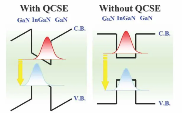
(29) 2.3 The quantum confined Stark effect in InGaN/GaN quantum well structure. In general, the InGaN/GaN QW LED has been grown on sapphire substrate in the [0001] orientation.. In. such. configuration,. the. [0001]. polar. axis,. resulting. from. the. non-centrosymmetric nature of the wurtzite phase, is aligned along the growth direction. (The different plane and orientation of hexagonal GaN is shown in Fig. 2.3.1) Hence, polarization discontinuities exist along the growth direction and create fixed sheet charges at surfaces and interfaces. Moreover, the InGaN layers have a tendency to grow pseudomorphically, resulting in an in-plane compressive stress due to lattice mismatch, which for InN/GaN is 11%. The existence of biaxial strain in the basal plane results in internal piezoelectric field normal to the QW plane. The total polarization of InGaN QW consists of spontaneous and piezoelectric polarization contributions.. These internal electric fields through the QW would tilt the potential band and lead to a spatial separate of electrons and holes in the QW, resulting a decreasing in degree of wave function overlap, which is called the quantum confined Stark effect (QCSE) and have been throroughly analyzed for InGaN/GaN QW [31][41][42]. (The schematic energy band diagram is shown in Fig. 2.3.2). This effect makes reduction in carrier recombination rate, red-shift of emission energy,. 14.
(30) and deteriorates the IQE for InGaN well widths exceeding 3-4 nm [23][32][42]. And the influences of QCSE will be deteriorated when QW width becomes more wide and/or content of indium increases. The QCSE can be waken by increasing injected carrier density, when carriers were injected more, the Coulomb screening of free carriers will occur, then, wake the internal electric field in QW, resulting in blue-shift of emission energy, increasing of recombination rate. And some groups introduced carriers into the structure by doping the QWs and/or barriers with Si, and effective screening of QCSE was observed [43][44].. In general, the blue-shift of emission energy with increasing excitation power density is generally ascribed to the combine of excition localization effect and screening effect of QCSE [23]. For lower excitation power density range, the carrier lifetime decrease with increasing excitation power density, and the dependence of emission energy on excitation power density was found to be nonlinear, which is explained by screening effect of QCSE. For high excitation power density range, the carrier lifetime is nearly constant, and the emission energy is linear excitation power density dependence, which is consistent with band filling effects. On the other hand, the QCSE will make the energy difference between the band-edge absorption and emission, which is called “Stokes shift”, which increases with increasing QW width and indium composition [30][32].. 15.
(31) Fig. 2.1.1 The DOS as a function of energy for different dimensions of structure.. Fig. 2.3.1 The different plane and orientation of hexagonal GaN.. 16.
(32) Fig. 2.3.2 The schematic energy band diagram for with QCSE and without QCSE.. 17.
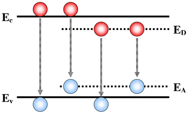
(33) Chapter 3 Experiment setup & Theory 3.1 Temperature dependent photoluminescence (PL). Photoluminescence spectroscopy is the optical measurement method to examine the quality and optical characteristics of material, it has the advantage of an un – contact and nondestructive. PL is the emission of light from a material under optical excitation. To excite the material to induce the emission, the energy of the excited light source should be higher than the band gap energy of the material. When the excited light is absorbed by material, electrons in the valence band would get the energy to jump into the conduction band then relatively produce a hole in the valence band. When an excited electron in an excited state returns to initial state, to comply with the energy conservation law, it will emit a photo whose energy is equal to the energy difference between the excited state and the initial state. But an excited electron also could be trapped by nonradiative centers, and no photon is induced.. If there are some defect energy level existed in energy band gap of semiconductor, they also could contribute to radiative recombination process. Therefore we could observe the multiple emission peaks in the PL spectra, and the intensity of the emission peaks is related to the contribution of the individual radiative recombination process. In general, there are four possible radiative recombination transitions in semiconductor (shown in Fig. 3.1.1). By analyzing the spectra of material, we can direct inspect the purity of material.. 18.
(34) On the other hand, temperature dependent PL is a useful method to extract the thermal activation energy of optical transition. The temperature dependent PL intensity is general expressed as: I ( 0). I (T ) = 1 + A exp(. − EA − EB ) + B exp( ) + ... kT kT. (3.1.1). where A, B is the coefficient related to defect density, and EA, EB is the activation energy. The activation energy is the physical value that means the transition energy barrier from radiative recombination to nonradiative reocombination, which can represent the exciton binding energy, localized energy, band offset of QW, energy difference between defect energy level to conduction band or valence band and …etc.. By plotting the Arrhenius plot for PL intensity, we can extract the activation energy to analyze the origin of radiative recombination. Moreover, temperature dependent emission energy and FWHM is also used to analyze the exciton localization effect in InGaN.. The setup of our PL system is shown in Fig. 3.1.2. The frequency doubled (2w) or frequency tripled (3w) beams of a mode-locked Ti : sapphire laser (w) pumped by Ar+ laser was used as pumping source. The wavelength of Ti : sapphire laser can be tuned from 700 nm to 900 nm, the pulse width is 200 fs. The repetition rate of the laser is 76 MHz. To direct examine the optical properties of InGaN/GaN MQW LEDs and avoid the absorption of GaN. 19.
(35) film, the pumping light source was a frequency doubled Ti : sapphire laser operated on 390 nm with 2 mW. After reflected by three mirrors, the laser light was focus by objective which focal length is 13.3 mm, to 0.05 mm in diameter and the luminescence signal was collected by the same objective. The probed light was dispersed by 0.55 monochromator (Jobin-Yvon Triax-550) equipped with 2400 grooves/mm grating. The resolution was controlled in 1nm by selecting 2400 grooves/mm grating and slit of 0.1mm. We use dichroic mirror to avoid the laser coupling with the PL spectrum. The PL was detected by a photo multiplier tube (PMT). For temperature dependent PL, the samples were mounted in a closed-cycle He cryostate, pump was used to draw out air in cryostate to obtain high vacuum (~ 10-3 torr), and temperature controller controlled the temperature from 15 K to 300 K.. 3.2 Temperature dependent time-resolved photoluminescence (TRPL). Time-resolved photoluminescence (TRPL) is an indispensable technique to study the dynamical process of photoexcited carriers such as relaxation, radiative, nonradiative, and localization processes. The transient luminescence intensity obtained by the data of TRPL is generally expressed by the following equation as a function of time after excitation: t I (t ) = I (0) exp( − ). (3.2.1). τ. where τ is the effective carrier lifetime, and can be extracted by fitting the experimental data by above equation. Moreover, the effective carrier lifetime can be expressed as below: 20.
(36) 1. τ. =. 1. τr. +. 1. τ nr. +. 1. (3.2.2). τ trans. where τ r , τ nr , and τ trans. are the radiative recombination lifetime, nonradiative. reocombination lifetime, and transfer time toward lower-lying energy levels. If radiative recombination occurs at the bottom of energy levels, the term of the transfer time can be neglected so that the equation is simplified as shown below: 1 1 1 = + τ (T ) τ r (T ) τ nr (T ). (3.2.3). On the other hand, the IQE can be written in terms of τ r and τ nr , where. ηint (T ) =. τ nr (T ) τ r (T ) + τ nr (T ). (3.2.4). Therefore, if we perform temperature dependent PL, and assume the IQE at the lowest temperature equals to 1, by equation 3.2.3 and 3.2.4 we can extract the radiative lifetime and nonradiative lifetime as a function of temperature. And by analyzing the relation between radiative lifetime and temperature, the dimensionality of nanostructure can be characterized.. Fig. 3.1.2 shows the experimental setup of the temperature dependent time-resolved photoluminescence. (TRPL). (Same. as. temperature. dependent. PL. setup).. Pulsed. photo-excitation for the TRPL was provided by the frequency doubled (2w) or frequency tripled (3w) beams of a mode-locked Ti : sapphire laser (w) which was pumped by Ar+ laser. The wavelength of Ti : sapphire laser can be tuned from 700 nm to 900 nm, the pulse width is. 21.
(37) 200 fs. The repetition rate of the laser is 76 MHz whose time interval is 13 ns. To direct examine the optical properties of InGaN/GaN MQW LEDs and avoid the absorption of GaN film, the pumping light source was a frequency doubled Ti : sapphire laser operated on 390 nm with 2 mW. The luminescence decay was measured with time correlated single photon counting (TCSPC) system in conjunction with monochromator using gratings whose grooves are 2400 grooves/mm. Time-resolution for the detection is about 4 ps. For temperature dependent experiment, the samples were mounted in a closed-cycle He cryostate, pump was used to draw out air in cryostate to obtain high vacuum (~ 10-3 torr), and temperature controller controlled the temperature from 15 K to 300 K.. 3.3 Micro-photoluminescence (µ-PL). Due to the progress of epitaxy technology and the understanding of quantum mechanics, low-dimension nanostructure such as nanorod, QDs has attracted much attention. Therefore, the measuring tool to probe such noanostructure is necessary.. In general, the focused laser. spot size of PL system is about 100 µm, it is not small enough to probe the properties of individual nanostructure such as nanorod or QDs, therefore, the µ-PL system has been developed. The µ-PL system uses optical objective to replace optical lens to focus laser light, with the minimum laser spot of 1 µm. By this system we can observe the optical properties of nanostructure, obtain higher excitation power density and scan the emission pattern of sample.. 22.
(38) Fig. 3.3.1 shows the setup of µ-PL system. The sample was excited by a He-Cd laser operating on 325 nm with 40 mW. First the beam of laser light was expanded by beam expander, and then focused into a spot with 1 µm in diameter on sample by 15x objective. The PL was collected in a fiber with 100 µm in the diameter and detected by a PMT or charge coupled display (CCD). Furthermore, µ-PL spectra were dispersed by a 320 nm monochromator (Jobin – Yvon Triax 320). The wavelength resolution is about 1 nm by using 300 grooves/mm grating and the slit of 0.1 mm. And position of sample can be controlled by piezo stage to scan the luminescence image of sample.. 3.4 Raman spectroscopy. Raman spectroscopy is a spectroscopic technique used to study the phonon modes of material. When laser light incident into the sample, photons will collide with atoms in material. For elastic collide, the energy of photon will not be changed, and the frequency of photon is same, this effect is called Reyleigh scattering. But for inelastic collide, the energy of photon will exchange with it of atom, then the frequency of photon will be changed, this effect is called Raman scattering. In the case of Stokes scattering, the photon losses energy. On the contrary is called anti-Stokes scattering. The diagram of the Stokes scattering and the anti-scattering is shown in Fig. 3.4.1. The Stokes scattering is usually much weak than the anti-Stokes scattering, so Stokes scattering is usually observed.. 23.
(39) Raman spectroscopy measures the change of photon energy called Raman shift (cm-1), which is expressed as below:. ∆σ = σ − σ ' =. ∆E hC. (3.4.1). where σ and σ ' are the energy of incident photon and scattering photon, respectively. From the Raman spectra, the phonon vibration modes, composition, stress, and quality of material can be study.. The Raman-active modes scattering efficiency is given by:. Sα ε s • χ • ε i. 2. (3.4.2). where ε s and ε i denote polarization for the incident and scattering light, respectively, and. χ is the Raman tensor of the scattering process. From above equation we can know the Raman active modes is related to the polarization, incident direction and scattering direction for incident and scattering light. Table 3.4.1 show the corresponding confiquration for GaN material. For a(b,c)d shown in Table 3.5.1, the a and d are direction for incident and scattering light, respectively. And b and c are polarization for incident and scattering light, respectively.. Fig. 3.4.2 shows the experimental setup schematically. The Raman scsttering was measured with an Ar-ion laser (Coherent INNOVA 90) as an excitation source with a wavelength of 488 nm. The scattered light was collected by a camera lens and imaged onto. 24.
(40) the entrance slit of the Spex 1877C. After reflected by two mirrors, the laser light was focus by a lens which focal length is 15 cm, and the scattering signal was collected into monochromator (Spex 1877C) by two convex lens. The probed light was dispersed by monochromator (Spex 1877C) equipped with 1200 grooves/mm grating. The Raman scattering is detected by cooling CCD with temperature of 150 K.. 3.5 Atomic force microscope (AFM). Atomic force microscope (AFM) images the surface of sample by scanning a sharp tip (10 µm in long and small than 10 nm in diameter) over and measuring the deflection of the tip. The fundamental setup of AFM is illustrated in Fig. 3.5.1. A piezoelectric controller moves the sample in x-y direction under the tip. The position of the tip is measured by reflecting laser from the backside of the cantilever to a split photodiode. Depending on the distance between the tip and the sample so that the force acting on the tip is repulsive, the AFM work in contact mode. In non-contact or taping mode the tip is further away from the sample and in the region of an attractive force [70]. The cantilever is set to vibration close to its resonant frequency and change in the surface morphology lead to changes in the frequency, which can be measured sensitively.. 3.6 High resolution X-ray diffraction (HRXRD). X-ray diffraction is a non-destructive method to study the structural properties of 25.
(41) material, which can be used to judge the crystal quality, thickness and the composition of compound semiconductor. And the degree of lattice mismatch between an epitaxial layer and the substrate also can be charactized. XRD utilizes two successive Bragg reflections from two independent crystal planes. From Bragg’s law, the condition for constructive interference is:. 2d hklc sin θ B = nλ. (3.6.1). where dhklc is the reciprocal lattice spacing and can be expressed as. 1 d hklc. =. 4 h 2 + hk + k 2 l2 ( ) + 3 a2 c2. (3.6.2). where a is the crystal lattice constant, (h, k, l, c) is known as the Miller indices of the plane,. θ B is the incident angle, n is an integer representing the diffraction order, and λ is the wavelength of the incident radiation. For a fixed incident X-ray wavelength λ, each crystalline material has a characteristic X-ray diffraction pattern associated with it, which yields a accurate information on its crystal structure and lattice space. The ω, ω-2θ scan and reciprocal space mapping (RSM) measurements of high resolution x-ray diffraction (HRXRD) made with a Philips MRD X’pert PRO diffractometer using CuKα1 radiation were applied to analyze the crystal quality and strain in InGaN QW.. 26.
(42) Ec ED. EA. Ev Fig. 3.1.1 Radiative recombination transitions in semiconductor.. Fig. 3.1.2 Setup of temperature dependent PL and TRPL system.. 27.
(43) Fig. 3.3.1 Setup of µ-PL system.. Fig. 3.4.1 The diagram of the Stokes scattering and the anti-Stokes scattering. 28.
(44) Table 3.4.1 Selection rules of wurtzite structure. Fig. 3.4.2 Setup of Raman system.. 29.
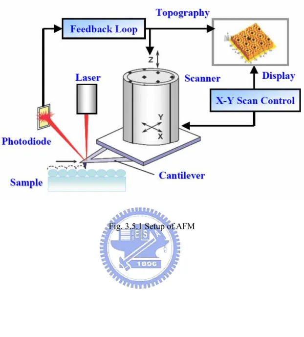
(45) Fig. 3.5.1 Setup of AFM. 30.
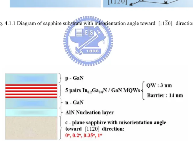
(46) Chapter 4 Optical properties of InGaN/GaN multiple quantum well light emitting diodes grown on sapphire substrate with different misorientation angle 4.1 Introduction. Generally, GaN-based optoelectronic devices grown on c-plane (0001) sapphire substrate, but due to the large mismatch of lattice constant between GaN and sapphire, huge density of threading dislocations up to 109 cm-2 present in nitride layers, deteriorating the surface morphology and crystal quality of GaN and InGaN active layers. To obtain high-quality LDs, a highly uniform and smooth surface of the expitaxal GaN film is required, because surface macrostep patterns sometimes produce a large propagation loss. Surface morphology of the epitaxial GaN film depends on various growth conditions, such as nitridation of the substrate [45], growth conditions of the buffered layer [5][46], ramping conditions before GaN epitaxial growth [47][48]. Some groups have studied the influences of using sapphire substrate with slight misorientation toward [11 2 0 ]. direction on growth of GaN. [14][15][16][17]. (Diagram of sapphire substrate with misorientation angle toward [11 2 0] direction is shown in Fig. 4.1.1) From AFM and XRD results, they found that the surface macrostep patterns of GaN greatly depend on the slight misorientation angle of the sapphire substrate. Moreover, the improvement of the crystal quality and the surface morphology of GaN by using slight misorientation angle have been observed. T. Yuasa et al. proposed these are due to appropriate atomic steps of the substrate formed by the slight misorientation, then 31.
(47) relieve the lattice mismatch between GaN and sapphire [17]. However, the optical properties of InGaN MQW LEDs grown on sapphire substrate with different misorientation angle have not been studied so far. The influences of misorientation angle on optical properties of InGaN QW are still unclear.. In this work, the optical properties of InGaN/GaN LED using sapphire substrate with misorientation angle of 0o, 0.2o, 0.35o and 1o toward [1120] direction have been studied. From temperature dependent PL measurement, the anomalous emission energy shift as function of temperature, which is so-called S-curve, has been observed [18]. By using Eliseev et al. proposed model [19], the degree of potential fluctuation of the InGaN as function of misorientation angle has been characterized. Moreover, the recombination dynamic of carriers and the dimensionality of nanostructure in active region have also been studied by temperature dependent TRPL measurement.. On the other hand, the material properties of samples have been investigated by atomic force microscope (AFM), high resolution transmission electron microscopy (HRTEM), high resolution X-ray Diffraction (HRXRD) and Raman spectroscopy.. 4.2 Sample preparation. The sample structure in this study is shown in Fig. 4.2.1. The InGaN/GaN MQW LEDs in this work were grown by a commercial LP-MOCVD system with a vertical reactor. The 32.
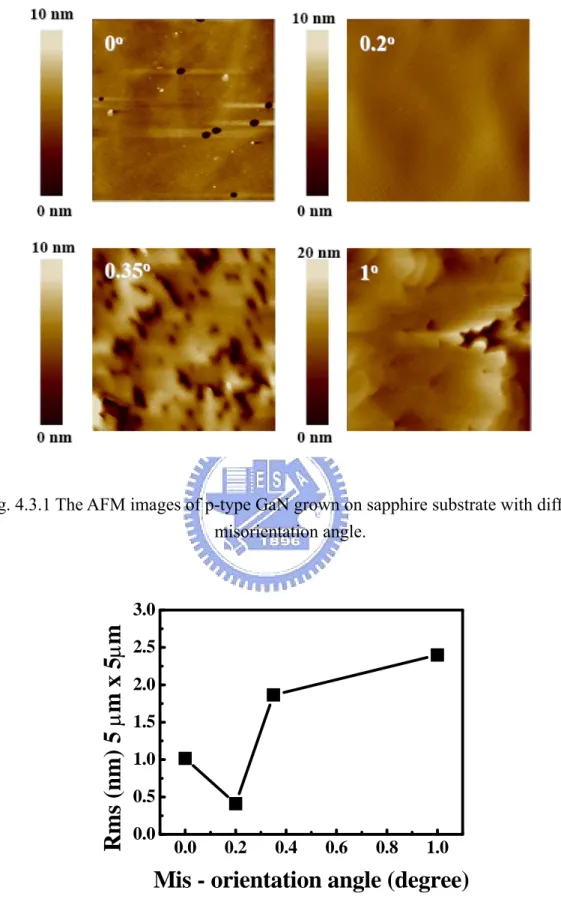
(48) MO compounds of TMGa, TMIn, TMAl and gaseous NH3 were employed as the reactant source materials for Ga, In, Al and N, respectively, and H2 and N2 were used as the carrier gas. All samples were grown on c-plane (0001) sapphire substrate with different misorientation angle of 0o, 0.2o, 0.35o and 1o toward [11 2 0] direction, consisting of 50-nm-thick AlN nucleation layer, a 3.5 µm Si-doped n-type GaN, and an unintentionally doped active layer with InxGa1-xN/GaN MQWs, and 0.4 µm Mg-doped p-type GaN. The doped concentration of n- and p-type GaN is nominally 5 x 10¹⁸ and 1 x 1019 cm-3, respectively. For conventional MQW LEDs, the MQWs layer comprise six periods In0.2Ga0.8N well (~ 3 nm) and GaN barrier (~ 14 nm).. After epitaxial growth, the fabrication of devices was carried out as follows. First, the top ohmic contacts of In0.2Ga0.8N/GaN MQW LEDs were formed using a metal system of Ni/Au for p+-GaN contact layer. Next, Ti/Ai systems were evaporated onto the exposed n-GaN epilayer. Finally, In0.2Ga0.8N/GaN MQW LEDs were cut into square pieces with the dimension of 300 × 300 µm2.. 4.3 Material properties of InGaN/GaN MQW LEDs 4.3.1 Atomic force microscope image. The AFM images (5µm x 5µm) of the p-type GaN are shown in Fig. 4.3.1 and the root mean square (RMS) of surface roughness measured by AFM is shown in Fig. 4.3.2. From. 33.
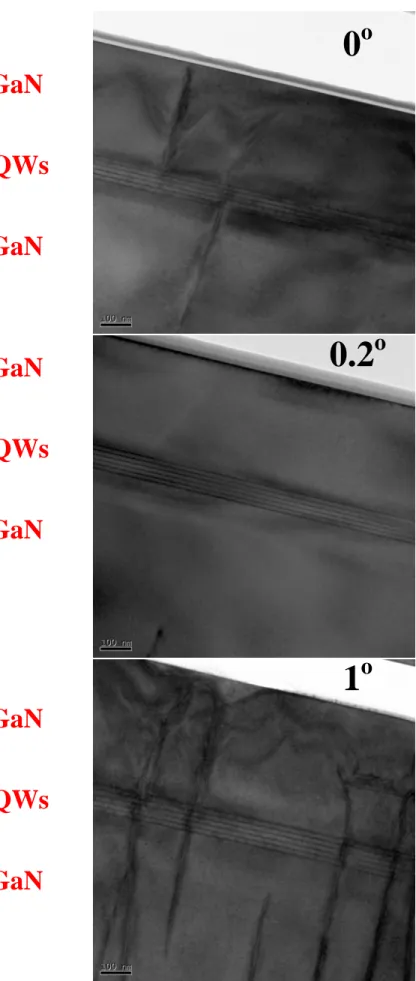
(49) images we can observe that the surface morphology becomes smoother as misorientation angle increases from 0o to 0.2o, but it is deteriorated as misorientation angle increase above 0.2o. Moreover, except the 0.2o sample, we can see some pits formed in p-type GaN and become more deteriorative in the angle above 0.2o. The formation of pits on p-GaN is due to large dislocation density produced from underlying layer. The pits will degrade the surface morphology and causes rough surfaces with higher RMS values.. 4.3.2 High resolution transmission electron microscopy. In order to observe the homogeneity of InGaN/GaN MQWs and the dislocation density in the device, the structural analysis was performed by means of cross-section HRTEM. Fig. 4.3.3 is the cross-section HRTEM observation of the LED grown on sapphire substrate with misorientation angle of 0o, 0.2o and 1o. The n-type GaN, p-type GaN and six QWs can be clearly identified in the images. For 0o and 1o sample, we can see that many dislocations produced from underlying GaN layer penetrate through the InGaN/GaN MQWs and reach upper p-type GaN layer. The dislocation density extracted from TEM image is shown in Fig. 4.3.5. By using misorientation angle of 0.2o, the producing of dislocations is suppressed and the quality of device is improved. About its origins, some articles have proposed that the growth mode of GaN will be shifted from spiral-dominated to step-flow as sapphire substrate with slight misorientation angle about 0.2o [16]. From Burton, Cabrera and Frank (BCF). 34.
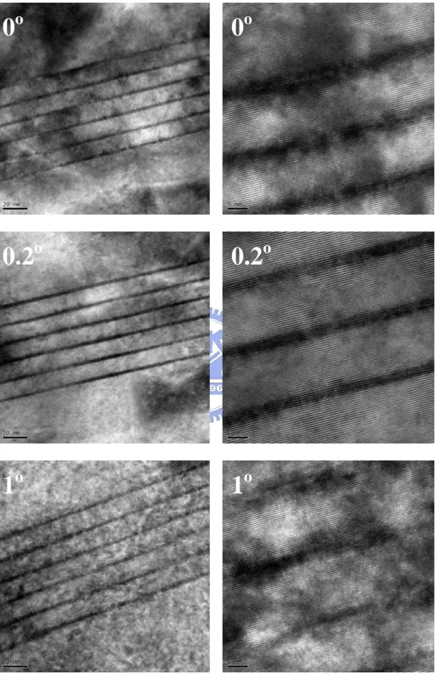
(50) theory, spiral growth is dislocations controlled, and it competes with step flow growth on a misorientation substrate [53]. The condition for spiral annihilation can be simplified to:. ω MC < ω S. where ω MC. (4.3.1). is the misorientation terrace width which decrease with increase of. misorientation angle; ω S is width of the terrace on the two interlocking spiral ramps that create a spiral hillock in GaN. When the misorientation angle increases to satisfy the above condition, the misorientation step would annihilate the spiral steps faster than the spiral could spread on the surface. Therefore, due to suppression of spiral growth, the GaN grown on misorientation angle of 0.2o can effectively decrease dislocation produced in underlying GaN layer. On the other hand, the incorporation of group III atoms, the epitaxial growth of III-nitrides, is closely related to the density of dangling bonds at step edges [72]. Therefore, when the misorientation angle is too large, the density of step edges is too high and it becomes difficult to grow with smooth surface, and the strain relaxation in the interface increases, resulting in increasing of dislocation density.. The Fig. 4.3.4 shows the HRTEM images for three samples, the six pairs InGaN/GaN QWs are clear observed, and the well and barrier layer thickness are estimated to be about 3 nm and 14 nm, respectively. In the detailed structure of the MQWs, a lot of dark spots are observed in the wells, the diameters of these dark spots are about 5 nm. This dark spots have. 35.
(51) been observed for several articles [26][68], which is the indium-rich clusters due to large discrepancy in atomic size between indium and gallium and the large lattice mismatch of 11% between InN and GaN. Besides, we also could see that thickness fluctuation existing in MQWs. And from figure we can see the composition and thickness homogeneity of MQWs is improved as miorientation angle increases from 0o to 0.2o, but it deteriorated as misorientation increases above 0.2o. There are many reports said that indium incorporation is dislocation sensitive [54][71]. From Fig. 4.3.3, the dislocations penetrating through the InGaN/GaN MQWs structures could significantly increase the indium compositional fluctuation around the dislocation. The presence of dislocation in the underlying MQW layer strongly effects the indium incorporation into the upper MQW layers. Moreover, the indium incorporation is also significantly sensitive to the surface morphology of an underlying layer. The article indicates that the indium incorporation efficiency is drastically higher on the facets than on a smooth surface [55]. The deposition of the indium atoms is attracted at facets rather on a smooth surface to reduce the surface energy due to many dangling bonds at facets. Therefore, the indium phase separation in InGaN QWs layer can easily occur on the rough surface of epilayer. The dislocations will also degrade the surface morphology and cause rough surface with higher RMS values. Therefore, due to fewer dislocation and smoother surface of underlying GaN layer for 0.2o sample, the. 36.
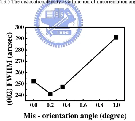
(52) homogeneity of InGaN/GaN MQWs is improved.. On the other hand, the dislocations penetrate into p-type GaN will degrade the surface morphology and cause rough surfaces with higher RMS values, which may result in a depletion of Mg from the surface and cause a reduced doping level, deteriorating the contact resistant for InGaN/GaN MQWs LED [56][57]. Moreover, the high dislocation density will induce anomalous high leakage current, then, the performance of LED is degraded [69].. 4.3.3 High resolution X-ray diffraction. HRXRD rocking curve (XRC) measurement for symmetrical GaN (002) reflections was applied to evaluate the crystal quality of GaN thin films. The FWHM of XRC for GaN (002) was plotted as shown in Fig. 4.3.6. We can observe that the FWHM is decreased as misorientation angle increases from 0o to 0.2o, but it increases as misorientation angle increase above 0.2o. The FWHM of the symmetrical GaN (002) is correlated to the threading dislocations density [49]. Therefore, it is ascertained that dislocation density tends to decrease as sapphire substrate with slight misorientation angle about 0.2o, but the crystal quality is deteriorated as misorientation angle increases above 0.2o, which is agree with our HRTEM analysis results. Fig. 4.3.7 shows the HRXRD ω-2θ diffraction pattern for the LEDs with misorientation of 0o, 0.2o, 0.35o, and 1o, respectively. As can be seen, the HRXRD diffraction pattern shows. 37.
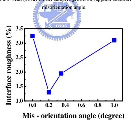
(53) one periodical structures, which can be attributed to the In0.2Ga0.8N/GaN MQWs. In addition, the third order satellite peak of the diffraction pattern for all samples can be clearly observed, suggesting that the grown structure has sharp interfaces and good periodicity between GaN barrier and InGaN well. Additionally, the inset shows the variation of MQWs interface roughness (IRN) with misorientation angle of sapphire substrate. The interface roughness value of MQWs can be obtained from the following equation [63].. 1 2. Wn = W0 + (ln 2) n∆θ M ⋅. σ. (4.3.2). Λ. where n is the order of the satellite; Λ and σ/Λ are thickness of the period and IRN, respectively; ∆θM is the angle distance between adjacent satellite peaks; W0 and Wn are the FWHM of zeroth- and nth-order peaks, respectively. The results are shown in Fig. 4.3.7. From figure we can found that IRN of InGaN/GaN MQWs decreases with increasing misorientation angle of substrate, and reaches minimum which is about 1.35% for 0.2° misorientation sapphire substrate was used. Increasing the misorientation angle to 1° increases the IRN of MQWs. The previous reports indicated that the IRN of MQWs is affected by defect, microstructure and phase separation in MQWs [63]. Based on x-ray analysis, we can prove that the defect density of 0.2o sample is lower than other samples, and can also concluded that defect density of 0.2o sample was reduced dramatically, which are consistent with the results observed from HRTEM images.. Fig. 4.3.9 shows the RSM results for InGaN/GaN MQW LEDs grown on (a) 0°, (b) 0.2°,. 38.
(54) (c) 0.35° and (d) 1° misorientation sapphire substrate, respectively. The diffraction pattern was obtained from the asymmetric (1 0 1 5) reflection of the GaN epilayer. Compared with sample 0o, 0.35o and 1o, the reciprocal lattice point (RLP) of GaN layer of 0.2o sample is circular, indicating that the spread of RSM intensity for 0.2o sample is narrower than that of RSM intensity for other samples. In general, the spread of diffraction intensity is related to the orientation distribution and decrease in the coherency of the scattering along the structure [64]. The asymmetrical feature for RLP of GaN indicates the out-of-plane lattice mismatch formed in GaN layer. This means that the GaN epilayer grown on 0.2° substrate has better crystallization quality. Besides, the RLP of satellite peaks can be clearly observed for 0.2o sample and the satellite peaks up to four orders, while the reciprocal lattice point of satellite peaks became relatively weak for 0o sample and 0.35o sample or vanished for 1o sample, suggesting that the InGaN/GaN MQWs of good quality were grown. Therefore, based on the above-mentioned results, the crystalline quality of 0.2o sample is relatively good in contrast to the quality of other samples, and the noticeable improvement in the quality of GaN epilayer could be responsible for achievement of high quality InGaN/GaN MQWs.. On the other hand, the overall strain state of MQWs with respect to the GaN epilayer can be examined by RSM. S. Pereira et al. proposed the method to investigate the strain and composition distributions within wurtzite InGaN/GaN layers [50]. The information can be extracted from the elongation of broadened RLP in asymmetric x-ray reflections. The. 39.
數據

+7
相關文件
S15 Expectation value of the total spin-squared operator h ˆ S 2 i for the ground state of cationic n-PP as a function of the chain length, calculated using KS-DFT with various
We investigate some properties related to the generalized Newton method for the Fischer-Burmeister (FB) function over second-order cones, which allows us to reformulate the
Nowadays Nan-Gan Island and Bei-Gan Island are in Matsu archipelago called Gan-Tang-Shan by Ming Dynasty. Gan-Tang-Shan located on the sea out Min-Jiang estuary in Fu-Jian Province
電機工程學系暨研究所( EE ) 光電工程學研究所(GIPO) 電信工程學研究所(GICE) 電子工程學研究所(GIEE) 資訊工程學系暨研究所(CS IE )
Li, Shaoting Zhang, Xiaogang Wang, Xiaolei Huang, Dimitris Metaxas, “StackGAN: Text to Photo-realistic Image Synthesis with Stacked Generative Adversarial Networks”, ICCV,
GaN transistors with high-power, High temperature, high breakdown voltage and high current density on different substrate can further develop high efficiency,
Several methods that modulation effective work function to maintain p-type gate material is the direction of future research, sush as microwave annealing with plasma
本研究在有機物部分,除藉由螢光光譜儀進行螢光激發發射光 譜圖(Excitation emission fluorescent matrix,
