Novel low-stress SjO2-F film deposited by
room-temperature liquid-phase deposition method
Ching-Fa Yeh and Shyue-Shyh Lin
Department of Electronic Engineering, National Chiao Tung University, 1001 Ta Hsueh Road, Hsinchu, Taiwan, Republic of China
.
ABSTRACT
To develop a low-stress thin film for micromachined devices, a novel liquid-phase
deposition (LPD) SiO2xFx technique utilizing silica-saturated H2SiF6 solution with H20addition only is proposed. Due to extremely low-temperature processing and fluorine
incorporation, the stress of the LPD SiO2x Fx film can be less than 100 MPa. In this paper, we found that the deposition parameter of H20 addition has much effect on the stress ofas-deposited LPD oxide. The stress variations with thermal cycling has also been clarified. We
found that the LPD SiO2-xFx film will be a good candidate as low-stress film for
micromachined devices.
Keywords: low-stress, liquid phase deposition, SiO2xFx
1. INTRODUCTION
The output characteristics of many micromachined and microfabricated devices are largely dependent on the mechanical stress of their 1 For example, in surface-micromachined sensors, the mechanical stresses are responsible for large bending, warping,
and even fracture of thin film materials. Therefore, only low-stress thin films can be used in
surface-micromachined devices. However, most thin films deposited at low temperature
(300°C — 600°C)
still have large residual stress (200 MPa 300 MPa).2'3 Thus, it is an
important issue to develop a low-stress thin film for the micromachined and microfabricated devices.
Recently, a new oxide formation technology using the liquid phase deposition (LPD)
method has been developed.4 There are two main advantages for LPD SiO2.xFx in
comparison with other oxides. First, the substrate temperature during deposition can begreatly reduced to room-temperature. Since LPD oxide can be deposited at room-temperature,
its stress is less than 100 MPa. Second, the fluorine atoms can be naturally incorporated into
LPD oxide. These strongly suggest that LPD oxide technology is a potential candidate for
applying to micromachined and microfabricated devices.
Until now, the detailed properties about the stress of LPD SiO2xFx was still unknown. In this paper, we will first investigate the influence of deposition parameter on the stress of LPD oxide. Because the change in LPD oxide microstructure with heat treatments often
results into drifting in mechanical stress, next, the stress variation in LPD oxide with different thermal cycling will also be clarified.
2. EXPERIMENTAL METHODS
In preparing the aqueous solution for LPD oxide formation, 75 g of 99.99% pure silica (Si02) powder was added to 1750 ml of 4 mol/l hydrofluosilicic acid (H2SiF6). After being
stirred at 23°C for 17 hours, the solution became saturated with silicic acid [Si(OH)4]. Then
the solution was filtered to remove the undissolved silica powder. To further make the
solution become supersaturated with silicic acid for deposition, the deionized water (H2O)ranged from 250 ml to 750 ml was added to the 1000 ml saturated solution.
P-type, (100), 10 20 1-cm, 4-inches silicon wafers were used as substrates in this
experiment. The thin native oxides, naturally formed on the substrate surfaces in the HC1 +H20 + H2O2 mixed solution during initial cleaning, were reserved for LPD oxide deposition. The deposition temperature of 25°C was accurately controlled by a water bath. The thickness of LPD Si02-xFx was controlled by immersing time.
LPD Oxide stress was determined through measuring the radius of wafer curvature with a
Tencor FLX-2320 thin film stress measurement instrument using a single laser reflection technique.5 After deposition, the oxide layer on the back side of wafer was stripped using a
6:1 buffered HF solution. For each sample, the radii of wafer curvature were measured prior to LPD oxide deposition and following such deposition. The stress (cs) can be calculated from the changes in the radius of wafer curvature according to the following equation:
E .().(I_I)
(1)6(1—vs) t1
R2 R1where Es and v are the Young's modulus and Poisson's ratio of Si, tf and t are the thickness
of LPD oxide and Si wafer, R2 and Ri are the radii of wafer curvature with and without LPD oxide.
The measurement of in-situ thermal-cycling stress measurement was performed with the above instrument. The stress instrument has additional arrangement in which a wafer with the
deposited oxide can be heated in an N2 atmosphere to the required temperature at a preset ramp rate (8.5°C/mm), and then cooled to room temperature at a maximum cooling rate of
1 .6°C/mm. During heating and cooling, the stress was measured periodically.
In the measurement of ex-situ thermal-cycling stress, post-deposition heat-treatments
were performed at 300 800°C in N2 ambient for 1 hr. The wafer curvature was immediately measured after each of the heat-treatments. After the measurements of ex-situ thermal-cycling
stress were completed, the oxide film was stripped from the substrate, and the bare wafer curvature was measured again to check whether plastic deformation of the silicon substrate
occurred in the processing steps.7' 8
3. THIN FILM STRESS
In general, the total stress (CT) in thin film has two components, they are thermal stress
(th) and intrinsic stress (cj). That is,
Tthin
(2)The thermal stress component is attributed to that the difference in thermal expansion coefficients between the film and the substrate can cause differential contractions during
cooling from the deposition temperature. Gth can be given by9
h E1 I (1 —
v1)J
(a —
a)dT,
(3)where Efis the Young's modulus of the film, vfis the Poisson's ratio of the film, as and aare
the thermal expansion coefficients of the substrate and the film, respectively, and Td and Ta
are the deposition and the stress measurement temperature, respectively. For Si02 on Si, Ef/
(l-Vf) = 8.5 x 10¹¹ dynes/cm2. If it is assumed that a5 and
Lf do not change with
temperature, then the above equation can be simplified to
E
f)(afs)(Td—Ta),
(4)1— Vf
since as is larger than affor oxide film on Si,'° and Td is usually larger than Ta, the resulting thermal stress at room temperature becomes compressive. The intrinsic stress in the oxide film
is caused owing to the bonds structure (bonding between Si, 0, and OH). It can be either
tensile or compressive.
4. RESULTS AND DISCUSSION
Fig. 1 shows the dependence of stress on H20 quantity for the wafers with 320 nm-thick LPD SiO2-xFx. All the stresses were found to be in a state of tensile, and the magnitudes were
in the range of 70 120 MPa. These values are much lower than that of 200 500 MPa in
CVD 1 1-15 Since the deposition and the measurement temperatures are nearly the
same, the stress mainly results from intrinsic stress. The intrinsic stress in LPD oxide results from the bond strains originating from the dehydration reaction during deposition. When the
Si-O-Si bonding takes place after dehydration, there must be a large puckering 1 6 If
sufficient energy is not applied to the oxide, bond strains remain and result in intrinsic stress.
Since dehydration reaction causes shrinkage of the film, the intrinsic stress should be
tensile. 17
The 320 nm-thick film deposited with 250 ml H20 shows a stress of 72 MPa, but both the same-thickness films deposited with 500 ml and 750 ml H20 show a rising stress to 112
MPa. In our previous studies,6 we have shown that the fluorine atoms can be naturally
incorporated into the LPD oxide during deposition. And the less the H2O quantity added, the
more the fluorine atoms incorporated into the LPD oxide. Thus, for the film deposited with
250 ml H20 the lower stress (72 MPa) can be attributed to the more fluorine incorporation in
the film. This is consistent with the hypothesis that fluorine incorporation results in strain
l 820 The interaction between a fluorine atom and a strained Si-O bond will
generate a Si-F bond and a nonbridging oxygen bond, and result in a local strain relaxationand thereby a stress reduction.21
According to the above discussion, the stress of LPD oxide prepared with 750 ml H20 added should be larger than that prepared with 500 ml H2O added because of less fluorine atoms incorporated in the former. However, in Fig. 1 ,we found that there is only a little
difference in stress between the two samples. For LPD oxide prepared with 750 ml H2O, the less increase may be due to more OH contained in the film.22' 23 After H20 has been added
to a saturated H2SiF6 solution, the intermediate polysilicic acids will be formed by the
polymerization of the silicic monomer Si(OH)4, and then absorbed onto the substrate
surface.6 Acid-catalytic dehydration occurs between these absorbed polysilicic acids,
followed by Si-O-Si bond formation. The larger the H20 quantity added, the faster the
polysilicic acid formed and absorbed onto the substrate surface. In that case, the dehydration
reaction cannot be completely finished in time, and a large amount of residual Si-OH bonds remain in the film, thus make stress less increase.
The effects of in-situ thermal cycling on the total stress for LPD oxide were measured and shown in Fig. 2. During the heating, the total stress tends to become more tensile with
increasing temperature. During the cooling, the total stress becomes less tensile with
decreasing temperature. The final value of total stress is larger than the initial value, and the total stress variation shows a hysteresis. As mentioned above, a total stress in thin film during thermal cycling includes two components: thermal stress and intrinsic stress. According to Eq.
(4), the thermal stress will show a linear relationship with temperature. With increasing temperature, the thermal stress will become more tensile. However, during the cooling, the thermal stress will become less tensile. If there is no intrinsic stress, the variation of total stress during thermal cycling should follow the linear variation of thermal stress only, and show no hysteresis. However, from the hysteresis as shown in Fig. 2, it is believed that the
LPD oxide has some amount of intrinsic stress.
The variation of intrinsic stress during the thermal cycling is determined by the changes in the oxide structure, especially the escape of OH, formation of additional Si-O-Si bonds, and then reconfiguration of these bonds. The annealing at a higher temperature will promote the
escape of OH out of LPD film and the formation of Si-O-Si bonds. As mentioned in the
handbook,'6 the Si-O-Si bonds formation can give rise to a large amount of bond strains. If a
bond strain is not relieved, it will result in an intrinsic tensile stress in the film. Therefore, with increasing temperature, an increasing tensile intrinsic stress is developed in the oxide,
and the total stress becomes more and more tensile. If a large intrinsic tensile stress is left in
the film at the beginning of cooling, it will remain constant with decreasing temperature.2
Thus, the total stress variation during the cooling exhibits larger than that during the heating, and a hysteresis occurs.
Fig. 3 shows the dependence of total stress on temperature in the case of ex-situ thermal cycling for the LPD oxide (234 nm) deposited with 250 ml H20. After an ex-situ annealing at 600°C, the total stress can drastically decrease from 80 MPa (tensile) to 4 MPa (compressive). The figure shows great difference in comparison with that of the sample with in-situ thermal cycling. To study the relationship of stress variation with the bonding structure, the variation of intrinsic stress (gin) with temperature, as shown in Fig. 4 was obtained by subtracting the
calculated thermal stress (y)fromthe total stress
The increasing of intrinsic stress after 1 hr thermal annealing in —300°C is due to the
escape of OH and reconfiguration of structure bonds as mentioned previously. However, after
annealing at a higher temperature (400°C 600°C) the intrinsic stress decreases a little. This
is not only because the high-temperature annealing can make the silicon and the oxygen atoms
in the oxide restructure and thereby result in reconfiguration of the Si-O-Si bonds, but also
will relieve the bond strains and decrease the intrinsic tensile stress.3 Therefore, there seems to exist a threshold temperature (400°C), beyond which the tensile intrinsic stress of the film
will decrease. If the annealing temperature is over 600°C, we found that the intrinsic stress
tends to become more tensile again. It can be attributed to the removal of fluorine atoms in the
film owing to high-temperature annealing. As discussed above, the removal of fluorine will
make strain bonds relaxation disappear and resultantly increase intrinsic stress. Fig. 5shows
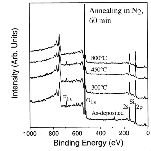
the typical XPS spectra for the annealed LPD oxides at different temperature. The
disappearance of Fls peak indeed confirms that the annealing at 600°C 800°C has removed
the fluorine atoms from the film.
5.CONCLUSIONS
A novel low-stress LPD 51O2-x Fx technique utilizing silica-saturated H2SiF6 solution
with H20 addition only has been developed. The stress of as-deposited LPD SiO2.x Fx film
is tensile, and can be less than 100 MPa because of low-temperature processing and fluorine
incorporation. If an LPD oxide is deposited with less H20 quantity, the film stress can
become much lower due to more fluorine atoms incorporated in the film. A hysteresis
phenomena of stress can be observed for the LPD oxide with in-situ thermal-anneal cycling. In the case of ex-situ thermal annealing, the intrinsic stress will increase owing to the removal of OH (—300°C)and the removal of F (> 600°C), but will decrease owing to the strain bonds relaxation (400°C 600°C). The stress can decrease as low as 4 MPa (compressive).
6. ACKNOWLEDGMENT
This study was supported by the National Science Council, Republic of China, under
contract number NSC 85-221 5-E-009-057.
7. REFERENCES
1. 5. M. Sze, 'Semiconductor Sensors," John Wiley & Sons, Inc., 1994.
2. K. Rarnkumar and A. N. Saxena, J. Electrochem. Soc., vol. 139, p. 1437, 1992.
3. K. Ramkumar, S. K. Ghosh, and A. N. Saxena, J. Electrochem. Soc., vol. 140, p. 2669,
1993.
6E9Z Ion !dS/OQE 9L6T
':
d'L
10A 'AOJVD'I
'Joqsij •M •V p1113'oquqD
•'-I •D'uJN
•A
•:z
0L6T 'cTTc d'jj
10ASiq
iddV
I
'OS
•N PU1 'qo:ijA
'!u11UnSH
.ZZ 686T 'Tt'T d'at
10A'11J
3TAOU U0JIOOLEI EEEI '1J,4Id
•I
PU1'PNJ'
•{
'pIEflh1M M '!1'IOA
'fl'IO
N
'OJqSTN
A
L86T '06TI
d
'j
10A'S
J0I0flN SU1Jj[J[
'J,ft
d
L
P"
'1OtqSTN A'AsP
J
[
066T'
d
'TI
'bA
'J2O'J
OTAU •UoJ1oTI 1EEII'MoIZ
•D•I
PU1'0HH
•tI •'I 'sTu1qT!MI,\Jd
•N 6T .I
661 'ZcLT d'gj
10A'0S
woqooi:io
f
'UTpOo3Eff
pu
'&nnq
9
f
'SOSAflONU
'SI 9861 'L91 Id
'oun
'oouqooj
pU
oou!oS
S'P!I0S
"305 WOqOOJIOOf
'T)J1
{
pui
'M1ZU1{ }J 'JflTflE)pN 1AI LT 086T '°Duiqsijqnd
'g9d
'E'bA
'JOflp[ 'SSOJft 'S'1
'SJO1OnPUOOTUJS UO)ooqpu
'ppo
'Vi
pu
V
'91S6T
'19oc d'jç
'i0
"Siq
idd
'1'MnIH
•DcI
S6T
'zzT d 'S6T-ZS6T 'oouo!3S JOsuoi2oqddy
'Jqi
f
pui
'rJusoo{
'
'zosmf'j,
jT cS6T '0c6d
'ZT
'bA'°°S
•TUOITOOJ:l3TJ '1 'UTIPUOM •tI 'H'd
'I
U1
/c)Isu!Iows•o
':j
986T 'VD'q:1
sUng
'SSOJd°!W'1
'1 I°A';io
ISTEAP
TOJ UJSSOOOJd UO3tJ5'Joqrrn
'Ni
pui
jo
g66T
't'9c
d
'Ot'T IOA '•O0S•woqoouoo[
'1'PUThH
'A PUE 'SJO2I1M'N
'U!1UflOd'0
0
'UUJSTOJV'oidui
'U '11 '0661 '8901 d 'SH 'bA'Ouqoo
PS
'A
f
'11I,10D'f
P
'd
'S''H
'H '01 '9861 'L91i
'd
'SET 'bOA "OOS 'UxoqoOJ2ooI
'!PS
{
pu
'A\ZU1){J
'N
'6 '1661'8TT
'd
'8T
'JOA"OO
inoqoOnoj
f
'U1U1ST) '\TprJ
JOqS)Jfl
'PA '8 '0661'oj
'd '61 'bOA"N
'UOJ3O13'f
'U1UIST)'
pu
JoqS3iflij 'PA L 'i66T 'LLT E 'd 'Jj7J 'bOA"30
'UJoq3OJ1oo'f
'UT
'H'0
'Ut'3
'J
'J
'1A
'ti 'D 9 '6861'j
'd'9T
'bOA"O0
UJt[OOJPOI'f
'
1fl1tJH 'N'd
pU13 'U1T1IS!O)J '\T ')J31NN
TI'c
't'66T 'ELT'd
'Tip 10A 'SOJAOQUOJ13
''L
EIEI
'UA
D 'AU1
'uqj
'TI'J
'U1A
'Z
'I
''fl
S 'S 'EPAJ
'::) '170
(I) C,)(I)
0
Cl) Cl) 'ZD:•
C')Temperature (°C)
Fig. 2. Variation of total stress for LPD oixde during in-situ thermal cycling.
SPIE Vol.2639 /301 120 110• 100-
90-80
70—
- I I I 200300
400
500
600
700
800
H20
Quantity (ml)
Fig.
1. Dependence of stress on H20 quantity for 320 nm-thick LPD oxides
H2SiF6 =
1000
ml
400
300
200
100
0 H2SiF6 : H20 =1000
ml: 250
ml
Thickness =321.4
nm
.t
•••.
D .__øøø'• •...
.
Heating• Cooling
0
100
200
300
400
500
302/SPIE Vol. 2639
300'
Annealing in N2, 60 mm
H2SiF6
:H20
=
1000
ml : 250 ml-%
200 'Thickness
=
234
nm
(TiTotal
Stress -100• • I • I • I • I 0200
400
600
800
1000
Annealing
Temperature (°C)
Fig.
3. Effects of ex-situ thermal annealing temperature on total
stress for 234 nm LPD oxide.
300
200
/
•
.Intrinsic
Stress
0 Annealing in N2, 60 mm
H2SiF6 : H20 =
1000
ml: 250ml
Thickness=
234
nm
-100
I • I • I I 0200
400
600
800
1000
Annealing
Temperature (°C)
Fig.
4. Effects of ex-situ thermal annealing temperature on
(1)
>
U) ci)
—
Fig.
5.
XPSspectra for LPD oxides with ex-situ thermal
annealing at different temperature.
SP!E Vol.2639 1303