1150 IEEE TRANSACTIONS ON CIRCUITS AND SYSTEMS—II: EXPRESS BRIEFS, VOL. 54, NO. 12, DECEMBER 2007
Fast-Transient DC–DC Converter With On-Chip
Compensated Error Amplifier
Ke-Horng Chen, Hong-Wei Huang, and Sy-Yen Kuo, Fellow, IEEE
Abstract—A fast-transient dc–dc converter with on-chip
com-pensated error amplifier is presented in this paper. The error amplifier uses three transistors and one voltage follower to imple-ment the on-chip current-mode Miller capacitor. Not only on-chip compensated error amplifier is implemented without off-chip components and I/O pins, but also fast-transient response is achieved. Moreover, we accurately decrease the transient response time without suffering from the oscillation issue. Implemented in a 0.35- m CMOS process, experimental results demonstrate the stability of converters with a little area overhead about 5% larger than that of conventional design. In case of load variations, there is about four times reduction on the dropout voltage compared to that of conventional design. Furthermore, transient speed by our proposed technique is about five times faster than that of conventional control, while the total quiescent current is only increased about 3%.
Index Terms—Current-mode dc–dc converter, fast-transient
re-sponse, on-chip compensation.
I. INTRODUCTION
A
MONG the numerous requirements included in the ability to build high-performance system-on-chip (SOC) sys-tems, the imperative demand is to supply a dynamic voltage in terms of the processing throughputs. It means that the dynamic voltage scaling (DVS) technique is the most popular power management technique for reducing power loss of SOC sys-tems. Therefore, the design consideration for dc–dc converters with fast-transient response is necessary to provide good dy-namic performance and simultaneously ensure the regulator’s stability. In other words, fast-transient response techniques must make sure low supply voltage ripple and maintain a reliable supply voltage to SOC systems.Switching frequency of dc–dc converters limit the bandwidth of switching dc–dc converters within 10%–20% of switching frequency. Thus, it is hard for us to design a switching dc–dc converter with high bandwidth. Besides, owing to the demand of large compensation capacitor connected at the output of conventional error amplifier as shown in Fig. 1, the slewing Manuscript received January 15, 2007; revised April 5, 2007, and July 1, 2007. This work was supported by Chunghwa Picture Tubes, Ltd., and the Na-tional Science Council, Taiwan, R.O.C., under Grant NSC 96-2221-E009-240. This paper was recommended by Associate Editor E. Alarcon.
K.-H. Chen is with the Department of Electrical and Control Engineering, National Chiao Tung University, Hsinchu, Taiwan 30010, R.O.C. (e-mail: [email protected]).
H.-W. Huang is with the Graduate Institute of Electronics Engineering National Taiwan University, Taipei, Taiwan 10617, R.O.C. (e-mail: [email protected]).
S.-Y. Kuo is with the Graduate Institute of Electronics Engineering National Taiwan University, Taipei, Taiwan 10617, R.O.C., and also with the Department of Computer Science and Information Engineering, National Taiwan University of Science and Technology, Taipei, Taiwan 106, R.O.C. (e-mail: [email protected]. ntu.edu.tw).
Digital Object Identifier 10.1109/TCSII.2007.905884
problem seriously affect the response time of switching dc–dc converters. Thus, the limited bandwidth and slewing problem deteriorate the load response of switching converters.
Therefore, most popular techniques [1], [2] are based on non-linear control to source or sink recovery current within the lim-ited bandwidth. However, these techniques are based on positive feedback control and have the possibility of oscillation. Pseu-docontinuous conduction mode (Pseudo-CCM) buck converters [3] contain only one low-frequency single pole in the closed-loop transfer function. With PI compensation, the bandwidth can be extended but still limited within 10%–20% switching fre-quency. Thus, large time constant due to PI compensator still slows transient response time.
One popular fast-transient technique named as adaptive voltage position (AVP) [4] controlling technique modifies the reference voltage of error amplifier to obtain good transient response because of continuously maintaining constant output impedance of converters. As we know, it reduces the transient response time and output voltage ripple at the sacrifice of efficiency and load regulation. In additional to speed up the transient response of error amplifier, the skill of fast-response double buck converters (FRDBs) [5] is presented to reduce the recovery time of output voltage with an auxiliary converter. This technique increases the driving ability at the output of the dc–dc converters by nonlinear controlling techniques in case of large voltage variation. However, it needs two external inductors to implement double buck converters.
Recently, the end-point prediction [6] demonstrated fast-tran-sient response when the reference voltage changes. In case of load variation, this technique doesn’t have the ability to have fast-transient response because it suffers from large compensa-tion capacitor at the output node of error amplifier. It means that it did not solve the slewing problem due to large compensation capacitor when load current changes.
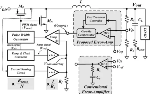
In Fig. 1, a novel error amplifier with on-chip reconfigurable compensator substitutes for the conventional error amplifier to achieve fast-transient response in case of load variations. In other words, the proposed error amplifier not only contains on-chip but also achieves fast-transient response. In Section II, we describe the design of the proposed error amplifier. Exper-imental results are shown in Section III. Finally, we make a conclusion in Section IV.
II. DESIGN OFPROPOSEDCIRCUITS
A. On-Chip Compensated Error Amplifier With Fast-Transient Controller
The schematic of proposed error amplifier is shown in Fig. 2. The current source is composed of transistors
for biasing a cascade operational transconductance amplifier (OTA), which is a single-stage amplifier with a high gain and one dominant pole. The on-chip compensator is composed of 1549-7747/$25.00 © 2007 IEEE
Fig. 1. On-chip compensated error amplifier with fast-transient technique substitutes for the conventional error amplifier in a buck converter.
Fig. 2. Schematic of proposed fast-transient compensated error amplifier.
three transistors , on-chip components and
a voltage follower [7]. According to theorem of cur-rent-mode Miller capacitance, an equivalent current source con-nected to the two terminals of the small capacitor has a current times that of flowing through the small capacitor. In Fig. 2, voltage follower forces the voltage of node to closely track the voltage of node when switch is off and switch is
on. Three transistors , , and , which operate in
linear-region and constitute two parallel on-resistances, have the same large gate–source voltage and small drain–source voltage. One on-resistance is decided by transistor and the other on-resistance is decided by the parallel transistors . The values of these two parallel on-resistances are inversely propor-tional to their respective aspect ratios and shown as
(1)
In order to generate a current that is times larger than the current flowing through a small capacitor , the sum of the
aspect ratio of and is set times that of . Hence,
the equivalent driving current flowing through capacitor is boosted by a factor of . In other words, the equivalent capacitance is multiplied by a factor of and is equivalent to a large off-chip capacitor.
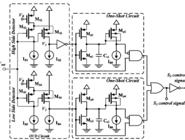
The output capacitor of the error amplifier needs to be charged or discharged as fast as possible for sudden load variations. Thus, when switch is on and switch is off the equivalent current is divided into two parts. One part current is uti-lized to charge or discharge the small capacitor . The other part current is utilized to compensate the dc–dc converters. The detector and fast-transient control circuit in Fig. 3 is used to react to load current suddenly changing from low to high, or vice versa. In order to accurately detect the load variation, the fast-transient control circuit needs two one-shot circuits to get optimum transient response time. The operation of the output voltage detector (OVD) is described as following: and
1152 IEEE TRANSACTIONS ON CIRCUITS AND SYSTEMS—II: EXPRESS BRIEFS, VOL. 54, NO. 12, DECEMBER 2007
Fig. 3. Detective and control circuit for fast-transient response.
are in response to detect the condition that is larger than the desired voltage when load current suddenly changes from heavy to light. and are used to detect the load current from light to heavy. In steady state operation, the current
is larger (smaller) than the due to the
aspect ratio of transistor is larger than that of transistor
. The value of node stay at a high (low) voltage
level if the variation of output voltage is not large enough to trigger OVD circuit to generate one-shot pulse.
Once load current decreases (increases) rapidly and cause to pull high (drop down), then it results in decreasing (increasing) gate–source voltage and increasing (decreasing)
threshold voltage for transistor because of the
modulation voltage between body and source. According to current equation of MOS transistor operating in saturation
region, current drastically shrinks to a smaller
(larger) value than that of current . Consequently,
voltage is pulled down (up) to trigger a one-shot pulse for switching the normal operation mode to the fast-transient
mode. Proper adjustment of bulk-source voltage can
eliminate the possibility of leakage current between source and bulk nodes. When one-shot circuit switches the normal operation mode to the fast-transient mode for a short time, the proposed error amplifier in Fig. 2 has a large current to charge or discharge the small output capacitor ; meanwhile, the transconductance of the proposed error amplifier is increased
from to .
The transconductance in the normal operation mode is shown as the following equation when the tail current of the error amplifier is :
(2) The transconductance in the fast-transient mode is increased
from to , which is shown as
(3)
where is the ratio of to and is the factor of
Miller multiplication. The steeper the slope is, the less the recovery time of the on-chip error amplifier is. The appro-priate values of and are set to 0.5 and 100 for this on-chip compensated error amplifier. Larger value of the product
Fig. 4. Timing analysis of signal waveforms: (a) with a positive and sudden load current variation, and (b) with a negative and sudden load current variation. may make the system unstable and oscillation may occur at the output. Thus, a conservative value is selected for our implemen-tation.
B. Timing Analysis of Fast-Transient Control
An appropriate time [8] can speed up the
tran-sient response and reduce the output voltage ripple significantly. Fig. 4 shows the waveforms of the transient response when load
current has a sudden load current change . Within
the bandwidth smaller than 20% switching frequency, the av-eraged model [9] is used to analyze the characteristics of tran-sient response. For a sudden large load, the insufficient charge
between the current and from time to is
supplied by the output capacitor . The current
in-creases with a slow slope in normal operation. Once
the fast-transient controller is triggered, it increases the slope of
from to . The slopes and
are proportional to the transconductances and of the error amplifier, respectively. The optimum duration
time of is determined when the value of is
slightly larger than that of the load current because the energy is sufficient to supply the load and stops dropping after time . The duty of switching signal is rapidly increased by the fast-transient controller. The new proposed technique can have better performance than that of slew-rate enhancement (SRE) [1] because the output capacitor of the error amplifier is a small capacitor, which needs short charging/discharging time [10].
The fast-transient controller is started to speed up the
in-creasing rate of at time . From time to , the
non-inverting input terminator of comparator in Fig. 1 is expected to rise to a stable voltage, which can be decided by the cur-rent-sensing circuit and V–I converter [11]. When the output is stable, the voltage variation of the noninverting input terminator of comparator is given by
(4) where is current sensing ratio, is the current sensing resistor, , is the resistor for converting current to voltage, and
Once the fast-transient controller triggers a one-shot pulse, the error amplifier only needs to raise the voltage of the inverting input terminator to described as (5). The second term in (5) stands for the voltage drop corresponding to before starting the fast-transient operation. is the magnitude of error amplifier’s transfer function in normal operation mode
(5) The small capacitor is charged by an average current for a period of when the fast-transient controller in-creases the transconductance from to . The increasing charge of the output capacitor and average current are given as
(6) (7)
According to (3), the period of for fast-transient
operation can be derived as
(8) is the case of large negative load as shown in Fig. 4(b) for fast-transient operation. Before time , the output voltage level is slightly lower than the desired voltage because the dc–dc converter is working in the heavy load. Thus, it needs to wait more time than the case of Fig. 4(a) for triggering the fast-transient controller. In other words, is smaller
than .
C. Analytic Pole–Zero Pair of the On-Chip Compensated Error Amplifier
The equivalent resistances of two parallel resistances gener-ated by three transistors working in triode region are modeled as two resistances and . is the equivalent resis-tance of transistors , and is the equivalent resistance of parallel transistors and . A careful effort on symmet-rical layouts of can improve the mismatching problem. Due to the switch frequency of the dc–dc buck converter is designed at 500 kHz, the unity gain frequency is designed below 20% switching frequency. Thus, we model the voltage follower as a transfer function with only one dominant pole at . The transconductance of this voltage follower is . As a result, the transfer function of the voltage follower is shown as (9)
(9)
Furthermore, the output equivalent impedance of voltage fol-lower can be derived as
(10)
where and are the Miller compensation capacitor and
resistor, respectively. is the transconductance of the second stage in the voltage follower. Besides, the output impedance of
TABLE I
SPECIFICATIONS OFBUCKCONVERTER
Fig. 5. Micrograph of the on-chip compensated error amplifier for fast-tran-sient response dc–dc buck converter.
first stage and second stage of this operational amplifier are
and .
The transfer function of on-chip compensator is written as (11) Because the value of is such larger than , the value of low-frequency pole is lower than that of the low-frequency zero by this proposed on-chip compensator and they are described as
and (12)
Obviously, the proposed on-chip current-mode Miller capac-itor can work correctly as a large off-chip capaccapac-itor. The analytic results show the correctness of the equivalent low-frequency pole–zero pair and implementation of the proportional-integral (PI) compensation in dc–dc converters.
III. EXPERIMENTALRESULTS
The fast-transient response dc–dc converter with on-chip compensated error amplifier is implemented with TSMC 0.35- m process. Specifications of the dc–dc converter are listed in Table I. The micrograph of proposed circuit is shown in Fig. 5.
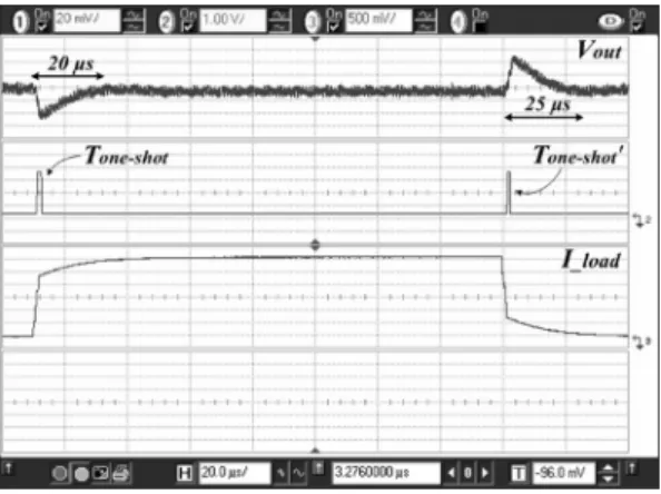
For demonstrating the fast-transient response, the load cur-rent changes from 100 to 400 mA and back to 100 mA with rising time and falling time of 4 s. In Fig. 6, curve (a) illus-trates the conventional error amplifier with external compen-sation resistor and capacitor. This curve needs about 100 s
1154 IEEE TRANSACTIONS ON CIRCUITS AND SYSTEMS—II: EXPRESS BRIEFS, VOL. 54, NO. 12, DECEMBER 2007
Fig. 6. Load transient response with load current step between 100 and 400 mA. (a) Dropout voltage is 160 mV and overshoot voltage is 152 mV by con-ventional error amplifier. (b) Dropout voltage is 160 mV and overshoot voltage is 141 mV by on-chip compensated error amplifier without fast-transient con-troller. (c) Dropout voltage is 40 mV and overshoot voltage is 47 mV by on-chip compensated error amplifier with fast-transient controller.
Fig. 7. Enlarged waveforms of transient response with proposed error ampli-fier.
to stabilize the large load current variation from low to high, or vice versa. Curve (b) is the result of the on-chip compen-sated error amplifier without fast-transient controller. Owing to the same compensated pole–zero pair, the transient response is nearly the same as that of curve (a). Curve (c) shows the result of the on-chip compensated error amplifier with fast-transient mechanism. It has the minimum recovery time and the enlarged waveforms are shown in Fig. 7. The proposed amplifier only needs less than 25 s to recover the output voltage to a stable voltage level when load current changes. The reason why the output voltage level of error amplifier can be recovered rapidly is benefited from an auxiliary current that is times the value of original current.
Moreover, experimental results also prove the correctness of timing analysis of fast-transient control. By (8), and are 2.65 s and 2.23 s, respectively. From Fig. 7,
and are 2.85 and 2.28 s, respectively.
The error percentage for load suddenly changing from low to high and high to low are only 7.23% and 2.54%, respectively. These values slightly deviate from analytic values because of process, temperature and supply voltage variations. Thus, in order to avoid the converter from oscillating, we use conserva-tive value of one-shot timing values to make sure the stability of the system.
IV. CONCLUSION
A novel dc–dc converter with on-chip compensated error am-plifier and fast-transient mechanism is presented in this paper. The error amplifier uses an on-chip reconfigurable Miller capac-itor to improve the transient response at an accurate one-shot time. Experimental results demonstrate the transient speed by our proposed technique is faster than conventional control by about five times, and there is about four times reduction on the dropout voltage compared to that of conventional design. With the proposed error amplifier, the transient response of dc–dc converters is improved significantly.
REFERENCES
[1] H. Lee, P. K. T. Mok, and K. N. Leung, “Design of low-power analog drivers based on slew-rate enhancement circuits for CMOS low-dropout regulators,” IEEE Trans. Circuits Syst. II, Exp. Briefs, vol. 52, no. 9, pp. 563–567, Sep. 2005.
[2] J. Roh, “High-performance error amplifier for fast-transient dc–dc con-verters,” IEEE Trans. Circuits Syst. II, Exp. Briefs, vol. 52, no. 9, pp. 591–595, Sep. 2005.
[3] Z. Hu and D. Ma, “A pseudo-CCM buck converter with freewheel switching control,” in Proc. Int. Symp. Circuits Syst. (ISCAS’05), May 2005, vol. 4, pp. 3083–3086.
[4] K. Yao, K. Lee, M. Xu, and F. C. Lee, “Optimal design of the active droop control method for the transient response,” in Proc. Appl. Power
Electron. Conf. Expo., Feb. 2003, vol. 2, pp. 718–723.
[5] A. Barrado, A. Lázaro, R. Vázquez, V. Salas, and E. Olías, “The fast re-sponse double buck dc–dc converter (FRDB) operation and output filter influence,” IEEE Trans. Power Electron., vol. 20, no. 6, pp. 1261–1270, Nov. 2005.
[6] M. Siu, P. K. T. Mok, K. N. Leung, Y.-H. Lam, and W.-H. Ki, “A voltage-mode PWM buck regulator with end-point prediction,” IEEE
Trans. Circuits Syst. II, Exp. Briefs, vol. 53, no. 4, pp. 294–298, Apr.
2006.
[7] G. Palumbo and S. Pennisi, “A high-performance CMOS voltage fol-lower,” in Proc. IEEE Int. Conf. Electron. Circuits Syst., Sep. 1998, vol. 2, pp. 21–24.
[8] H.-W. Huang, H.-H. Ho, C.-C. Chien, K.-H. Chen, G.-K. Ma, and S.-Y. Kuo, “Fast-transient dc–dc converter with on-chip compensated error amplifier,” in Proc. 32nd Solid-State Circuits Conf., Sep. 2006, pp. 324–327.
[9] R. W. Erickson and D. Maksimovic´, Fundamentals of Power
Elec-tronics. Norwell, MA: Kluwer, 2001.
[10] H.-W. Huang, H.-H. Ho, C.-J. Chang, K.-H. Chen, and S.-Y. Kuo, “On-Chip compensated error amplifier for fast-transient dc–dc converters,” in Proc. IEEE EIT Conf., May 2006, pp. 103–108.
[11] C. F. Lee and P. K. T. Mok, “A monolithic current-mode CMOS dc–dc converter with on-chip current-sensing technique,” IEEE J. Solid-State