A 650 GHz Photonic transmitter Design
Using CPW-fed Slot Antenna
Yi-Chun Yu", Shih-Yuan Chen', An-Shyi Liu', Ruey-Beei Wu' and Chi-Kuang Sun2
IGraduate Institute of Communication Engineering, National Taiwan University, Taipei, Taiwan, 10617, ROC
Email:ruwu~ew.ee.ntu.cdu.hv
'Graduate Institute of Elecho-Optical Engineering, National Taiwan University, Taipei, Taiwan, 10617, ROC
Abstract-In this paper, one planar slot antenna with GaAs substrate for a 6SOGHz edge-coupled photonic transmitter application is demonstrated. In our design, the photonic transmitter consists of the CPW-fed slot antenna, handpstop filter and DC pad. The millimeter wave components a r e cascaded with a metal-semiconductor-metal traveling-wave photodetectors (MSM-TWPD) (11. This design has been fabricated on GaAs substrate and the radiation power is measured by liquid-helium-cooled bolometer. The measurement result shows the feasibility of a compact THz photonic transmitter design excited by a low power laser with a high conversion efficiency.
I. INTRODUCTION
Terahertz technology has drawn more and more attention in recent years. However, the difficulty of generation of THz electromagnetic wave efficiently is a main problem. In general, purely electronic oscillators degrade their performance as the frequency exceeds 100GHz. On the optical side, quantum cascade lasers also show notably roll-off of their emission characteristics below the frequency of 10Thz. Therefore, the emission power exhibits a spectral "black hole" (100GHz-10Thz) in the far infrared spectrum.
Some vertical-illuminated Photonic transmihers have demonstrated the generation of narrow-hand THz waves range from IOOGHz to ITHz. The output power of lOmW at IOOGHz and 120
U
W at 300GHz had been investigated in literatures [2]-[3]. However, the performance of photonic transmitter at higher frequency is not satisfactory. The vertical-illuminated structure and the photonic transmitter with poor light-THz conversion efficiency also make it difficult to be integrated with a low powcr laser.In order to improve the drawbacks shown in the above paragraph, an edge-coupled membrane photonic transmitter with high efficiency is proposed in this paper. The measurement shows the maximum conversion efficiency at 645GHz is about 0.1 I%, corresponding to a maximum average power of 3 . 9 ~ W, and a maximum peak power of 13.2mW under excitation by quasi-CW optical pulse sources.
'This rNdy way Supported in p M by the Ministry of Education, Republic of China, under Grant 89-E-FAO6-24, and the National Science Council under Grant NSC 92-22 IY-E-002-004
11. DESIGN Of ANTENNA
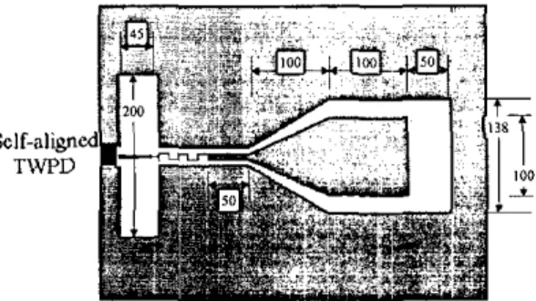
The topology of photonic transmitter in this study is shown in Fig. 1. The photonic transminer is composed of a planar slot antenna, a bandpstop filter, a DC pad, and a metal-semiconductor-metal traveling-wave photodetector (MSM-TPD)[l]. A bias current is fed by a DC probe and the current is conducted by a CPW line. As a result, a DC current is fed through the slot antenna.
To approximately match the impedance of MSM-TWPD, the toial length of slot antenna is designed roughly to be one guided wavelength. The RF signal is converted from the MSM-TWPD. In order to radiate the
RF
signal fully by the slot antenna, one bandstop filter is cascaded with the slot antenna to avoid the RF Dowe1 loss. which leaks to the DC Drobe Dad and decreases the radiation efficiency.The bandoass filter is imDlemented meander line as shown in Fia. I 1. It acts as a high impedance transmission line at the frequency band of the designed slot antenna. And the performance of the meander is the same as a bandstop filter.
The dimensions of the slot antenna are 200 p m and 45pm in length and width respectively. The width of input CPW line is 6 pm and the slot width is 8 p m
.
The width and length of dc probe pad are both 100 pm.
The length of each section in the meander line is 10 pm,
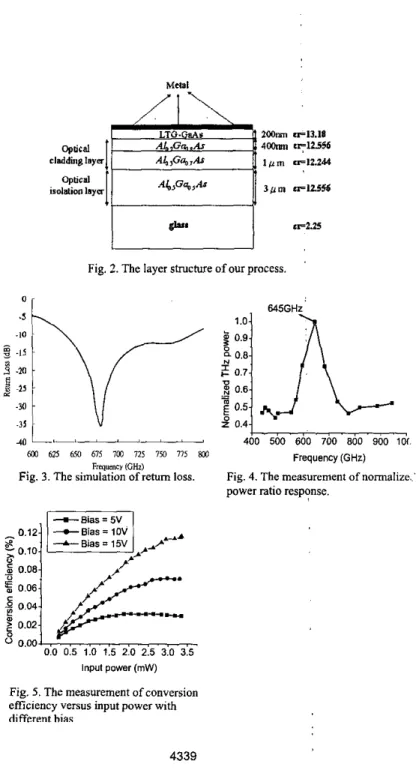
and the width is 2 pm ,The vertical dimensions of our structure are illustrated in Fig.?., which is with gold as the metal layer and the GaAs substrate. And the AlGaAs ( ~ , = 1 3 . 1 8 ) layer below the GaAs substrate acts as a cladding ,layer. The decreasing ratio of AI to Ga in AlGaAs layer and the increasing thickness
of
it are tuned for optimum wave-guiding. In some recent research, a silicon lens is often included to confine the radiation power [4]. But in our edge-coupled design, a large silicon lens will make it difficult to focus laser power on our transminer. To solve this problem, we forsake the large silicon lens, and fabricate our membraneous structure on glass. The glass layer is 150 p m in thickness.111. SIMULATION and MEASUREMEW
The return loss of the designed slot antenna is simulated by full-rjave solver AnSofl Ensemble 6.0 as shown in Fig. 3. As indicated in this figure; the lOdB bandwidth is 22.5% and the center frequency is 680GHz. The conventional vector network analysor can not measure such a high frequency band. Therefore, the radiation power is reflected by a paraboloidal minor, and measured by the Bolometer. The photocurrent measured by the Bolometer is then calculated to the power conversion. The normalized power response versus frequency is shown in Fig.4. In the measurement, the maximum power conversion is at 645GHz. The frequency shift is caused by the large probe pad. Fig. 5. illustrates the conversion eficiency versus input power in different bias voltage. As
shown in this figure, the convcrsion efficiency is directly related with bias voltage. In addition, the photonic transmitter comes to saturation with high input power, and the input powcr of maximum conversion efficiency is increasing with bias voltage. The best convcrsion efficicncy 0.11% occurs at the input power of 3.35 mW as the bias voltage is 15 volts.
IV. CONCLUSIONS
In summary, an edge-coupled membrane terahenz photonic transmitter with dc bias applied on trace line is fabricated. The high conversion efficiency (0.11% corresponding to 3 . 9 , ~ W at 645GHz, while bias voltage is 15V, input power is 3.35mW) is about 20 times higher than the optimum value that has been reported in literature [5] at a similar radiation frequency. By the means of the increasing of bias voltage, the bctter performancc is expected.
V. REFERENCES
[ I ] Ming-Chun Tien, “Edge-coupled Membrane Temhertz Photonic
Transmitters with High Conversion Eficiency”, Master degree thesis,
National Taiwan University. Institute of Electro-optic Engineering.
[2] H. Ito,
T.
Furata, S. Kadama, and T. Ishibashi, “InPilnGaAs uni-travelling-carrier phatodiodc with 310GHz bandwidth,” IEEE Electronics letters vol. 36, pp.1809-1810, 2000.[3] H. Ito, T. Furuta, Y. Hirota, T. Ishibashi, A. Hirata, T. Nagatsuma, H. Matsuo,
T.
Noguchi, and M. Ishiguro, “Photonic millimeter-wave emission at 300GHz using and antenna-integrated uni-travelng-carrier photodiode,”IEEE Electronics letters vol. 38, pp.989-990,2002,
[4] A. Hirata, H. Ishii, and Tadao Nagasuma, “Design and Characterization of a 120-GHz millimeter-Wave Antenna for Photonic transmitters,” IEEE
T r a m On Microwave Theo? andTech “01.49, N0.11, p.2157-2162.
[ 5 ] S. M. duffy, S. Verghese, K. A. McIntosh, A. Jackson, A. C. Gossard, and s. Matsuura, “Accurate modeling of dual dipole and slot dements used with phatamixers for coherent terahertz output power,” IEEE Trans. Microwave Theory Tech. Vol. 49, pp.1032-1038,2001.
Sclf-aligne T\WD
Fig. 1. The topology ofour photomic transmitter. (unit in p m )
Fig. ?. The layer structure of our process fj 0.6 -31
B
0.4 400 500 600 700 800 900 lo(. Frequency (GHz) MO 625 650 675 7m 725 710 775 803 Fnquenc~ ICHOFig. 3. The simulation of return loss. Fig. 4. The measurement of normalize..’ power ratio response.
0.0 0.5 1.0 1.5 2.0 2.5 3.0 3.5
Input power (mW)
Fig. 5. The measurement of conversion efficiency versus input power with different hias