國 立 交 通 大 學
顯示科技研究所
碩 士 論 文
高分子介電材料在噴墨噴印技術之表面形態
研究以及在有機薄膜電晶體之應用
Study on Topography of Inkjet Printed Polymer
Dielectrics and Applications for Organic Thin-Film
Transistors
研 究 生:張明農
高分子介電材料在噴墨噴印技術之表面形態
研究以及在有機薄膜電晶體之應用
Study on Topography of Inkjet Printed Polymer
Dielectrics and Applications for Organic Thin-Film
Transistors
研 究 生:張明農
Student:Ming-Nung Chang
指導教授:謝漢萍
Advisor:Dr.Han-Ping D. Shieh
國立交通大學 電機學院
顯示研究所
碩士論文
A Thesis
Submitted to Display Institute
College of Electrical and Computer Engineering
National Chiao-Tung University
in Partial Fulfillment of the Requirements
for the Degree of Master
In
Display Institute
June 2008
Hsin-Chu, Taiwan, Republic of China.
高分子介電材料在噴墨噴印技術之表面形態研究
以及在有機薄膜電晶體之應用
研究生:張明農 指導教授:謝漢萍 教授
國立交通大學顯示科技研究所
摘要
液珠成膜後的表面形態是噴墨列印技術中一項非常重要的關鍵。對高分
子介電材料來說,本篇論文提出了由溶解度參數所主導的咖啡環效應抑制
模 型 , 來 控 制 其 噴 印 後 液 珠 的 形 態 。 其 中 溶 解 度 參 數 可 以 由 物 質 的
Hildebrand參數來估算。另外為了改善噴塗線以及膜的表面型態,本論文
提出了液珠間距優化的方法,以避免間距過大產生導致液珠不連續或是間
距過小導致膨脹效應。而利用上述方法所噴塗的元件,其載子遷移率可以
達到0.12cm
2/Vs,這些結果顯示我們的方法可以有效的應用在噴墨製程的電
晶體上面。
Study on Topography of Inkjet Printed Polymer Dielectrics
and Applications for Organic Thin-Film Transistors
Student: Ming-Nung Chang Advisor: Prof. Han-Ping D. Shieh
Display Institute
National Chiao Tung University
Abstract
• When an inkjet printed deposit is formed, the topography of the droplet on the
substrate is of great importance. In order to achieve the droplet geometric controllable process
for polymeric dielectrics, a solubility dominated model for suppressing the coffee ring effect
was proposed and demonstrated. The solubility can be evaluated by Hildebrand solubility
parameter. Line and film with improved morphological control were achieved using the drop
spacing optimized method. Printed line and film using this approach can avoid individual
droplets and bulge effect. For the electrical performance of printed device, the mobility is of
as high as 0.12cm2/Vs. These results demonstrate that our methods are potential to be utilized
Table of Contents
Chapter 1 ... 1
1.1 Background of Inkjet printing technology ... 1
1.2 Applications of inkjet printing technology ... 2
1.2.1 Polymer Light-Emitting Diodes (PLED) Displays and Color Filters ... 2
1.2.2 Organic electronic components and circuits ... 3
1.3 Motivation and Objective of this thesis ... 3
1.4 Organization of this thesis ... 4
Chapter 2 ... 6
2.1 Inkjet printing system ... 6
2.1.1 Dorp-on-demand mode inkjet printing ... 7
2.1.2 Precision of inkjet printer ... 8
2.2 Ejection Process ... 9
2.3 Droplet Spreading on a substrate ... 11
2.3.1 Droplet landing ... 11
2.3.2 Spontaneous inertial spreading of droplets ... 12
2.3.3 Wet spreading and the final profile of a droplet ... 12
2.4 Droplet profile after drying ... 14
2.4.1 Coffee ring effect ... 14
2.4.2 The Marangoni effect ... 16
2.5 Line deposition ... 17
2.6 Pattern design, Resolution, and printed Dimensions ... 18
3.2 Materials and Instruments ... 24
3.2.1 Materials ... 25
3.2.2 Instruments ... 26
3.3 Experimental Steps ... 26
3.3.1 Maintenance for printing system ... 26
3.3.2 Droplet analysis ... 28
3.3.3 Fabrication of printed OTFT devices ... 29
3.4 Device Measurement and Analysis ... 32
3.5 Summary ... 33
Chapter 4 ... 34
4.1 Ink selection ... 34 4.1.1 Solute selection ... 34 4.1.2 Solvent selection ... 35 4.2 Surface profile ... 38 4.3 Solubility ... 41 4.4 Line formation ... 444.5 Film formation and printed OTFT ... 49
4.5.1 Film morphology analysis ... 49
4.5.2 Pentacene crystallization analysis ... 50
4.5.3 Electrical Parameters Analysis ... 52
4.5.4 Device Discussions ... 53
4.6 Summary ... 53
Chapter 5 ... 55
5.1 Conclusions ... 55
Figure Captions
Fig. 1-1 The roll-to-roll manufacturing technology for RFID tags fabrication. ... 1
Fig. 1-2 A multicolor OLED display. ... 2
Fig. 1-3 Scheme of inkjet printed all-polymer TFT. ... 3
Fig. 1-4 A mixed-solvent system can induce an inward or outward flow in the droplet. Arrows indicate the direction of circuit. ... 4
Fig. 2-1 Inkjet printers: (a) continuous mode and (b) drop-on-demand mode. ... 6
Fig. 2-2 (a) A typical bubble jet dispenser and (b) a typical piezoelectric jet dispenser. ... 7
Fig. 2-3 Schematic representation of droplet ejection for inkjet printing. ... 9
Fig. 2-4 Processes of film formation in inkjet deposition. ... 10
Fig. 2-5 Three typical applications of inkjet technology: (a) patterned deposition for PLED displays, (b) continuous film deposition, and (c) direct printing of wiring. ... 10
Fig. 2-6 The Behavior of a developing droplet during impact on a substrate. ... 12
Fig. 2-7 Relation between contact angle, the final diameter, and the height of droplets10. ... 14
Fig. 2-8 Deegan’s model for coffee ring effect9. ... 15
Fig. 2-9 Evaporation flux distribution for various contact angles. ... 16
Fig. 2-10 Examples of principal printed line features: (a) individual droplets, (b) scalloped, (c) uniform, (d) bulging, and (e) stacked coins. Drop spacing decreases from left to right. ... 17
Fig. 2-11 Typical line printing features at a moderate temperature. ... 18
Fig. 2-12 Schematic diagram of the designed pixels printed dots: (a) a design with a resolution of 2 x 2 pixels and (b) a design with a resolution of 4 x 4 pixels. ... 19
Fig. 2-13 Schematic view of (a) coplanar and (b) staggered OTFTs. ... 20
Fig. 2-14 Schematic of organic field-effect transistors operation in accumulation mode: (a) VD=VS=VG=0 V, (b) VD=VS= 0 V, VG <0, (c) VS = VD = 0 V, VG >0, (d) VS= 0 V, VG<VD<0, and (e) VS= 0 V, VD<VG<0... 22
Fig. 3-1 Flow chart of the inkjet printing process from droplet analysis to the OTFT devices fabrication. ... 24
Fig. 3-2 (a) The printing instrument Litrex 70L and (b) the key components of the printing
system. ... 27
Fig. 3-3 The droplet checking system for nozzles. ... 27
Fig. 3-4 Array of polymer dots printing at a mutual distance of 101.6μm. ... 29
Fig. 3-5 Scheme of patterned ITO glass, the bars denote ITO electrodes. ... 30
Fig. 3-6 (a) A thermal evaporation system and (b) the over view of the thermal evaporated facility. ... 31
Fig. 3-7 Flow chart of OTFTs fabrication process. ... 31
Fig. 3-8 The flow chart of the fabrication process of the OTFT device. ... 31
Fig. 4-1 Chemical structures of polymeric gate dielectric materials. ... 35
Fig. 4-2 Evaporation flux distribution for various solvents with different vapor pressure. ... 36
Fig. 4-3 Surface profile of the PMMA dots (a) without co-solvent, (b) with THP, (c) with acetophenone, and (d) n-tetradecane as the co-solvent. ... 38
Fig. 4-4 Surface profile of the PαMS dots (a) without co-solvent, (b) with THP, (c) with Acetophenone, and (d) n-tetradecane as the co-solvent. ... 40
Fig. 4-5 Surface profile of the PRFMA dots (a) without co-solvent, (b) with THP, (c) with Acetophenone, and (d) n-tetradecane as the co-solvent. ... 41
Fig. 4-6 A schematic representation of the mechanism of the kinetically develop with (a) high solubility and (b) low solubility. ... 44
Fig. 4-7 Geometry for (a) uniform bead and (b) landed droplet... 45
Fig. 4-8 Geometry of the impinging droplet contact lines. ... 46
Fig. 4-9 The estimation of the radius for an uniform line (Rline) and the radius of a new droplet at impingement (Riminging). ... 47
Fig. 4-10 Cross section of printed lines with different drop spacing: (a) 400DPI (y =1.40), (b) 450DPI (y=1.24), (c) 500DPI (y=1.12), (d) 550DPI (y=1.01), and (e) 700DPI (y=0.80) ... 48
Fig. 4-11 Surface roughness of polymeric gate insulator films: (a) spin-coated and (b) printed film. ... 50
Fig. 4-13 ID-VG curves of printed devices. ... 52
Fig. 4-14 ID-VD curves of printed devices. ... 52
Table of Contents
Table 4-1 Solvent properties at room temperature ... 36
Table 4-2 Ink properties of PMMA, PαMS , and PTFMA in different solvent system. ... 37 α Table 4-3 Coffee ring factor of PMMA in different solvent system. ... 39
Table 4-4 Coffee ring factor of PαMS in different solvent system... 40
Table 4-5 Coffee ring factor of PTFMA in different solvent system... 41
Table 4-6 Hildebrand Solubility parameter of all the materials. ... 42
Table 4-7 Solubility evaluation for PMMA, PαMS, and PTFMA in our solvent system. ... 43
Chapter 1
Introduction
1.1 Background of Inkjet printing technology
In the electronic industries, traditional techniques to deposit inorganic semiconductor materials involve photolithographic etching and controlled vapor deposition. These methods are justified by the market demanding higher operating speeds and the performance of Silicon IC-driven products. However, they are not always the most suitable methods for applications
such as large-area electronics, where further miniaturization is not required1.
To develop such large-area and low-cost fabrication processes in electronics, there is currently a strong interest in inkjet printing technology because it is an additive method in which patterns are fabricated through the selective deposition of materials in specified regions. Such an additive pattern is completed in a single step and remarkably reduces processing time
and material consumption2. Furthermore, there is also an inherent advantage to high
throughput associated with inkjet printing because these manufacturing methods can be utilized to fabricate electric devices directly on a continuous and flexible substrate in
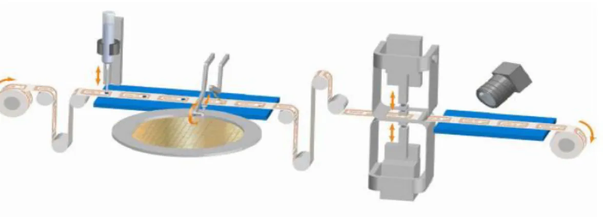
roll-to-roll (R2R) processing 3, as shown in Fig. 1-1.
1.2 Applications of inkjet printing technology
Electronic products using inkjet printing technology can greatly reduce cost than conventional silicon-based electronics. Although the performance for the printed electronics may be lower, there are still a wide variety of applications where low-cost printed electronics could be used. Some of obvious applications include displays, radio frequency identification (RFID) tags, smart cards, electronic sensors, packaging, and printed circuit boards (PCB), etc.
1.2.1 Po
lymer Light-Emitting Diodes (PLED) Displays and Color Filters
Conventionally, solution-processed monochromatic displays can be prepared by
spin-coating, but the fabrication of multicolor displays requires a micro-patterning technique to locally deposit three printing color electroluminescent polymers. At the moment, the most promising approach seems to be inkjet printing. An example of such a display based on inkjet printing technology is shown in Fig. 1-2.
Another display-related field is the fabrication of color filters for liquid-crystal displays (LCDs). Every pixel is printed with inks containing differently colored dyes or pigments to create a multicolor displays. Demonstration of the principle of printed color filters was
reported.5
1.2.2 Organic electronic components and circuits
Advances in the field of conducting polymers can open the way for all-printed electronic components and circuits. Conducting polymers such as poly(3,4-ethylenedioxythiophene) doped with poly(styrene)-sulfonate (PEDOT/PSS), have been proposed to form contacts for polymer thin-film transistors (TFTs), and all-polymer TFTs were also demonstrated by using the inkjet printing process. A schematic architecture of the transistor is shown in Fig. 1-3.
Fig. 1-3 Scheme of inkjet printed all-polymer TFT.
1.3 Motivation and Objective of this thesis
The behavior of droplets on a substrate, and the subsequent line and films that are formed by overlapping droplets is a critical consideration in inkjet printing since the thin-film morphology strongly influences the usefulness of the end product. However, it is commonly observed that after a micro-scaled droplet of the inks is dried, a thin-film with ring-like topography is always formed on the substrates. This effect results in an undesirably uneven distribution of materials across the deposit, which will degrade the performance of the devices.
A significant step toward achieving printed electronics is to thermally control the shape of the droplet while drying.
One approach to improving the homogeneity of printed deposits involves printing from a mixed-solvent system. This approach makes use of the evaporation induced flow and in particular the convective and Marangoni flows that occur in a droplet during drying. The convective flow that transports the solute to the contact line can be counterbalanced or enhanced, depending on the solvent composition as shown in Fig 1-4. Based on this strategy, the evaporation-induced flow in droplets can be controlled by varying the composition the solvent mixture.
In this research, the coffee ring effect was controlled and reversed to improve the uniformity of the deposit. After that, the theories that lead to uniform printed line and film were studied and developed for optimizing their morphologies. Furthermore, the dielectric layer of OTFT was fabricated by using inkjet printing to examine the morphology of the printed film.
Fig. 1-4 A mixed-solvent system can induce an inward or outward flow in the droplet. Arrows indicate the direction of circuit.
1.4 Organization of this thesis
This thesis is organized as follow: The basic knowledge of inkjet printing and the operational principle of OTFTs are described in Chapter 2. The experimental details are
illustrated. In Chapter 4, the mechanism for suppressing the coffee-ring effect in micro-scaled droplets is investigated. The performance of OTFT devices by inkjet printing is also demonstrated and summarized. Finally, the conclusions and future works will be given in
Chapter 2
Principles and Theories
We will introduce the principle of inkjet printing system. Besides, the physical phenomena associated with the topography of thin-film formed by inkjet printing will be reviewed. Finally the operational principle for OTFTs will be described.
2.1 Inkjet printing system
Inkjet printers may operate either in continuous or drop-on-demand (DOD) mode6. In
continuous mode (Fig. 2-1 a), the ink is pumped through a nozzle to form a liquid jet.
Uniformly space and sized droplets are obtained by imposing a perturbation, leading to a surface-tension driven jet ink break-up. Generally, continuous-mode is mainly used for
high-speed graphical applications such as textile printing and labeling. In DOD mode (Fig.
2-1 b), an acoustic pulse ejects ink droplets to form a reservoir through a nozzle. In comparison, the DOD mode is more suitable for electronic industries based on its smaller droplet size and higher placement accuracy.
(a) (b)
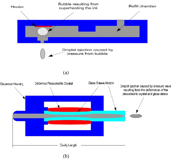
2.1.1 Drop-on-demand mode inkjet printing
In the DOD mode, the acoustic pulse can be generated either thermally or piezoelectrically. In a thermal DOD ejection, solvent is heated to vaporize and a rapidly expanding vapor bubble is created so that an ink droplet is ejected, as shown in Fig. 2-2 (a). The main problem of thermal DOD is that ink always has a lot of restrictions because the ink for industrial application is always temperature sensitive. On the other hand, in piezoelectric DOD mode, ink is expelled by the deformation of a piezoelectric crystal when an electric potential is applied, as shown in Fig. 2-2(b). Piezoelectric DOD is more suitable for a verity of inks because ink degradation is no longer a concern since the pressure wave is generated strictly through mechanical deformation.
(a)
(b)
There are numerous companies producing inkjet printers for industrial printing purposes. Because of using a single nozzle is not realistic in industrial applications, multi-nozzle inkjet printing heads have been invented. The Autodrop Platform from Microdrop was built around eight glass nozzles running in parallel. The 80L and 140P Piezo Micro Deposition System which are develop by Litrex, equip with several hundred of individual nozzles for manufacturing PLED displays.
2.1.2 Precision of inkjet printer
A challenge for inkjet printing system is the precision. The position of a printed drop is affected by several parameters during ejecting process. For instance, an analysis of printed
conductive polymers showed that droplet position can vary by approximately ±11μ m.In the
case of digital lithography, the ejected droplet is positioned along the printing direction by translation of the print head, defined as the x direction. The relative position of a droplet with respect to the position of the print head when the ejection signal is applied is given by the equation: tan cos ut s v us x 2-1
where u is the print head translation velocity, u is the drop ejection velocity, s is the distance between the drop and the print head, θ is the angle of the drop from the normal direction, and t
Fig. 2-3 Schematic representation of droplet ejection for inkjet printing.
The error in printing for the x direction can be approximated by taking the differential of Eq. 2-1 and is given as following:
( ) sec cos v s v s s u u v us x 2-2
Similarly, the error in the y coordinate which orthogonal to the print direction is mainly determined by the angular deviation of the drop and can be represented by the equation 2-3:
2 sec s y 2-3
In general, the translation velocity is 0.1 m/ s, the drop frequency is 10 to 20 kHz, the drop velocity is 6 to 8 m/ s, the distance between the print heads to the substrate is 1 to 5 mm, and the angular drop placement deviation is 0.005 rad. Using these parameters, the expected error in the ejected drop placement is 5-10 μm which correlates well to measure printed droplets from a multi-ejector print head.
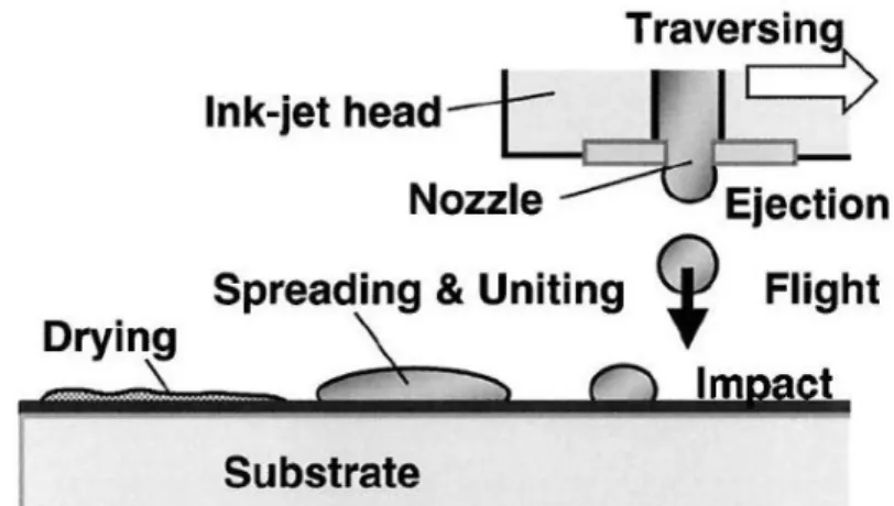
2.2 Ejection Process
from the inkjet nozzle, (2) flight, (3) impact, (4) spreading, and (5) drying. The ejection
process can be used to pattern a thin-film or a directly wiring as shown in Fig. 2-5. The
deposition process of pattern for an organic electro luminescence (EL) display is shown in
Fig. 2-5 (a). The display consists of many pixels, and the three primary colors (red, green, and blue) are printed on the substrate. It is important to control the spreading of the droplets between the bank and the surface surrounding the bank. The deposition process of continuous films for large scale integration circuit (LSI) or liquid crystal displays (LCDs)
manufacturing is illustrated in Fig. 2-5 (b). Several types of thin films can be patterned by
inkjet printing such as photoresist and dielectric layers. The droplets are ejected onto the
substrate and formed a thin film. The direct printing of wiring is shown in Fig. 2-5 (c).
Conductive ink is printed to form a circuit without masking.
Fig. 2-4 Processes of film formation in inkjet deposition.
(a) (b) (c) Fig. 2-5 Three typical applications of inkjet technology: (a) patterned deposition for PLED
2.3 Droplet Spreading on a substrate
2.3.1 Droplet landing
A droplet striking a solid surface exhibits complicated behaviors as shown in Fig. 2-6. A
Droplet spreading onto the substrate consists of an initial spontaneous spreading for a short time and then a wet spreading for a longer time. A droplet that hits a solid surface expands in
the radial direction and reaches a maximum diameter D cmax. If the surface energy is excess at
this time, the droplet diameter decreases as liquid flows toward the center of the droplet. This is called recoiling. Then the droplet might rebound when the energy is excess. If there is still much energy, the droplet vibrates, repeatedly increasing and decreasing it diameter. The time between these expansions and contractions is several microseconds, and the droplet settles into a nearly stable shape when the energy is dissipated.
The droplet shape then slowly changes to the final profile with the minimum surface energy. This is called as “wet spreading.” The contact angle if the droplet becomes a static one
and the droplet diameter asymptotically approaches the final equilibrium diameter (Df) the
time between the beginning of wet spreading and the attainment of the Df ranges from several
Fig. 2-6 The Behavior of a developing droplet during impact on a substrate.
2.3.2 Spontaneous inertial spreading of droplets
The spontaneous spreading of a liquid droplet has been investigated in various field of engineering. Asai model is a semi-empirical formula intended for the droplets with the size of
those produced by an inkjet printer7. The relation between the maximum diameter (Dcmax) and
viscosity (μ) was examined by using the equation:
] Re 48 . 1 exp[ 48 . 0 1 0.5 0.22 0.21 0 max We We d Dc 2-4
where We and Re are the Weber number Reynolds number, respectively.
2.3.3 Wet spreading and the final profile of a droplet
Because Reynolds number, Weber number, and contact angle for droplet-spreading are small, the recoiling is thought to be not observed. After spreading is the maximum diameter
1 3 1 0 1 3 0 1 3 1 ) ( ) 3 ( m m m m x t C V t t D 2-5
where Cx is an experimental constant, m is a physical properties, and t0 is an initial time. The
physical constant m, ideally 3, is depended on material properties. It is assumed here to connect the spontaneous spreading and wet spreading that droplets reach their maximum
diameter at t =0 and that this diameter is the value given by Eq. 2-5. When Cx = 1, the relation
between t0 and Dcmax can be expressed as following:
m m c V D t 0 1 3 max 0 3 2-6
Ideally, a spherical cap is the final profile of the droplet because it has the minimum surface energy. However, various shapes that are different from spherical cap are actually seen, presumably because the contact angle differs from place to place according to the condition if
the material, dirt, and roughness. The final diameter (Df) and final height (Hf) at the center of
the ideally final shape are written as the function of the contact angle (θc) on the substrate and
droplet diameter before impacting (d0):
3 1 4 2 0 ) 2 ( sin ) 2 ( sin 2 3 1 sin c c c f d D 2-7 3 1 4 2 2 0 ) 2 ( sin ) 2 ( sin 2 3 1 sin c c c f d H 2-8
This final droplet shape is determined by the droplet volume and the contact angle, but uncorrelated with the physical properties of liquid. The relations between the final diameter,
Fig. 2-7 Relation between contact angle, the final diameter, and the height of droplets10.
2.4 Droplet profile after drying
Even though the liquid surface is flat, the surface of the dried film can not be confirmed to be flat. When a spilled droplet of coffee dries on a solid table, it leaves a dense, ring-like deposit along the perimeter. Such ring deposits are common wherever droplets containing dispersed solid evaporate in a surface. The ring-like phenomenon can be explained by
evaporation-rate distribution theory, which was proposed by Deengan et al10.
2.4.1 Coffee ring effect
In the theory, an outward flow in a drying droplet of liquid is produced when the contact line is pinned so that liquid is removed by evaporation form the edge of the droplet must be
replenished by a flow of liquid form the interior as shown in Fig. 2-8. This flow is capable of
transferring 100% of the solute to the contact line and thus accounts for the high perimeter concentration of many strains. The evaporation flux has a universal form that depends only on the shape of the droplet. In the evaporation process, liquid molecules interchange rapidly
Fig. 2-8 Deegan’s model for coffee ring effect10.
The vapor quickly approaches the steady-state diffusion equation,
0 ) (
2
r 2-9 where Φ(r) is a steady-state concentration profile. The derivative at the surface gives the evaporating flux, ) ( ) (r D r J 2-10
where D is the diffusion coefficient of the vapor in air. For the droplet with the contact angle
θc on the substrate, the evaporation flux can be expressed by Eq. 2-11,
( ) ) (r R r J f 2-11
where ( 2c) (22c) and Rf Df 2 . As the contact angle decreases and
towards zero, λ approaches to 1/2. We noticed by this theory that the evaporating flux J
becomes uniform when the contact angle is /2 because λ becomes zero. The
evaporation-flux distribution in the radial direction is shown in Fig. 2-9 for various contact
Fig. 2-9 Evaporation flux distribution for various contact angles11.
When the contact angle of droplets at the edge is of less than 90o, the evaporation rate
becomes high. A large amount of solutes might then accumulate at the edge as flow from the central area replaces the evaporating liquid.
2.4.2 The Marangoni effect
The Marangoni flow is generated form a surface tension gradient12. During evaporation,
evaporative cooling reduces the droplet surface temperature non-uniformly. The temperature at the liquid-air interface on the top center of the droplet is the lowest due to a longer thermal conduction path, and the surface tension is the highest there. This produces an inward flow near the droplet surface, whose shear stress balances the Marangoni stress, i.e., the surface tension gradient.
When using a mixture of a low- and a high-boiling solvent, the composition at the contact line will shift toward a higher fraction of higher-boiling solvent than in the buck, due
to the increased rate of evaporation at the edge13. Therefore, the rate of evaporation at the
2.5 Line deposition
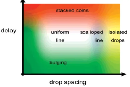
Few principal features emerge when examining printed patterns across a variety of drop space, delay period, and substrate temperature. The feature of printed line can be classified into individual droplets, a scalloped line, a uniform line, a bulging line, and stacked coins as
shown in Fig. 2-10.
If one printed droplets that are too far apart to interact, isolated droplets land and dry
independent of substrate temperature and delay period as shown in Fig. 2-10 (a). At lower
temperature, as droplet spacing decreases, isolated droplets overlap and merge but retain
individual rounded contact lines, and a scalloped pattern emerges as shown in Fig. 2-10 (b).
These scalloped lines are narrower than an isolated droplet as fluid expansion is partially arrested. Further decreasing the droplet spacing will eliminate the scalloping and lead to a
smooth, straight line as shown in Fig. 2-10 (c). These lines have a uniform smooth edge and
top. They are the narrowest lines printed.
Printed droplets even closer together lead to discreet bulging along the line’s length, separated by regions of uniform narrow lines. These bulges tend to form periodically and also
(a) (b) (c) (d) (e)
Fig. 2-10 Examples of principal printed line features: (a) individual droplets, (b) scalloped, (c) uniform, (d) bulging, and (e) stacked coins. Drop spacing decreases from left to right.
at the beginning of the line. Duineveld gives this striking behavior excellent consideration14. Essentially, additional fluid from printing exceeds a bead’s equilibrium contact angle, and discreet regions of outflow result, leading to rounded bulges in the dried feature as shown in
Fig. 2-10 (d). If the substrate temperature increases such that the evaporation time of a single droplet is less than the jetting period, then each landing droplet will dry individually
regardless of overlap, leading to what looks like offset stacked coins as shown in Fig. 2-10 (e).
At a given substrate temperature, increasing the droplet delay period will affect the onset of the stacked coin feature. Droplet spacing has no effect on the width of the lines printed in this regime because each droplet dries individually. Each of these features tends to be found
relative to one another at an intermediate temperature is schematically shown in Fig. 2-11.
Fig. 2-11 Typical line printing features at a moderate temperature15.
2.6 Pattern design, Resolution, and printed Dimensions
A schematic diagram of the design of pixels and printed dots is shown in Fig. 2-12. The
objects are defined as the number of pixels in the x and y directions, which are referred to as the process (printing) direction and normal direction, respectively, in this study. In designing the object, it is possible to generate two images with the same dimensions but different design
printed results with different design resolutions are not the same due to the overlap of dots. The overlap of the dots is determined from the diameter of the droplet, the spreading of the droplet on the substrate, and the printing resolution. The printing resolution is typically expressed as dots per inch (DPI). The center-to-center distance between two dots, hereafter called the dot pitch (DP), is solely dependent on the DPI. If the dot diameter is known, the dimensions of printed results can be calculated by the following equation,
n
DP DW 1 2-12
where W is the width, n is the number of pixels, DP is the dot pitch defined by 25400um/DPI, and D is the diameter of the printed dot.
(a) (b)
Fig. 2-12 Schematic diagram of the designed pixels printed dots: (a) a design with a resolution of 2 x 2 pixels and (b) a design with a resolution of 4 x 4 pixels.
The thickness of the printed lines can be estimated by simple mathematics. Imagining the simple lines with x pixels in the process direction and pixels in the normal direction, the thickness of the printed lines would then be the product of the total volume of the droplets and the volume fraction of the particles in ink divided by the area, which can be expressed by the equation,
v DP y D DP x D y x R Thickness 1 1 2 3 4 3 2-13where R is the radius of the ejected droplet, x is the number of pixels in process direction, y is the number of pixels in normal direction, D is the diameter of printed dot, DP is the dot pitch defined by 25,400 μm/DPI, and v is the volume fraction of the particles in the ink. As the width of the printed lines increases, the ink volume increases faster than the covered area. For example, one can consider a trace with a width of one pixel and a length of 1 cm. If the dot diameter is 100μm and the printing resolution is 500 DPI, there are 196 dots in a 100 x 10,000μm line. If the width of the line is designed to be five pixels, there are 979 dots in a 303 x 10,000μm line. Thus, the number of dots increases fivefold while the printed area increases only threefold. Therefore, the thickness increases with increasing width for a printed trace.
2.7 Operational basics of organic field effect transistors
Generally, organic thin film transistors (OTFTs) are composed of three components: semiconductor, insulator, and electrodes. The configuration of these elements with two different structures, inversed staggered type OTFTs and the inverted coplanar type OTFT are
shown in Fig. 2-13. The electrical characteristics of OTFTs can be adequately described by
models developed for inorganic semiconductors.
The OTFTs could be divided into two families, according to the kind of charges transported by the semiconductor. In semiconductors with n-type channel, the charges transported by them are negative. On the other hand, in semiconductors with p-type channel, the charges transported are positive. Organic semiconductors with p-type channel are the most used for building organic transistors, due to their higher stability under ambient conditions, when compared to the n-type ones.
P-type OTFTs are used here to demonstrate typical I-V characteristics of OTFTs. When the gate electrode is biased positively with respect to the grounded source electrode, they operate in the depletion mode, and the channel region is depleted of carriers resulting in high channel resistance. When the gate electrode is biased negatively, they operate in the accumulation mode and a large concentration of carriers is accumulated in the transistor channel, resulting in low channel resistance. For n-type TFT operation, the electrode polarity is reversed and the majority carriers are electrons instead of holes.
For instance, a p-type semiconductor is shown in Fig. 2-14 (a) When VD=VS=VG =0V, a
negative bias is forced on the gate to form the ohmic current ISD. After that, when VD=VS=0V
and VG<0V, the gate current would across insulator layer and some area of
insulator-semiconductor interface would bend the band gap of the semiconductor. Then, the
accumulation region is formed as shown in Fig. 2-14 (b). The ohmic contact between source
and drain electrodes leads additional charges occur. When positive charges are applied on the gate electrode, an opposite curved band gap would be occurred in the insulator-semiconductor interface. This result conducts the depletion region of carriers. The higher bias on the gate electrode, the larger depletion region expands. Finally, all of the semiconductor layer will be depleted. The voltage across the insulator and semiconductor layer depends on the position of the channel is a functional relationship when drain voltage has strongly negative bias effect
(a) (b) (c)
(d) (e)
Fig. 2-14 Schematic of organic field-effect transistors operation in accumulation mode: (a) VD=VS=VG=0 V, (b) VD=VS= 0 V, VG <0, (c) VS = VD = 0 V, VG >0, (d) VS= 0 V, VG<VD<0,
Chapter 3
Experiment and Instruments
Inkjet printing technology can be used to simplify the fabrication process in electric industries. To develop a reliable printing process, several parameters must be considered to suppress the coffee ring effect. In this chapter, the analysis of dot profile and film formation will be depicted, and the fabrication flow of printed OTFTs will also be described.
3.1 Process Design and Schemes
The inkjet printed thin-films are deposited by overlapping several dots. Therefore, the feature of single droplet will affect the patterns design. For this purpose, steps to deposit uniform thin-films are divided into two parts: droplet analysis for droplet deposition and parameters optimization for thin-film formation. Droplet analysis is accomplished by varying the composition of the solvent mixture. The printed thin-film adopt as the dielectric layer of OTFTs to examine the thin-film quality. The details of the fabrication process are illustrated in Fig 3-1.
Fig. 3-1 Flow chart of the inkjet printing process from droplet analysis to the OTFT devices fabrication.
3.2 Materials and Instruments
In this experiment, a large amount of chemical materials and instruments were used. The arrangement of resources, materials titles, chemical formula and the functions of chemical materials in this section are summarized in Table. 3.1. The fabrication facilities and analyzers are listed in Table 3.2 and Table 3.3, respectively.
3.2.1 Materials
Table 3.1 Experimental materials
Material Abbreviation Company Molecular weight (Mw;g/mol)
Density (g/cm3)
Poly(methylmethacrylate) PMMA Acros 15000 1.14
poly(α-methylstyrene) PαMS Aldrich 20000 1.04
Poly(2,2,2-trifluoroethylmethlyacrylate) PTFMA 30000 1.20
Propylene glycol monomethyl ether acetate
PGMEA Acros 132.2 0.97
1,2,3,4 tetrahydronaphthalene THP Alfa Aesar 132.2 0.97
n-tetradecane Alfa Aesar 170.3 0.78
acetophenone Alfa Aesar 120.2 1.03
Gold Au Goldrex corp 197.0 19.30
pentacene Fluka 278.4 1.00
Table 3.2 Fabrication instruments Instruments Company Function
Ink-jet printing facility Litrex 70L Thin film deposition
Thermal Evaporator ULVAC Active layer and electrodes deposition
3.2.2 Instruments
Table 3.3 Measurement instruments
Instruments Company Purpose
Optical Microscope (OM) Olympus Device scales measurement
Contact Angle detector Paul. N. Gardner Hydrophobic ability observation
Semiconductor Analyzer Keithley 4200 Device performances characterization
Enhanced Phase Scanning Interferometry
SNU SIS1200 Film morphology and
thickness observation (scanner stroke > 30um)
Atomic Force Microscope (AFM)
Veeco DI 3000 Film morphology and
thickness observation (scanner stroke < 30um)
Viscosity meter Brookfield Insulator viscosity measurement
3.3 Experimental Steps
3.3.1 Maintenance for printing system
The solvent maintenance in the printing system includes print head, pipe, and valve systems are an important procedure for the printing facility. Because the printing method has
system. The printing system Litrex 70L and the photograph of the print-head are shown in Fig. 3.2.
(a) (b)
Fig. 3-2 (a) The printing instrument Litrex 70L and (b) the key components of the printing system.
To enhance the performance of print-head, isopropyl alcohol (IPA) was used to develop the droplet calibration and droplet analysis. The droplet checking process was monitored with a built-in program and was shown in Fig. 3.3. After checking, the printing process was ready for proceeding.
Instruction manual
Workable nozzles (green bars represented) Impractical nozzle (red bar represented)
Real time droplet images
3.3.2 Droplet analysis
(1) Preparation of inks
Three different polymeric materials including Poly(methylmethacrylate),
poly(α-methylstyrene), and poly(2,2,2-trifluoroethylmethacrylate) were dissolved in propylene glycol monomethyl ether acetate (PGMEA )with additive solvents, such as 1,2,3,4 tetrahydronaphthalene, n-tetradecane, and acetophenone with 15 wt%. The concentration ratio of primary and additive solvent is 8 to 2. All of the above mentioned solutions were stirred for 20 minutes and degassed with ultrasonic for 30 minutes. After solution preparation, the solution was filtrated through a filter with 40 μm pore diameter.
(2) Substrates cleaning
The glass slides with a dimension of 3cm x 3 cm were cleaned by DI water, acetone, and IPA, and then treated with ultrasonic. Sequentially, the cleaning was carried out by blowing
off the moisture and baking at 100 oC.
(3) Droplet Deposition
The droplets were deposited by using a deposition Litrex 70L inkjet printing system. The voltage waveform was controlled with the pulse voltages of 55 V to 65 V and pulse widths of 5.0 to 7.5 μs to eject the droplets with volume of 30 to 40 picoliters. The vertical distance between the nozzle and the substrate was typically 0.5 mm. A dot array with the dot pitch (DP) of 101.6 μm is shown in Fig 3-4.
Fig. 3-4 Array of polymer dots printing at a mutual distance of 101.6μm.
(4) Fabrication of lines and thin-films
To fabricate lines and thin-films, printing patterns were designed to achieve the droplet overlapping. The substrate temperatures were varied form room temperature to 60
o
C and the dot pitch was varied from 20 to 80 μm. Jetting period from 100 to 500 Hz were appended, through clogging of the nozzles became a problem at a shorter period. After
printing process, the substrate was baked at 100 oC for one hour by hot plate.
3.3.3 Fabrication of printed OTFT devices
An indium tin oxide (ITO) patterned glass substrate was used as the gate electrode for simplicity. The dielectric layer of OTFTs was deposited by inkjet printing technology. The jetting conditions were determined form the droplet analysis. After the deposition of the gate dielectric layer, pentacene, the active layer, was deposited by thermal evaporation. Transistors were developed by thermal evaporation of patterned gold onto defined source/drain contacts. The details of each fabrication process are described in the following section.
(1) Indium tin oxide patterning 1000μm
As shown in Fig. 3-5, glass with well-defined ITO was used as a substrate. After cleaning, the photoresist was spun on, soft baked for 2 minutes, and exposed under UV
exposure for 100 seconds. Photolithography process was carried out by using NaOH(aq).
Etching process was conducted after lithography using a H2SO4 solution. Finally, the
residual photoresist was removed by acetone.
(2) Organic active layer and metal electrodes deposition
The flowchart and the device structure are depicted in Fig. 3-7. The thermal evaporation system shown in Fig. 3-6 was employed to deposit the pentacene and gold electrodes. The
evaporation rate for pentacene was 0.3~0.4 Å /sec at a pressure of 6 x 10⁻⁶ torr and the total
thickness was controlled at 600 Å. Subsequently, the gold electrodes were deposited onto the
active layer with an evaporation rate of 2~3 Å /sec at a pressure of 3 x 10⁻⁶ torr.
(a) (b)
Fig. 3-8 The flow chart of the fabrication process of the OTFT device.
Fig. 3-6 (a) A thermal evaporation system and (b) the over view of the thermal evaporated facility.
3.4 Device Measurement and Analysis
(1) Surface profile
An enhanced phase scanning interferometry (EPSI) was utilized to measure the surface profile of printed depositions. EPSI using Michelson white light optical non-contact interferometry to measure the phase shift between the test wavefront and the reference wavefront, therefore, the surface profile the sample can be determined. This kind of measurement system produces fast, non-contact, and true three-dimensional area measurements for both large steps and rough surfaces to nanometer accuracy.
(2) Film morphology
An atomic force microscope (AFM) was utilized to measure the thin film morphology of printed depositions. The operation of AFM was set to tapping mode, and the probe oscillation frequency was 300 Hz. The adopted tapping mode overcame the limitations arose due to thin layer of the condensed phase that formed on most sample surfaces in an ambient imaging environment. The grain size and shape of pentacene are critical while pentacene crystalline deposited on the different insulator layer. Measurements of the grain morphology by AFM were operated under the atmosphere condition.
(3) Electrical characteristics of OTFT devices
The electrical characteristics of the devices, such as degradation and hysteresis, can be evaluated by Keithley 4200 semiconductor analyzer. In addition, the relationship between
3.5 Summary
The relationship between the surface profile of printed droplets and the composition of the solvent mixture was investigated. After droplet analysis, the parameters such as surface pretreatment, jetting period, drop spacing, and substrate temperature were optimized to develop a reliable printing process. Finally, a printed film was adopted as the dielectric layer in the OTFT. All of the experimental results and discussions will be presented in Chapter 4.
Chapter 4
Result and discussions
4.1 Ink selection
Determining the appropriate combination of solvents and solutes is crucial for achieving
the successful printing of polymers and obtaining homogeneous films. The physical properties
of inks, such as viscosity and surface tension, must be compatible with the nozzles and the
toxicity is also considered for industrial applications. They are always the trade-off between
device performance and practicability.
4.1.1 Solute selection
Commercially available polymeric dielectrics, i.e. PMMA and PαMS, were selected to
achieve the reliable electrical properties. In order to suppress the coffee ring effect, the
evaporation rate near the contact line must be slow down. Therefore, one possibility is to
increase the contact angle of the ink on the substrate. Based on this print of view, a material
with hydrophobic functional group, PTFMA, which was modified from PMMA by synthetic approaches, was also introduced. The chemical structure of those polymeric gate insulators are shown in Fig. 4-1.
O
CH
3
CH
3
O
[
]
n
n
]
[
CH
3
[
]
n
O
O
CH
2
CF
3
CH
3
PMMA PαMS FTFMA
Fig. 4-1 Chemical structures of polymeric gate dielectric materials.
4.1.2 Solvent selection
Since ring formation could not be prevented by using a single solvent with a vapor pressure either high or low, solvent mixtures were selected to investigate for coffee ring effect
suppression. To lower the solvent evaporation rate near the contact line, another option is to
add a solvent with low vapor pressure into the ink as a co-solvent. When the droplet is drying,
the solvent is being transported from the center of the circular to the periphery to maintain the
contact line fixed and replenish evaporation losses. However, as co-solvent evaporates slower
than the primary solvent, the concentration of the co-solvent at the periphery will gradually
increase. The phenomenon will cause a decrease in the local vapor pressure, and a decrease in
the rate of evaporation at the edge and the amount of the solvent mixture that is transported
from the center to the edge.
A low boiling point solvent with low toxicity, PGMEA, was selected as the primary solvent, and three high boiling solvents, Acetophenone, THP, and n-tetradecane, were selected
as the co-solvents. The boiling point and vapor pressure of these solvents were listed in Table 4-1 and the evaporation flux distribution of these solvent is shown in Fig. 4-2. It is observed
that the evaporation flux of the co-solvent near the contact line (r/RD=1) is very close to that
of the primary solvent near the central regime (r/RD=0).
Table 4-1 Solvent properties at room temperature
Solvent Boiling point (oC) Vapor pressure (mmHg) PGMEA 146 10.90 Acetophenone 202 0.45 THP 208 0.18 n-tetradecane 253 1.00
The viscosity and the surface tension of these inks were measured in room temperature and the results are illustrated in Table 4-2. The relationship between the spreading factor
(Dmax/do) to the viscosity and surface tension was calculated using Asai’s model as mention
above6, and the results were also shown in Table 4-2. The spreading factor indicates spreading
trend of the droplet on the substrate. In all case, the differences of spreading factor in different co-solvents were of less than 5.5%. As the result, the spreading behavior would not be affected by our solvent systems.
Table 4-2 Ink properties of PMMA, PααMS , and PTFMA in different solvent system.
Solute Co-solvent Surface tension (mN/m) Viscosity (cp; 25 oC) Dmax/d0 Difference PMMA none 27.7 4.78 1.64 3.80% Acetophenone 28.8 5.2 1.62 THP 27.6 6.06 1.59 n-tetradecane 25.3 6.34 1.58 PαMS α none 23.9 2.61 1.78 5.32% Acetophenone 28.9 3.50 1.69 THP 27.7 3.06 1.72 n-tetradecane 26.7 3.36 1.70 PTFMA none 27.3 3.00 1.74 4.82% Acetophenone 27.7 3.79 1.68 THP 26.4 4.47 1.66 n-tetradecane 25.6 4.05 1.67
4.2 Surface profile
Initial experiments were performed to verify the influence of the solvent mixture with solutions of PMMA in our solvent system. A single dot of PMMA printed form pure PGMEA on glass substrate is shown in Fig. 4-3 (a). A ring like deposition results from the convective flow in the droplet during drying process, as mentioned above. When acetophenone, which has a higher boiling point than PGMEA, is added as a co-solvent at 20% by weight, and a more uniform printed dot can be achieved as shown in Fig. 4-3 (b). This outcome is due to the slow evaporation at the contact line, which results in decreasing convective flow.
(a) (b)
(b) (d)
Fig. 4-3 Surface profile of the PMMA dots (a) without co-solvent, (b) with THP, (c) with acetophenone, and (d) n-tetradecane as the co-solvent.
The ratio of coffee height at central dot is called coffee ring factor is defined to evaluate the coffee ring effect. High coffee ring factor indicates that the droplet deposit is suffered
For PMMA with THP and Acetophenone as the co-solvent, the coffee ring factor is decreased to 3.09 and 3.00, respectively. Therefore, acetophenone has the stronger ability to suppress
the coffee ring effect than THP. However, for PMMA with n-tetradecane as the co-solvent,
the coffee ring factor cannot be measured because the surface profile is very irregular.
Table 4-3 Coffee ring factor of PMMA in different solvent system.
Solute Solvent Co-solvent Coffee ring factor PMMA PGMEA none 6.88
PGMEA THP 3.09
PGMEA Acetophenone 3.00
PGMEA n-tetradecane -
Printing experiments were repeated with PαMS as the solute in our solvent system. A single dot of PMMA printed from pure PGMEA on glass substrate is shown in Fig. 4-4 (a). In this case, the PαMS dot is larger than PMMA dot because the viscosity is much lower. The coffee ring factors are shown in Table 4-4, and THP co-solvent has the stronger ability to suppress the coffee ring effect than acetophenone. Similarly, the surface profile for n-tetradecane is still irregular. Irregular deposition always results from poor solubility of the solvent to the solute. To verify this assumption, the solubility of our solvent to the solute were calculated by solving the Thermodynamics of the system in the next section.
(a) (b)
(b) (d)
Fig. 4-4 Surface profile of the PαMS dots (a) without co-solvent, (b) with THP, (c) with Acetophenone, and (d) n-tetradecane as the co-solvent.
Table 4-4 Coffee ring factor of PαMS in different solvent system.
Solute Solvent Co-solvent Coffee ring factor PαMS PGMEA none 5.00
PGMEA THP 4.00
PGMEA Acetophenone 4.16
PGMEA n-tetradecane -
The coffee ring formation is not obvious for PTFMA case even without the co-solvent, as shown in Fig 4-5. The ring height is always lower than the center height. Therefore, the coffee ring factors are below one as listed in Table 4-5. Similar to the PMMA and PαMS, the
(a) (b)
(b) (d)
Fig. 4-5 Surface profile of the PRFMA dots (a) without co-solvent, (b) with THP, (c) with Acetophenone, and (d) n-tetradecane as the co-solvent.
Table 4-5 Coffee ring factor of PTFMA in different solvent system.
Solute Solvent Co-solvent Coffee ring factor
PTFMA PGMEA none <1
PGMEA THP <1
PGMEA Acetophenone <1
PGMEA n-tetradecane -
4.3 Solubility
The Hildebrand solubility parameter (δ) provides a numerical estimate of the degree of interaction between materials, and can be a good indication of solubility, particularly for non
polar materials such as many polymers16. Materials with similar values of δ are likely to be miscible.
The Hildebrand solubility parameter is the square root of the cohesive energy density:
m v V RT H ) (
where △Hv is the energy of vaporization of species and Vm is the molar volume of species.
Materials with similar solubility parameters will be able to interact with each other, resulting in solvation, miscibility or swelling.
The Hildebrand solubility parameters of PMMA and PαMS are listed in Table 4-6, the
different values of Hildebrand solubility parameter (δs –δp) are listed in Table 4-7, where δs is
the Hildebrand solubility parameters of polymers and δp is that of the solvent. For the different
value (δs –δp) higher than 1.0, it means low solubility (LS); for the different value lower than
1.0, it means high solubility (LS); in between, it means medium solubility (MS).
Table 4-6 Hildebrand Solubility parameter of all the materials.
Hildebrand parameter (cal/cm3)1/2 PGMEA 10.1 THP 9.5 Acetophenone 10.6 n-tetradecane 7.9 PMMA 10.2 PαMS 9.7 PTFMA 6.8
Table 4-7 Solubility evaluation for PMMA, PαMS, and PTFMA in our solvent system. Hildebrand parameter for PMMA (δp-δs;cal/cm3) Hildebrand parameter For PαMS (δp-δs;cal/cm3) Hildebrand parameter For PTFMA (δp-δs;cal/cm3)
PGMEA 0.1(HS) 0.4(HS) 3.3 with H-bond
Acetophenone 0.4(HS) 0.9(MS) 3.8 with H-bond
THP 0.7(MS) 0.2(HS) 2.7 with H-bond
n-tetradecane 2.3(LS) 1.8(LS) 1.1(LS)
HS = High solubility, MS = Medium solubility, and LS = Low solubility
The decreasing order of solubility of PMMA in different co-solvents is Acetophenone > THP > n-tetradecane. And the ability to suppress the coffee ring effect is Acetophenone > THP > n-tetradecane. Therefore, the solubility dominated model for coffee ring suppressing is established as follow.
The drop initially spreads rapidly on the substrate and attains a quasi-equilibrium contact angle. The solute concentration in the drop increases with time due to evaporation of solvent. Furthermore, the composition of the droplet at the contact line will shift toward a higher fraction of low vapor pressure solvent, the co-solvent, than in the bulk, due to the increased
rate of the evaporation at the edge. According to the kinetic crushing model17, the slower
evaporation at the contact line where there is a higher concentration of solvent with good solubility allows the molecules to diffuse away from the contact edge before the concentration reaches the critical concentration. Therefore, a homogeneous deposition can be achieved. For the opposite case, when the co-solvent has poor solubility, the molecules will precipitate
rapidly and result in an irregular deposition. The mechanism for the formation for homogeneous or irregular deposition is shown in Fig 4-6.
(a)
(b)
Fig. 4-6 A schematic representation of the mechanism of the kinetically develop with (a) high solubility and (b) low solubility.
4.4 Line formation
Before thin-film fabrication, understanding line formation is a key issue. Typically, the line height will increase when the drop spacing is decreased. However, the printed line will become unstable when the contact angle of the liquid with the substrate is larger than the advancing contact angle. A small disturbance can grow into bulge as shown in Fig 2-10 (d).
To evaluate the minimum drop spacing, the volume of fluid being deposited per unit length is considered: Δx V h unit_lengt volume drop 4-1
x V f R drop 2 1 2 1 4-2where f(θ) is the contact angle factor to correct the cross-sectional area of the half-cylinder bead appropriately from its ideal circular cross section. The relevant geometry is shown in Fig. 4-7 (a).
The correction factor f (θ) can be determined from the height equation for a wetting drop of
radius R1 with a finite contact angle and be solved by calculate the actual cross-section area of
the cylinder:
tan sin 1 2 2 2 1 R r R r h 4-3 ) ( 2 1 ) ( 12 sec _ 1 1 R f r drh A R R tion cross
4-4 cot sin 2 2 ) ( 2 2 1 sec _ R A f scroos tion 4-5 (a) (b)Fig. 4-7 Geometry for (a) uniform bead and (b) landed droplet.
For an isolated dropet, the same method is used to derive the correction factor g(θ):
) ( 3 2 0 3 0 g R R Vdrop 4-6
3 0 0 3 2 ) ( R V R g drop 4-7
where R0 is radius of the landing droplet.
To find a convenient dimensionless expression for a cylindrical bead radius, we scale R1
from equation 4-2 by R0. Substituting for drop volume from equation 4-7, a convenient
dimensionless expression for R1/R0 can be derived:
) ( ) ( 3 4 ) ( 2 0 2 0 0 1 f R g y R xf V R R drop 4-8
where y = △x/R0. In our system,θ is about 5o and Vdrop is 45 pL. Therefore, equation 4-8 can
be rewritten as: y R R 1.06 0 1
Assuming that drops generally flow into the wetted bead when possible, we are now ready to consider the event of a drop landing as we increase the drop spacing. Fig. 4-8 shows the contact line of a landing drop as it impinges upon a uniform bead. It is reasonable to assume a semicircular contact line at the end of a uniform bead to minimize curvature and thereby surface tension pressure.
For the upper limit of line formation, the Rimpinging, the radius of a new droplet at
impingement, as shown in Fig. 4-9, must be small than Rline, or individual drops will form.
For the lower limit, the drop spacing (△x) must higher than the radius of the droplet ( > Ro),
or the droplet will directly impact the last one which can cause a bulging line. Therefore, the operation region for drop spacing can be found. The radius of line in the operation region for measurement is plotted in Fig. 4-9. It does follow the estimation of the line radius which means our operation region does work. Therefore, the optimization of drop spacing can be achieved in this region (y = 1.85 to 1.00) and the surface profile of printed lines in the optimized region are shown in Figs 4-10 (a), (b), (c), and (d) with y = 1.50, 1.24, 1.12, and 1.01, respectively. However, when the drop spacing of printed line is out of the optimized region with y = 0.80 as shown in Fig 4-10 (e), we can find the coffee ring effect is very serious because the contact angle is decreased.
0.0 0.5 1.0 1.5 2.0 2.5 0.0 0.5 1.0 1.5 2.0 2.5 3.0 R /R0 y Rline Riminging
Fig. 4-9 The estimation of the radius for an uniform line (Rline) and the radius of a new droplet
0 50 100 150 200 250 300 350 0.0 0.1 0.2 0.3 0.4 0.5 0.6 0.7 0.8 0.9 1.0 Height (um) Width (um) 400DPI 0 50 100 150 200 250 300 350 0.0 0.1 0.2 0.3 0.4 0.5 0.6 0.7 0.8 0.9 1.0 Height (um) Width (um) 450DPI (a) (b) 0 50 100 150 200 250 300 350 0.0 0.1 0.2 0.3 0.4 0.5 0.6 0.7 0.8 0.9 1.0 Height (um) Width (um) 500DPI 0 50 100 150 200 250 300 350 0.0 0.1 0.2 0.3 0.4 0.5 0.6 0.7 0.8 0.9 1.0 Height (um) Width (um) 550DPI (c) (d) 0 100 200 300 400 500 600 0.0 0.1 0.2 0.3 0.4 0.5 0.6 0.7 0.8 0.9 1.0 Height (um) Width (um) 700DPI (e)
Fig. 4-10 Cross section of printed lines with different drop spacing: (a) 400DPI (y =1.40), (b) 450DPI (y=1.24), (c) 500DPI (y=1.12), (d) 550DPI (y=1.01), and (e) 700DPI (y=0.80)
4.5Film formation and printed OTFT
For the thin film formation, we set the dot pitch in y direction equal to x direction, and the printed dielectric layer was deposited to cover the gate electrode. The film morphology and device will be characterized.
4.5.1 Film morphology analysis
OTFTs are interface devices, operating typically in enhancement mode and therefore the uniformity of interface is a serious issue. The region where charge transportation takes place, the accumulation layer, has a thickness of only a few of nanometers. For this reason, both the semiconductor and the dielectric layer affect the operation of a device. Due to the relatively low mobility in organic materials, the interface is especially critical and can have a strong impact on electrical transport itself. Therefore, the morphology of printed dielectric film was measured by AFM as shown in Fig. 4-11(b). The surfaces roughness of printed dielectric film is 0.365 nm which is close to the spin coating dielectric film, about 0.232 nm, as shown in Fig 4-11(a). This result indicates that the film morphology of printed layer is similar to those of spin coated.
(a)
(b)
Fig. 4-11 Surface roughness of polymeric gate insulator films: (a) spin-coated and (b) printed film.
4.5.2 Pentacene crystallization analysis
can be observed. The grain size of pentacene on printed film is in the range of 0.5 μm to 1.5 μm. The grain size of the spin-coated film is about 1 μm, implying that the pentacene can crystallize well on printed film.
(a)
(b)
Fig. 4-12 The surface morphology of pentacene on different polymeric gate insulator (a) spin-coated and (b) printed films.
4.5.3Electrical Parameters Analysis
Electrical characteristics of printed device are shown in Figs. 4-13 and 4-14, respectively.
The Ion/Ioff ratio is around 3.5 orders of magnitude; the mobility is around 0.12 cm2/Vs, and
the threshold voltage is around -15.0 V.
4.5.4 Device Discussions
To examine the electrical performance of printed device, we have fabricated the spin-coated device. The electrical parameters of printed and spin-coated devices were extracted and summarized in Table 4-8. The mobility of the printed device was similar to that of spin-coated. However, the on/off ratio was degraded by about 1.5 orders. The reason was the spin coating technology ensures a uniform deposition for whole of the substrate. For inkjet printing technology, if there are some nozzles that do not work, the defect would degrade the electrical properties of the device. However, the material waste of spin coating technology is
about 203%18. For inkjet printing technology, there is no material waste because of the
selected deposition.
Table 4-8 Electrical characterized parameters of printed and spin-coated devices.
Mobility (cm2/Vs) Ion/Ioff VT (V) Material waste Patternable Spin 0.15 6.6x10⁴ -10.7 203%18 No inkjet 0.12 3.6x10³ -15.0 ~0% Yes
4.6 Summary
The coffee ring effect can be suppressed by additive solvent. Gans et al.19
experimentally found that the coffee ring effect can be suppress by the mixture of a high boiling point solvent with low surface tension and a low boiling point with high surface tension. Therefore, the Marangoni flow would induce to compensate the capillary flow. However, the solubility was not considered in their experiments. We have found the tomography of the droplet can be controlled according to Thermodynamics. Even without the Marangoni flow, the coffee ring effect can also be suppressed if the solubility of the
co-solvent is selected carefully.
For the line and film formation, the drop spacing must follow the equation 4-9 to prevent the bulge. After optimization of drop spacing, the morphology of the printed film can competitive with spin-coating film. However, the defect of the film because of clogged nozzle would degrade the electric property of the device.