國 立 交 通 大 學
電子工程學系 電子研究所碩士班
碩 士 論 文
高介電常數材料的特性分析及其在多晶矽奈米
線非揮發性記憶體之應用
A Study on the Characterization of High-
κ
Materials and their Applications to Poly-Si
Nanowire Nonvolatile Memory Devices
研 究 生:蘇段凱
指導教授:林鴻志 博士
黃調元 博士
高介電常數材料的特性分析及其在多晶矽奈米
線非揮發性記憶體之應用
A Study on the Characterization of High-
κ
Materials and their Applications to Poly-Si
Nanowire Nonvolatile Memory Devices
研 究 生:蘇段凱
Student:Tuan-Kai Su
指導教授:林鴻志 博士 Advisors:Dr. Horng-Chih Lin
黃調元 博士
Dr. Tiao-Yuan Huang
國 立 交 通 大 學
電子工程學系 電子研究所碩士班
碩 士 論 文
A Thesis
Submitted to Department of Electronics Engineering & Institute of Electronics College of Electrical and Computer Engineering
National Chiao-Tung University in Partial Fulfillment of the Requirements
for the Degree of Master of Science
in
Electronic Engineering August 2011
Hsinchu, Taiwan, Republic of China
高介電常數材料的特性分析及其在多晶矽奈米
線非揮發性記憶體之應用
研究生 : 蘇段凱 指導教授 : 林鴻志 博士
黃調元 博士
國立交通大學
電子工程學系 電子研究所碩士班
摘要
在本論文中,我們藉由簡單的金氧半(MOS)電容結構,來研究高介電常數(high-κ)材料,包括二氧化鉿(HfO2)以及氧化鋁(Al2O3)的特性。我們改變沉積後
高溫退火(post-deposition-annealing)的溫度,來研究其對高介電常數材料的影響。 我們發現,對於氧化鋁來說,高溫退火可以使介電常數更高,並降低漏電流 ; 而 對二氧化鉿來說,高溫退火亦可以使介電常數上昇,但同時也會使漏電流增加。 這是因為在高溫的退火過程中,二氧化鉿會產生結晶的現象。我們也由量測出的 數據,去萃取介面缺陷密度,而證實高溫退火可以使介面缺陷密度降低。此外, 我們也量測二氧化鉿電容的遲滯現象(hysteresis),藉以觀察它捕捉電荷的能力。 我們也利用本實驗室最近發展出的多晶矽奈米線製程,來製作奈米線元件, 此製程無須使用先進且昂貴的設備,其製作流程簡單且極富彈性。我們採用氧化 鋁為阻擋氧化層以及二氧化鉿為電荷捕捉層,來製作 TAHOS 奈米線非揮發性記
憶體元件。相對於以氮化矽為電子捕捉層的傳統元件,TAHOS 元件展現出較佳 的驅動電流以及次臨界擺幅(S.S),此外在寫入/抹除的效率上也有大幅的改善。 在可靠度方面,由於邊角效應(corner effect)的影響,使得大量的介面缺陷產 生,因而在經歷忍耐度(endurance)測試後,次臨界擺幅及臨界電壓均會上升。而 在電荷保持(retention)方面,預測在經過十年儲存期後,全部的元件均仍可維持 0.5 V 以上的記憶窗。
A Study on the Characterization of High-
κ
Materials and their Applications to Poly-Si
Nanowire Nonvolatile Memory Devices
Student : Tuan-Kai Su
Advisors : Dr. Horng-Chih Lin
Advisors :
Dr. Tiao-Yuan Huang
Department of Electronics Engineering and Institute of Electronics
National Chiao Tung University, Hsinchu, Taiwan
Abstract
In this thesis, we have investigated the basic characteristics of two high-κ materials (i.e., HfO2 and Al2O3) with MOS capacitors. The effects of
post-deposition-annealing (PDA) temperature on the properties of the dielectrics are
studied. For Al2O3, a higher temperature tends to provide better film quality and
higher permittivity. While for HfO2, a higher temperature also results in a higher
permittivity, albeit the leakage current is also higher because of the film
crystallization. The interface trap density is decreased after the PDA treatment. We
also exploit the trapping capability of the HfO2 by studying the hysteresis
characteristics of the C-V measurements.
by our group to fabricate the NW devices. With the adoption of high-κ materials, a gate-all-around NW TAHOS NVM device was implemented. As compared with the
NW SONOS NVM device with the same physical thickness in the dielectric stack, the
TAHOS device possesses higher drive current and superior SS owing to the much
reduced equivalent oxide thickness. Moreover, NW TAHOS devices also show
significantly improved P/E speed.
For endurance test, the SS values of all splits of devices increase with increasing
cycles because of the corner effect. The data retention measurements performed on
these devices predict that the memory window can be larger than 0.5 V after 10 years
Acknowledgement
首先我要感謝我的指導教授, 林鴻志 教授與 黃調元 教授,感謝林老師, 讓我學習到做學問該有的嚴謹態度,使我能建立起良好的觀念。感謝黃老師,在 半導體領域豐富的專業知識以及超卓的文學造詣,使我獲益良多。感謝蘇俊榮博 士,從碩一起就常常受到你的指導,謝謝你每次都不厭其煩的與我討論數據,糾 正我的觀念,並且提醒我做實驗該注意的事項,在忙碌的工作之外還能抽空幫我 修改論文,讓我能順利畢業。謝謝你們。 接著要感謝實驗室的學長學姊們。感謝蔡子儀學長,總是在 NDL 麻煩你幫 忙,希望你之後也能趕快順利畢業。感謝林哲民學長,常常與我討論元件物理, 使我在元件上的觀念能更精進。感謝郭嘉豪及林政頤學長,常常麻煩你們幫我切 FIB 以及長 ALD,謝謝你們。謝謝上一屆的許家維及羅正瑋學長在量測上給我 的教導,讓我能順利的得到數據。謝謝劉禹伶學姐,沒有你的幫忙及加油打氣, 我也無法順利的寫完論文通過口試。另外感謝 ADTL 的徐行徽學長、陳威臣學 長、李克慧學姐,你們都是值得學習的對象。謝謝你們,也祝你們順利畢業。 感謝同屆的同學,謝謝林歷樺、鍾嘉文、吳俊鵬、許宇賢、顏同偉、王崇名、 卞孝雄。雖然你們都一個個先畢業了,造成了我極大的壓力,但也成為了我向上 成長的動力。要繼續念博士班的同學也請加油,祝福你們順利畢業。另外要感謝 少女時代陪伴我度過冗長的量測時間,成為我的精神糧食。 最後我要感謝我的父母,蘇金水 先生、沈素惠 女士,沒有你們的支持就沒 有現在的我,感謝你們在我求學路上無條件的支持,讓我能無後顧之憂的向前邁 進,謝謝你們。還有在天上的奶奶及外婆,希望你們在另外的世界也過得很好。 此論文,謹獻給所有曾經幫助我、鼓勵我,以及我所敬重、珍惜的師長、朋 友們。謝謝你們。 蘇段凱 誌於 風城交大 2011 年 8 月Contents
Abstract (Chinese)……… i
Abstract (English)……… iii
Acknowledgement (Chinese)……… v
Contents……… vi
List of Figures………..……… viii
List of Tables……… xi
Chapter 1 Introduction………...
11-1 Overview of Multiple Gate Structures and Nanowires………. 1
1-2 Overview of SONOS Flash Memory……… 2
1-3 Overview of High-κ Applications…………..………... 4
1-4 Motivation………..………...……….. 5
1-5 Organization of this Thesis………...……….. 6
Chapter 2 Fabrication and Characterization of High-κ MOS
Capacitors………....
72-1 Brief Introduction of Atomic Layer Deposition……….. 7
2-2 Device Structure and Process Flow of the MOS Capacitors……….. 8
2-3 Measurement Setup and Electrical Characterization……….. 9
2-4 Device Characteristics of MOS Capacitors……… 11
2-4.1 Basic Material Analyses……….. 11
2-4.2 Fundamental J-V and C-V Characteristics of MOS Capacitors…..……... 12
2-4.3 Analyses of Interface States and Hysteresis Phenomena……… 13
Tables……… 17
Chapter 3 Fabrication and Characterization of MAHOS MOS
Capacitors and TAHOS NW-Channel TFTs………...………
18
3-1 Device Structure and Process Flow for Fabricating the MAHOS Capacitors…… 18
3-2 Device Structure and Process Flow of the TAHOS NW-TFTs……….…….. 19
3-3 Basic Material Analysis……….………... 21
3-4 Analysis of Nonvolatile Memory Capacitors……….………... 22
3-4.1 Measurement Setup……….. 22
3-4.2 Basic Capacitance-Voltage Analysis………….………... 22
3-4.3 Nonvolatile Memory Characteristics……….……….. 23
3-5 Characterization of TAHOS NW-TFTs………..………. 25
3-5.1 Transfer Characteristics………... 25
3-5.2 Program/Erase Operation Analyses…….…….………... 26
3-5.3 Reliability Characteristics……….……….. 29
3-6 Summary………..………..………. 31
Tables……… 32
Chapter 4 Conclusion and Future Work………... 34
5-1 Conclusion……….. 5-2 Future Work……… 34 35 References……… Figures…….……… 36 43 Vita……… 82 Publication List………. 83
List of Figures
Chapter 2
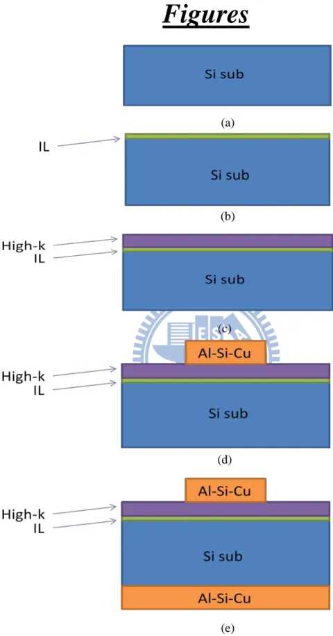
Fig. 2.1. Key fabrication steps of an MOS capacitor. (a) Start with a bare silicon substrate. (b) Formation of an interfacial layer by RTO. (c) Deposition of a high-κ layer by ALD and PDA. (d) Top electrode deposition and patterning. (e) Back electrode deposition. ………... 43 Fig. 2.2. (a) Equivalent circuit of a MOS capacitor including series resistance
s R .
(b) Simplified version of (a). ……….. 44
Fig. 2.3. (a) C-V plots of an MOS capacitor measured at different frequencies. (b) C-V plots of the corrected data. ……….……….. 45 Fig. 2.3. (c) G-V plots of an MOS capacitor measured at different frequencies. (d)
G-V plots of the corrected data. ……….……….. 46 Fig. 2.4. XRD data for the HfO2 samples of (a) 5 nm and (b) 10 nm thickness. ….. 47
Fig. 2.5. (a) C-V and (b) J-V curves of 5 nm-Al2O3 samples with various PDA
conditions. ……… 48 Fig. 2.6. (a) C-V and (b) J-V curves of 5 nm-Al2O3 samples with various PDA
conditions. ………..……. 49 Fig. 2.7. (a) C-V and (b) J-V curve of 5 nm-HfO2 samples with various PDA
conditions. ……… 50 Fig. 2.8. (a) C-V and (b) J-V curve of 10 nm-HfO2 samples with various PDA
conditions. ……… 51 Fig. 2.9. Schematic showing different types of charges presenting in the silicon
dioxide/Si system [2-14]. …….……… 52 Fig. 2.10. The extracted interface states density of (a) 5 nm and (b) 10 nm HfO2
samples annealed at different temperatures for 30 sec. ………... 53 Fig. 2.11. The extracted hysteresis window size for HfO2 samples of different
thicknesses. ……… 54
Chapter 3
Fig. 3.2. (a)Top view and (b) cross-sectional view of the NW devices. ………..…… 56
Fig. 3.3. Key process flow of the NW devices. ……… 57
Fig. 3.4. Cross-sectional TEM pictures of (a) NW-TONOS, (b) NW-TAHOS, (c) MOS-MANOS, (d) MOS-MAHOS-A, and (e) MOS-MAHOS-C devices. . 59
Fig. 3.5. XRD data of the dielectric films in MOS devices. ………. 62
Fig. 3.6. Basic C-V curves of the MOS capacitors (the capacitance has been normalized to the area). ………. 62 Fig. 3.7. C-V curves of MOS capacitors measured with a sweeping Vg range of (a)
±10 V and (b) ±15 V. ………. 63 Fig. 3.8. Band diagrams under a positive bias of (a) MONOS, (b) MANOS, and (c)
MAHOS capacitors. ………..……… 64 Fig. 3.9. C-V plots of the samples before and after applying a positive gate bias for
60 s. (a) MONOS, (b) MANOS, (c) MAHOS-A, (d) MAHOS-B, (e) MAHOS-C, (f) MAHOS-D. ………. 66 Fig. 3.10. Transfer characteristics of the fabricated devices. ……….………... 69 Fig. 3.11. Transfer I-V curves of a TANOS device after (a) programming and (b)
erasing operation with the positive and negative bias conditions, respectively. ………...……… 70 Fig. 3.12. (a) Programming and (b) erasing characteristics of NW-TONOS devices
with different gate biases. ……….……… 71 Fig. 3.13. (a) Programming and (b) erasing characteristics of NW-TANOS devices
with different gate biases. ……….……… 72 Fig. 3.14. (a) Programming and (b) erasing characteristics of NW-TAHOS devices
with different gate biases. ……….……… 73 Fig. 3.15. Schematic band diagrams of (a) TONOS, (b) TANOS, and (c) TAHOS
devices under a positive programming bias. ……….……… 74 Fig. 3.16. Comparisons of programming characteristics of the three types of devices
under the same programming bias. ……… 75 Fig. 3.17. Schematic band diagrams of (a) TONOS, (b) TANOS, and (c) TAHOS
devices under a negative erasing bias. ……… 76 Fig. 3.18. Erasing comparisons of the three devices under the same erase bias. …… 77 Fig. 3.19. (a) Programming and (b) erasing characteristics of TAHOS devices with
Fig. 3.20. Charge loss paths under the retention condition. ……….……. 79 Fig. 3.21. Retention characteristics of the three types of devices. ………...……. 79 Fig. 3.22. Endurance characteristics of the TONOS and TAHOS devices. …………. 80 Fig. 3.23. I-V plots of the (a) TONOS and (b) TAHOS devices with increasing P/E
List of Tables
Chapter 2
Table 2.1. Potential candidates for gate dielectric of future CMOS technology. .…… 17
Table 2.2. Split table for MOS capacitors. ……….………... 17
Chapter 3
Table 3.1. Film composition of different splits of the MOS capacitors. ……….. 32 Table 3.2. Measured accumulation capacitance, CET, and estimated CET. ……..….. 32 Table 3.3. Hysteresis window of the MOS capacitors with different sweeping
voltage ranges. ………. 32 Table 3.4. Memory window and the extracted charge density from the results shown
Chapter 1
Introduction
1-1 Overview of Multiple Gate Structures and
Nanowires
The state-of-the-art technology node of semiconductor manufacturing is 28 nm
and on the way to 22 nm. As the device scales down to nano scale, the worsened
threshold voltage roll-off and degraded subthreshold swing phenomena due to lateral
electric field penetration from the drain, known as the short-channel-effects (SCEs),
are becoming increasingly more difficult to keep at bay. In order to suppress the SCEs,
the adoption of multiple-gated (MG) structures presents a feasible and promising way
to enhance the gate controllability [1-5]. A large number of studies and development
works on MG structures have been launched, such as double-gated FinFET [1-1],
tri-gated (TG) FETs [1-2], Ω-gated FETs [1-3], and gate-all-around (GAA) structures [1-4][1-6][1-8]. In the above-mentioned structures, GAA is demonstrated to be the
most ideal configuration considering the channel electrostatic controllability
[1-6][1-7][1-8].
a range of device functions and at the same time serve as bridging wires. By taking
advantage of the high surface-to-volume ratio inherent in a NW structure, the carrier
transport in it would be promptly influenced by the surface condition. Such a feature
opens up many exciting opportunities for numerous applications. For example, Y. Cui
et al. [1-9] have developed nanowire for high performance field-effect transistors. F.
Patolsky et al. [1-10] and Y. Cui et al. [1-11] have used nanowire transistors as
biological and chemical sensors because of their high sensitivity. A NW is also
attractive for memory devices because it can provide higher program/erase efficiency
and low voltage operation [1-12].
1-2 Overview of SONOS Flash Memory
Data storage market based on NAND-type flash memory devices has grown
explosively in recent years because of the increasing demands of portable electronic
products. Because the data can be retained when power is switched off, NAND-type
flash memory is widely employed in numerous portable products such as iphone, ipad,
digital cameras, and mp3 players etc. In addition, the fabrication process is
compatible with the mainstream CMOS process, making it easily integratable in
electronic systems. In recent years, nonvolatile memory (NVM) devices are moving
reliability [1-13]. In this regard, the scaling of NAND-type flash memory has been
aggressively pursued in recent years [1-14]. Although floating-gate (FG) flash
memory is still the work horse of the market today, FG flash memory devices are
vulnerable to single defect in the tunnel oxide which could result in fatal data loss
[1-15]. This, together with the FG coupling issue [1-16], has seriously limited the
future scaling of the FG devices. Recently, the SONOS devices have thus emerged as
a potential candidate for replacing the FG devices as the future main-stream NVM
due to their inherent merits, such as the capability of using thinner tunnel oxide and
thus lower operation voltage, and the immunity to gate coupling issue [1-17]. The
main difference between FG and SONOS devices is the type of charge storage
medium. Unlike conventional FG devices, the electrons are stored in discrete traps of
nitride-based dielectric in SONOS and are not susceptible to the defects in the tunnel
oxide generated during operation. Hence the SONOS exhibits better tunnel oxide
reliability than FG [1-18].
Today, polycrystalline thin film transistors (poly-Si TFTs) SONOS have attracted
much attention for the purpose of high density storage applications [1-19]. However,
there are still some challenges to be addressed such as low memory speed and poor
subthreshold swing (S.S.) in poly-Si TFTs [1-20]. By utilizing nanowire (NW) TFT
achieved [1-20]. Improved NVM characteristics have also been demonstrated in
poly-Si NW SONOS-TFTs [1-20]. Such SONOS-TFT is thereby highly promising for
future system-on-panel display applications.
1-3 Overview of High-
κ Applications
As the FG NVM facing the scaling limit, the SONOS memory has turned out to
attract much attention. However, there still exist some issues in scaling for the
SONOS [1-20]. For example, although a thicker tunnel oxide is more reliable in
retention, it would degrade the erase efficiency. Although band-to-band tunneling hot
hole injection (BTBHHI) is effective for erasing with thick tunnel oxide, it is not
suitable for NAND-type Flash as it makes the device vulnerable to the side effects
brought about by the hot holes [1-21]. For higher program/erase efficiency, an
ultra-thin tunnel oxide is preferable. However, thinner tunnel oxide will cause data
retention concern [1-18]. Such a dilemma could be addressed with the implementation
of high-κ materials and metal gate electrodes [1-22]. In order to achieve faster memory characteristics, a substantial amount of research works have been established
on MONOS (Metal-SiO2-Si3N4-SiO2-Silicon)-type memory devices [1-14], including
engineering of gate electrode [1-23], blocking oxide [1-23][1-24], trapping layer
charges are stored in discrete traps of the storage medium. High dielectric constant
(high-κ) materials such as HfO2 [1-20], Al2O3 [1-28], La2O3 [1-29] and ZrO2 [1-30]
are known to possess higher trap density, and thus considered as suitable materials for
charge-trapping layers. On the other hand, gate injection electron current is
undesirable during erase operation, so high-κ materials like Al2O3 is adopted to reduce
the electric field across the blocking oxide. Finally, the adoption of high work
function metal gates increases the barrier height for electrons and hence also reduces
the electron injection probability from the gate. From this point of view, metal gate
electrodes such as TiN and TaN with a work function higher than the commonly-used
n+-poly-Si are widely employed [1-26][1-31]. By combining the above advantages, a new device called TAHOS (TiN-Al2O3-HfO2-SiO2-Si) structure has been proposed for
next-generation NVM devices [1-32]. The utilization of high-κ dielectrics in such a scheme will further reduce the effective-oxide-thickness (EOT) and favors the device
scaling trend.
1-4 Motivation
For the next-generation flash memory, high operation speed and high density are
desirable. As have been pointed out in previous work [1-33], a nanowire transistor
reliability concerns. But the memory window may be limited by the nitride-based
charge trapping mechanism. So in this thesis we explore the feasibility of using high-κ materials as an alternative and hope to find some useful candidates which contain
high trap density to improve the memory window. Moreover, owing to the inherent
characteristics of high dielectric constant materials, operation speed can be improved
because of the thinner EOT. To further promote the device performance, we also
employ high work function metal gate to reduce the gate injection current during the
erasing process. Accordingly, SONOS-like charge trap memory devices with
combination of the above-mentioned features are fabricated and characterized in this
study with an aim at improving the memory characteristics.
1-5 Organization of this Thesis
In this thesis, a general background of polysilicon nanowire transistors, SONOS
memory and high-κ materials are introduced in Chapter 1. In Chapter 2, we investigate devices with a simple MOS structure to investigate the characteristics of
high-κ materials. In Chapter 3, a TAHOS nanowire transistor is presented, and we will discuss the memory characteristics of the fabricated devices. In Chapter 4, we will
summarize all we observed and make brief conclusions. Finally, some suggestion will
Chapter 2
Fabrication and Characterization
of High-
κ MOS Capacitors
2-1 Brief Introduction of Atomic Layer Deposition
Recently, the scaling of complementary metal-oxide-semiconductor (CMOS)
transistors has reached nano-scale regime, which requires ultra-thin gate silicon
dioxide (SiO2) to obtain desirable device performance. However, continuous
shrinkage of the silicon dioxide would lead to undesirable gate leakage current.
Accordingly, it is necessary to look for new materials with higher dielectric constant (κ) to replace the conventional SiO2 with a physically thicker layer. A list of
promising candidates is shown in Table 2.1 [2-1]. For the demand of ultra thin oxide
and thickness uniformity, atomic-layer-deposition (ALD) has been adopted to meet
these requirements. ALD was first developed in the 1970s with the name of
atomic-layer-epitaxy (ALE), and was used for thin-film electroluminescent (TFEL)
flat panel applications [2-2]. Nowadays ALD is getting more attraction as a result of
decreasing device dimensions and increasing aspect ratio in integrated circuits (ICs),
due to its excellent surface control and self-limiting growth mechanism.
The growth of ALD is composed of alternate pulsing of the precursor gases onto
purged with an inert gas between the precursor pulses. Therefore, a typical ALD
process can be simply described as follows: (a) Exposure of the first precursor, (b)
purge of the reaction chamber, (c) exposure of the second precursor, and (d) a further
purge of the reaction chamber. These four basic steps constitute one cycle of ALD
process, and only a monolayer will be deposited in one cycle. So the film thickness
can be accurately controlled by this self-limiting mechanism. Another advantage of
ALD is the superior step coverage which is conducive to excellent conformal
deposition on extremely non-planar surface topographies [2-3, 2-4, 2-5]. Owing to
these inherent characteristics of ALD, it becomes a promising candidate in nano-scale
IC processing. In this thesis, we employed ALD in our process for a precise thickness
control of high-κ layers.
2-2 Device Structure and Process Flow of the MOS
Capacitors
In this thesis, we utilized a simple metal-oxide-silicon (MOS) structure to
investigate the characteristics of high-κ layers. First, we used 6-inch p-type (100) bare silicon wafers as starting substrates [Fig. 2.1(a)], with resistivity in the range of 2 to 7 Ω‧cm. After RCA clean, the wafers received a rapid-thermal-oxidation (RTO) at 500
o
C for 10 sec to form an interfacial layer [Fig. 2.1 (b)]. The thickness of the interfacial
layer is approximately 1 nm as measured by an ellipsometer. In the subsequent step,
we used an ALD system to deposit the high-κ layer immediately [Fig. 2.1(c)]. For studying the influence of different post-deposition-anneal (PDA) temperatures, we
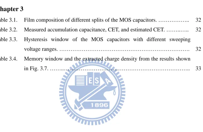
manufactured different splits of samples. The detailed experiment split table is shown
500 nm as the top gate material, followed by a photolithographic step to generate
phototresist patterns of gate electrodes, and then using a mixture of acetic acid,
phosphoric acid, and nitric acid to remove the exposed Al-Si-Cu and define the gate
electrode [Fig. 2.1(d)]. In the final step, we also employed PVD to deposit Al-Si-Cu
of 500 nm to serve as the back electrode [Fig. 2.1(e)] to accomplish the MOS
capacitors. Capacitance-voltage (C-V) and current-voltage (I-V) measurements were
then utilized to probe the characteristics of the high-κ layers.
2-3 Measurement Setup and Electrical
Characterization
The C-V and I-V characteristics were evaluated by an automated measurement
setup constructed by HP 4156A and Agilent 4284A precision semiconductor
parameter analyzers, Agilent TM 5250A switch, and the Interactive Characterization
Software (ICS). During the measurements, the temperature was controlled at a stable
value by a temperature-regulated chuck.
During the C-V measurements, because of the concern of high leakage current
from the high-κ layer, we adopted parallel equivalent circuit model. The frequency of measured capacitance was varied from 5k to 500k Hz. After the measurements, we
used the following equation to extract the capacitance-equivalent-thickness (CET) of
the high-κ layers,
0 2 . SiO acc A CET C ε ε = . (Eq. 2-1)
In the above equation, A means the area of the measured capacitor, and the value is
capacitor. ε0 and εSiO2 indicate the permittivity of vacuum and silicon dioxide, respectively. We also measured the gate leakage current density of the capacitor to
analyze the influence of different PDA temperatures.
On the other hand, as a high series resistance, Rs, exists in the capacitor, the
measured capacitance would have a deviation from the true oxide capacitance [Fig.
2.2] [2-6]. This deviation is getting larger with increasing measurement frequency
[Fig. 2.3 (a)]. This effect can be resolved by using the following equations to calibrate
the measurement results:
2 2 2 2 2 2 ( m m ) m c m G C C C a C ω ω + = + , (Eq. 2-2) and 2 2 2 2 2 2 ( m m ) c m G C a G a C ω ω + = + , (Eq. 2-3)
where Cc, Cm, Gc, Gm are the calibrated capacitance, measured capacitance, calibrated
conductance, and measured conductance, respectively, is the frequency, and
2 2 2
( )
m m m s
a=G − G +ω C R . R can be written as the following equation: s
2 2 ( ) acc s acc acc G R G ωC = + . (Eq. 2-4)
Here we use the MOS capacitor with HfO2 of 5 nm and annealing at 500 oC for 30 s
as an example [Fig. 2.3 (a)~(d)]. As we can see, the capacitance and conductance are
strongly affected by the series resistance [Figs. 2.3 (a), (c)]. After calibration,
difference among the capacitances measured at different frequencies would become
much smaller [Fig. 2.3 (b)], and the lost conductance peak in Fig. 2.3 (c) appears
again [Fig. 2.3 (d)]. The re-appearance of normal conductance characteristics allows
us to extract the interface trap density. The conductance method was first proposed by
frequency approach for interface-state density approximation in 1980 [2-8]. We used
the following equation to extract the interface trap density [2-9],
,max 2 2 ,max / 2 [( / ) (1 / ) ] c it c ox c ox G D qA G C C C ω ω = + − . (Eq. 2-5)
Here, Gm,maxindicates the maximal value of the measured conductance, and C is c
the corrected capacitance along with theGc,max.
In addition, we also measured the hysteresis phenomena to study the trapping
characteristics of the high-κ layers. The measurement was executed by first sweeping gate voltage from 3 V to -3 V and then sweeping back to 3 V.
2-4 Device Characteristics of MOS Capacitors
2-4.1
Basic Material Analyses
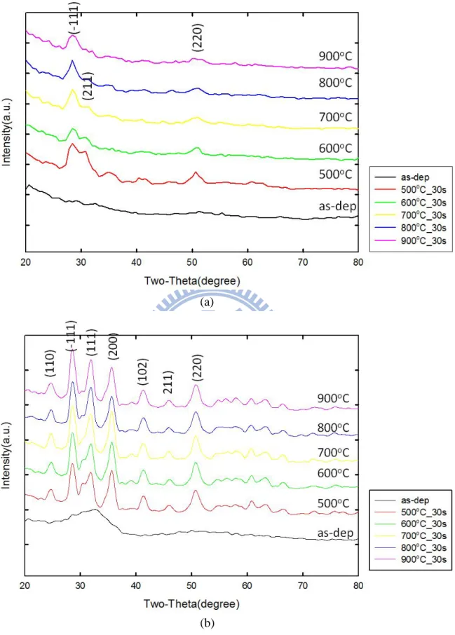
First, we utilized X-ray diffraction (XRD) to characterize the micro-structural
properties of the HfO2 samples with various film thickness and PDA temperature. As
shown in Fig. 2.4, the as-deposited samples appear to be amorphous in nature as
expected, while the annealed samples show evidence of the crystalline phase. This
phenomenon has received much attention because the adoption of high-κ materials is an important topic for IC industry in recent years [2-10]. It is clearly found that the
PDA temperature exhibits strong influence on the crystalline properties of the HfO2
films. That is, the film exhibits more crystalline phases with increasing PDA
temperature. It is also noteworthy that for the thicker HfO2, the XRD results reveal
more crystalline phases, possibly due to more nucleation sites contained in the thicker
aggravate gate leakage. But this phenomenon could be beneficial for memory
applications, as will be discussed in the following sections.
2-4.2
Fundamental J-V and C-V Characteristics of MOS
Capacitors
In this section, we used the samples in Table 2.2 to explore the influences of
PDA temperature and duration. The capacitance value was corrected by the series
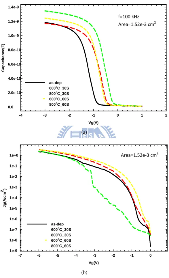
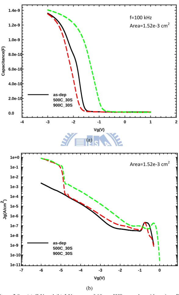
resistance effect as mentioned in Section 2-3. First, the samples of Al2O3 films with
thickness of 5 nm were examined. The capacitance is found to increase with the
annealing temperature [Fig. 2.5 (a)], which could be ascribed to the defect repairing
during annealing. Accordingly, as the dielectric becomes more robust, the gate
leakage current reduces. A dramatic improvement of gate leakage is indeed observed
for the sample receiving 900 oC-30 sec annealing as compared with the as-deposited one [Fig. 2.5 (b)]. When we extend the annealing duration to 60 sec, the capacitance
can be further raised [Fig. 2.6 (a)]. This indicates that the annealing time is also an
important concern for the film quality. However, the leakage current increases as the
annealing time is increased from 30 to 60 sec, as depicted in Fig. 2.6 (b). This may be
due to the occurrence of the Al2O3 film crystallization with longer annealing time.
Extra leakage current paths likely appear at the crystallized grain boundaries [2-11].
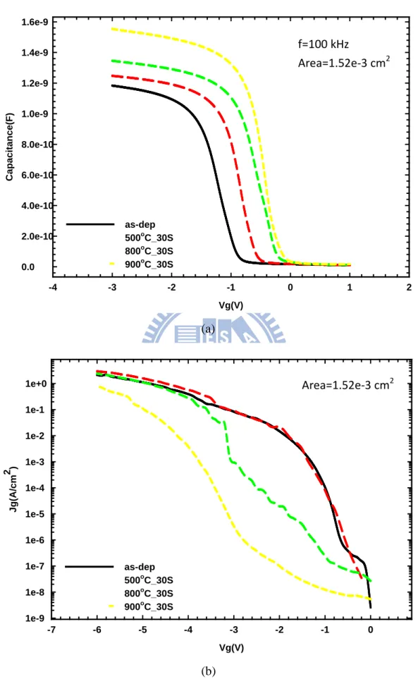
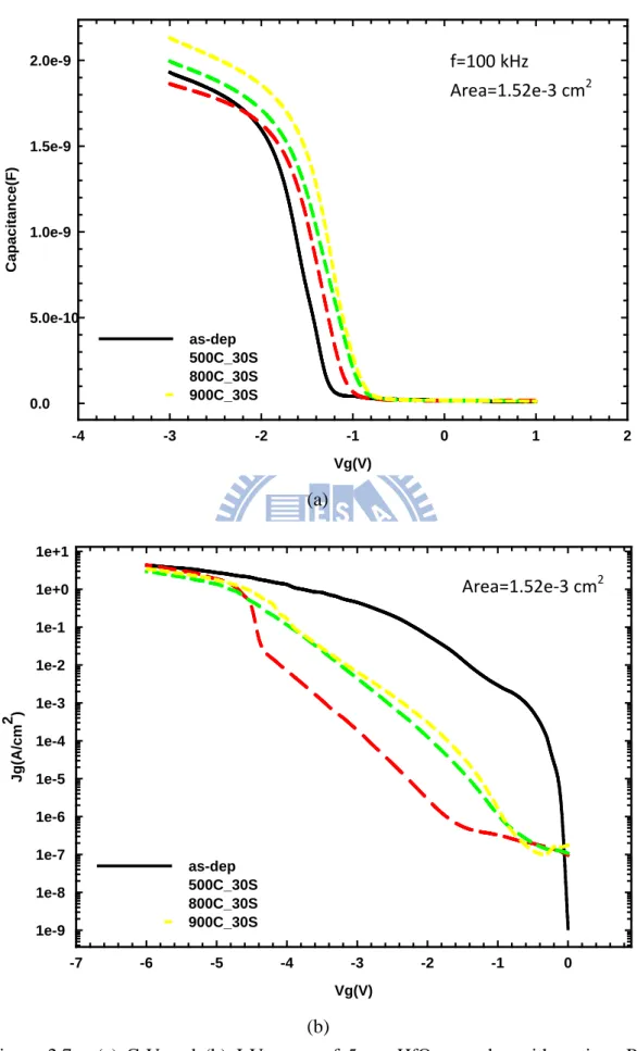
Moreover, the samples with 5 nm-HfO2 are also investigated. As the C-V curves
shown in Fig. 2.7 (a), the as-deposited film shows higher capacitance than the sample
with 500 oC-30 sec annealing, which may be resulted from the oxygen diffusion to the interface during the annealing, thus leading to a thicker interfacial layer. However, as
attributed to the improved film quality with higher dielectric constant [Fig. 2.7 (a)].
On the other hand, the J-V curves in Fig. 2.7(b) exhibit higher leakage current for the
as-deposited film, compared with the samples receiving high temperature annealing,
which can be ascribed to the interfacial layer growth effect, [2-12]. Nevertheless,
when comparing the samples receiving different annealing temperatures, a slightly
increased leakage current with higher PDA temperature is observed. Higher
temperature also favors film crystallization, as shown in Fig. 2.4, and therefore
resulting in a higher leakage [2-13]. For a thicker sample (10 nm), the trends in C-V
characteristics [Fig. 2.8 (a)] are similar to those observed in [Fig. 2.7 (a)]. But it is
interesting to see that the leakage current of the as-deposited sample is lower than the
annealed ones [Fig. 2.8 (b)]. This implies that the film crystallization extent turns out
to be the dominant factor in the present case, which is also evidenced from the XRD
results as revealed in Fig. 2.4.
2-4.3
Analyses of Interface States and Hysteresis Phenomena
Thermally grown SiO2 is usually treated as an ideal dielectric when contacting
with the silicon substrate. Actually, the measured electrical characteristics are affected
by some positive charges near the silicon/SiO2 interface or trap charges in the bulk
oxide. Other types of charges are either positive or negative ones trapped by interface
states and mobile ionic charges which are generated during the fabrication process
[2-14]. The electrical properties of devices are very sensitive to the interface state
density ( D ). The interface states are located at or very close to the it
semiconductor. These states may trap electrons or holes at the interface and then
become charged. All the charged states can be taken as interface charges (Qit). When
a high-κ material is used as the gate dielectric, the concern of interface state becomes more important. Moreover, formation of the interfacial layers is usually inevitable
when using high-κ materials in semiconductor fabrication because of the existence of high temperature process step in the following manufacturing procedure. When
high-κ materials are first introduced, people simply accept such interfacial layer that grows naturally after the deposition of high-κ materials. But in recent years, it has been recognized that high Dit associated with such interfacial layer will seriously
aggravate the electrical properties. In line of this, nowadays people are apt to
intentionally deposit an interfacial layer with desirable quality before the high-κ film deposition [2-15]. In our experiment, a RTO oxide layer was formed prior to the
high-κ film deposition. The forming condition was conducted in O2 (with 10 % N2)
atmosphere at 500 oC for 10 s. And then the Dit was extracted by the conductance
method with single frequency approximation [2-5]. Just like many data proposed
before, the Ditof as-deposited HfO2 is in the order of 1E12 to 1E13(eV-1cm-2) [2-16].
After the PDA treatment, the Dit decreases significantly [Fig. 2.10]. Although the
major gas is N2 during PDA, there still exists approximately 5 % O2 presenting in the
chamber. It is possible that the oxygen can diffuse to the interface to improve the
interface quality. When the temperature rises from 500 oC to 800 oC, the Dit increases
slightly.This may result from the fact that the coefficient of thermal expansion (CTE)
of HfO2 (6.5 10 K× −6 −1) [2-17] is much larger than that of SiO2 (0.5 10 K× −6 −1) [2-18]
or Si (2.6 10 K× −6 −1) [2-18]. And another possibility is the diffusion of impurities or defects to this interface [2-19]. Furthermore, the oxygen compensating phenomenon is
lowest Ditcan be achieved (6×10¹¹ ev-1cm-2) among all the samples.
As abovementioned, there are many kinds of charges in the oxide or
oxide/silicon surface. Owing to the innate high defect density, a transistor with high-κ materials tends to have flat-band voltage shift after forward and backward gate
voltage sweeping, which is usually called the hysteresis [2-20]. This phenomenon is
undesirable for fundamental logic devices but can be exploited for nonvolatile
memory applications because of its capability of trapping charges. Therefore, in order
to use HfO2 as the charge trapping layer, we preliminarily investigate the hysteresis
characteristics of the HfO2 capacitor samples with three different thicknesses. In the
measurement, all the samples were operated with the gate bias sweeping from
inversion to accumulation and then backward. The sweeping voltage range is ±3 V.
We found that the hysteresis increases with increasing film thickness, implying that
the number of trapping sites increases with film thickness. Next, the influence of PDA
will be discussed. From the XRD data, the HfO2 films have shown signs of
crystallization even with the low annealing temperature of 500 oC. The hysteresis of the 5 nm and 10 nm as-deposited samples are 132 mV and 518 mV, respectively.
After 500 oC-30 sec PDA treatment, the values increase to 270 mV and 840 mV, respectively [Fig 2.11]. This might be due to the incomplete film crystallization
during the PDA process and thus more trapping sites generated at intra/inter grains.
Another interesting thing is that the hysteresis decreases when we further raise the
annealing temperature. From the XRD data, some grain orientations disappear as the
annealing temperature is higher. This means the grains became larger at the higher
annealing temperature. Therefore, some crystalline defects could be significantly
2-5
Summary
In this chapter, fundamental material and electrical characteristics of high–κ materials are studied. We have successfully fabricated and characterized MOS
capacitors with HfO2 or Al2O3 dielectric of different thicknesses. The crystallization
of HfO2 after high temperature annealing was confirmed by XRD data. For Al2O3
samples, the crystallization-free annealing temperature could be as high as 800 oC without causing a high gate leakage. When the annealing time is extended to 60 sec,
the dielectric constant can reach a higher value, suggesting the improved film quality.
On the other hand, the HfO2 samples seem to be more vulnerable to the PDA
treatment. Annealing at 500 oC and higher temperatures could reduce the gate leakage significantly owing to more pronounced interfacial layer re-growth for 5 nm-HfO2
samples. But the HfO2 thin films also become crystallized during the annealing and
the gate leakage is closely affected by the annealing, especially for the thicker HfO2
samples. Dit and hysteresis effects were also probed to discuss the influence of
annealing temperature. Based on these results, we opt for 600 oC/30 sec annealing condition for the high-κ based memory devices and the device characteristics are presented and discussed in Chapter 3.
Tables
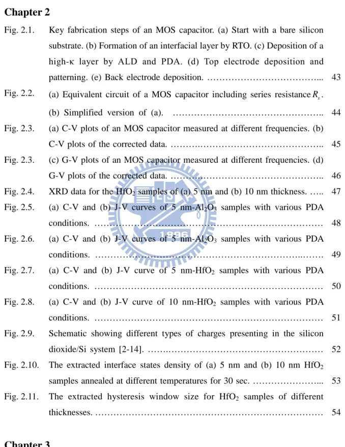
Table 2.1. Potential candidates for gate dielectric of future CMOS technology.
κ Band Gap (eV) CB offset (eV)
Si 1.1 SiO2 3.9 9 3.2 Si3N4 7 5.3 2.4 Al2O3 9 8.8 2.8 Ta2O5 22 4.4 0.35 TiO2 80 3.5 0 SrTiO3 2000 3.2 0 ZrO2 25 5.8 1.5 HfO2 25 5.8 1.4 HfSiO4 11 6.5 1.8 La2O3 30 6 2.3 Y2O3 15 6 2.3 a-LaAlO3 30 5.6 1.8
Table 2.2. Split table for MOS capacitors.
HfO2 Al2O3 5 nm 10 nm 15 nm 5 nm 10 nm PDA ◆ ◆ ◆ ◆ ◆ 500℃,30s ◆ ◆ ◆ 600℃,30s ◆ ◆ ◆ ◆ 700℃,30s ◆ ◆ ◆ 800℃,30s ◆ ◆ ◆ ◆ 900℃,30s ◆ ◆ ◆ 500℃,60s ◆ 600℃,60s ◆ ◆ ◆ 700℃,60s ◆ ◆ 800℃,60s ◆ ◆
Chapter 3
Fabrication and Characterization
of MAHOS MOS Capacitors and
TAHOS NW-Channel TFTs
3-1 Device Structure and Process Flow for
Fabricating the MAHOS Capacitors
The structure and layout are the same as those mentioned in Chapter 2, so the
description below is brief. The process flows for fabricating different types of
capacitors are shown in Fig. 3.1. 6-inch p-type (100) bare silicon wafers were used as
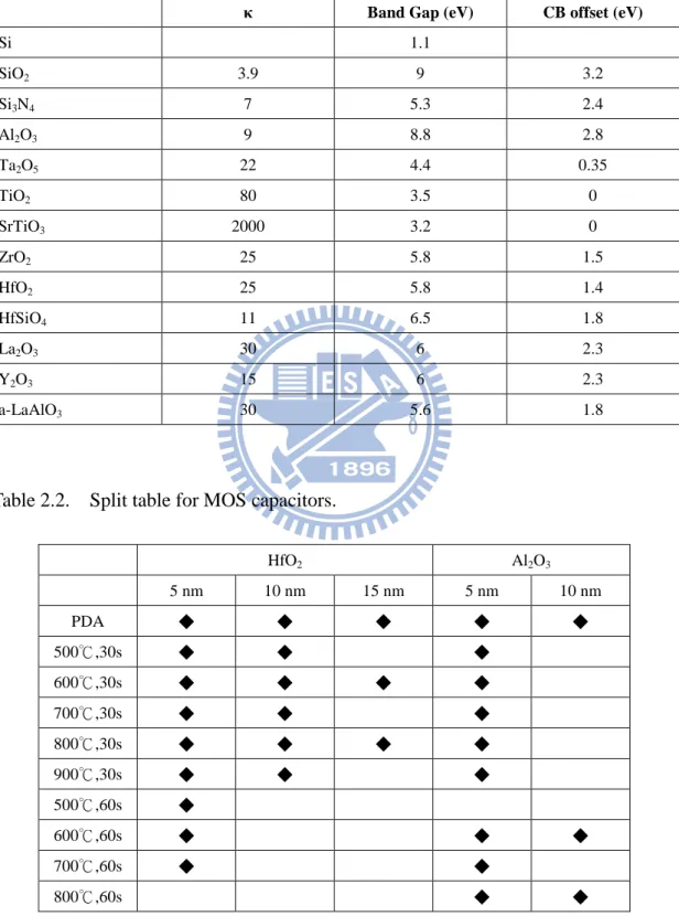
starting substrates [Fig. 3.1(a)], with resistivity ranging from 2 to 7 Ω‧cm. Three major structures, namely, MONOS, MANOS, MAHOS, were fabricated and
characterized in this experiment and details about the dielectric composition of the
splits are shown in Table 3.1. In the MAHOS structure, HfO2 films deposited at
different temperatures are specifically addressed. The major objectives are to reduce
the thermal budget and increase the trapping sites in the trapping layer. After RCA
deposit TEOS oxide with nominal thickness of 3 nm as the tunnel oxide in all devices
[Fig. 3.1 (b)]. Afterwards, the atomic layer deposition (ALD) HfO2 or LPCVD nitride
serving as the trapping layer and ALD Al2O3 or LPCVD oxide serving as the block
oxide were deposited subsequently [Fig. 3.1 (b)]. Then, physical vapor deposition
(PVD) was used to deposit 500 nm-thick Al-Si-Cu as the top gate electrode [Fig. 3.1
(c)]. The final step was the deposition of PVD Al-Si-Cu with thickness of 500 nm as
the back electrode [Fig. 3.1 (d)].
3-2 Device Structure and Process Flow of the
TAHOS NW-TFTs
Fig. 3.2 shows the top and cross-sectional views of the fabricated SONOS-type
poly-Si NWFET with gate-all-around (GAA) structure. It can be seen that the NW
channels are surrounded by the gate. Figs. 3.3(a) ~ (k) depict the major process steps
of fabricating the devices. All devices in this work were fabricated on 6-inch bare
silicon wafers capped with a 200 nm-thick wet oxide. First, a 40 nm bottom nitride
layer was deposited by LPVCD. Then, a 40 nm TEOS oxide and a 30 nm nitride
dummy layer (hard mask layer) were deposited sequentially [Fig. 3.3 (a)]. After a
standard I-line lithographic step, the nitride/TEOS dummy layer was patterned by
anisotropic reactive plasma etching [Fig. 3.3 (b)]. In this etching step, the etching time
was carefully controlled to stop right on the top of the bottom nitride layer. Then, we
used diluted HF (DHF) to etch the dummy structure and form rectangular-shaped
cavities at both sides of the dummy patterns [Fig. 3.3 (c)]. Note that the size of NW
channels could be adjusted by controlling the etching time. After forming the cavities,
channel material [Fig. 3.3 (d)]. Afterwards, an annealing step was performed at 600
o
C in N2 ambient for 24 hours to transform the α-Si into polycrystalline phase [Fig.
3.3 (e)]. Then by adopting a dry etching step with endpoint detection, the NW
channels were formed in the cavities [Fig. 3.3 (f)]. Subsequently, in situ
phosphorus-doped poly-Si was deposited by LPCVD at 550 ◦C and 600 mtorr with the PH3 flux of 15 sccm [Fig. 3.3 (g)]. Then S/D patterns were defined through an I-line
stepper, followed by an anisotropic dry etching step to define S/D [Fig. 3.3 (h)]. It
should be noted that the devices whose S/D regions are formed by employing in situ
doping technique show better performance than those formed by ion-implanted
poly-Si [3-1]. Afterwards, wet etch steps were used to remove the nitride layer and
dummy TEOS with hot H3PO4 and DHF, respectively. In order to form the suspended
NW channels hanging between the S/D regions, the bottom nitride was completely
stripped off by hot H3PO4 [Fig. 3.3 (i)]. All wafers were then deposited with a 3 nm
TEOS oxide as the tunnel oxide. Wafers were then split to form the three major
structures in our experiment, For TONOS and TANOS structures, a 7 nm silicon
nitride layer was deposited as the trapping layer after the tunnel oxide deposition. The
TONOS device was then deposited with a 12 nm TEOS oxide which serves as the
block oxide subsequently. For TANOS device, a 12 nm-thick ALD Al2O3 was
deposited as the block oxide. While for devices of the third type, ALD was used to
sequentially deposit HfO2 and Al2O3 as the trapping layer and block oxide,
respectively, after the tunnel oxide deposition [Fig. 3.3 (j)]. In this structure, the
deposition temperature of HfO2 was varied from 250oC to 100oC to study its effects
on the TAHOS device characteristics. The process conditions are summarized in
Table 3.1. Afterwards, a 6 nm TiN was deposited with ALD to serve as the gate for all
channel is surrounded by the gate. Next, we adopted PVD to further deposit a TiN of
150 nm to complete the gate electrode. After depositing a 500 nm passivation oxide
layer and opening contact holes, a standard metallization step was performed to
complete the device fabrication.
3-3 Basic Material Analysis
In this section, we investigate the structural characteristics of the fabricated
devices, including MOS capacitors and NWs. All devices with high-κ layers were subjected to a 600oC-30s annealing step. TEM pictures and XRD were employed as the analysis method. Fig. 3.4 (a) is the TEM picture of a TONOS structure and Fig.
3.4 (b) is for a TAHOS device. Because the etching rate is not controlled precisely,
the NW dimension is larger than our expectation (actual size is shown in the TEM
picture). For the rectangular-shaped NW, the corner will enhance the electric field and
affect the electrical characteristics which will be discussed later. Figs. 3.4 (c) ~ (e)
depict the TEM images of MOS capacitor stacks. It is obvious that the HfO2 is
evidently crystallized for all the deposition temperatures used. The most interesting
thing is that the Al2O3 film retains its amorphous nature in the MANOS structure [Fig.
3.4 (c)]. In contrast, the Al2O3 film in the MAHOS structure is crystallized evidently
[Figs. 3.4 (d) & (e)]. The reason is presumably due to the underneath crystallized
HfO2 which helps the crystallization of Al2O3 in some specific direction. Combining
the TEM pictures and XRD data [Fig. 3.5] , the crystalline nature of HfO2 can be
easily proofed. In the XRD data, we can find out that the samples deposited at a lower
deposition temperature exhibit more crystallization textures. According to the results
we discussed in Chapter 2, samples deposited at a lower temperature could contain
achieve larger memory window.
3-4 Analysis of Nonvolatile Memory Capacitors
3-4.1 Measurement Setup
The capacitance-voltage (C-V) characteristics were evaluated by an automated
measurement setup constructed by Agilent 4284A precision semiconductor parameter
analyzer, an Aglient TM 5250A switch, a pulse generator Agilent-81110A, and the
Interactive Characterization Software (ICS). During all measurements, the
temperature was controlled at a stable value by a temperature-regulated chuck. For
basic C-V measurements, we adopted a parallel equivalent circuit model. The
frequency of the measured capacitance was set at 100k Hz. After the measurement of
capacitance, the following equation was used to extract the
capacitance-equivalent-thickness (CET) of the capacitor:
0 2 . SiO acc A CET C ε ε = . (Eq. 3-1)
On the above equation, A means the area of the measured capacitor, and the
value is assumed to be 1.52×10⁻³ cm2 here. Cacc. represents the accumulation capacitance of the capacitor. ε0 and εSiO2 indicate the permittivity of vacuum and silicon dioxide, respectively.
3-4.2
Basic Capacitance-Voltage Analysis
Fig. 3.6 depicts the C-V curves of all devices. The measurements were conducted
from inversion to accumulation conditions. The accumulation capacitance and
capacitance than MONOS owing to the higher permittivity of Al2O3. The permittivity
of Al2O3 is nearly 8 based on the result presented in Chapter 2. MAHOS devices
exhibit higher capacitance than other two structures. This comes from the contribution
of HfO2 whose permittivity is nearly 16. We can verify the measured CET by the
following equation:. 2( ) TO TL BO SiO TO TL BO t t t CET ε ε ε ε = + + . (Eq. 3-2)
The calculated CET values are shown in Table 3.2, and the results are close to
the measured ones. Looking at the plots in Fig. 3.5 carefully, small differences in
acc
C can be found among the MAHOS-A ~ D samples. These differences can be an
indication that the deposition temperature of ALD chamber would more or less
influence the film quality of HfO2 [3-2]. Another important thing that should be noted
is the flat-band voltage differences among all samples. A former study on hafnium
oxide has shown that the oxygen vacancy defects could present in HfO2 [3-3]. The
flat-band voltage shift is mainly caused by the positive fixed oxide charge (Q ) ot
which is related to the oxygen vacancies formed during the process. The quantities of
oxygen vacancy rise when the deposition temperature decreases.
3-4.3 Nonvolatile Memory Characteristics
In this section, two kinds of memory characteristics are evaluated with planar
MOS capacitors. The first one is the hysteresis effect. We use a wide round-trip
sweeping voltage range to estimate the trapping efficiency of the capacitors. The
results are shown in Fig. 3.7 and Table 3.3. Conventional O/N/O stack depicts the
there’s an obvious difference in the memory window. The main reason is postulated to
be due to the excessive charge trapping sites presenting in the Al2O3 or Al2O3/Si3N4
interface [3-4]. The MAHOS devices reveal excellent trapping efficiency as we
expect. MAHOS-A whose HfO2 was deposited at the lowest temperature shows the
best window (12.16 V), almost 7 times larger than that of the MONOS devices. But it
is hard to calculate the trap density precisely with the measurements, since the
measured memory window is affected by the programming and erasing effects during
the positive and negative sweeping, respectively.
For indentifying the trap density more precisely, we use another way to measure
it. First, a fresh C-V curve is measured, than we apply a positive DC bias with long
duration (60 sec) to inject electrons into the trapping layer. C-V characterization is
then performed again to check the resultant C-V shift. The results are shown in Fig.
3.9. Just like the band diagrams shown in Fig. 3.8, electrons tunnel through the
tunneling oxide to the trapping layer as a high positive gate voltage is applied. Owing
to their different film composition, the electric field distribution inside each device is
different. MAHOS devices have the strongest electric field in the tunneling oxide
which enhances tunnel mechanism even as the applied gate voltage is the same as that
on other types of samples. After the application of a high bias for a sufficiently long
time, negative charges are stored in the trapping layer and the measured C-V curve
shifts positively. By fitting the measured data with the following equation, the trapped
charge density can be calculated:
charge FB total
N
= ∆
V
×
C
. (Eq. 3-3)The measured data and extracted charge density are shown in Table 3.4. The time
duration with the applied high bias is decided after a number of testing measurements
extracted data clearly verify that excess charges can be trapped when the Al2O3 is
used as the bock oxide. The adoption of HfO2 can increase the memory window
dramatically. Another phenomenon that should be pointed out is that a higher charge
density can be achieved with the HfO2 deposited at a lower temperature. The
maximum charge density is roughly 1.5×10¹³ (cm-2), about 7 times larger than the density of the MONOS samples.
3-5 Characterization of TAHOS NW-TFTs
3-5.1 Transfer Characteristics
Fig. 3.10 depicts the transfer characteristics of all NW devices with TiN gate.
TiN gate is used for suppression of gate injection during erase operation because of
the higher work function [3-5]. All measured devices in this figure have a nominal channel length of 0.4 μm and the EOT can be estimated by data presented in former section. The extracted subthreshold swing (S.S.) of TAHOS device is 168 (mV/dec),
which is better than the extracted S.S. values of the other two devices of about 200
mV/dec. The major improvement comes from the smaller EOT in the TAHOS devices
which has been investigated in former sections. For the TANOS device, the threshold
voltage is larger than that of the TONOS counterpart, which can be explained by the
inherently negative fixed charges in the Al2O3 [3-6]. In contrast, the TAHOS devices
depict the lowest threshold voltage. Although there are still negative charges in the
Al2O3, the large amount of fixed positive charges in HfO2 can shift the threshold
voltage negatively. The smallest EOT of the TAHOS devices also contribute to the
3-5.2 Program/Erase Operation Analyses
The basic mechanisms of the program and erase are related to the carriers
transport through tunnel oxide. In early years, several carrier transport mechanisms
such as channel hot electron injection (CHEI) [3-7], Fowler-Nordheim (F-N)
tunneling [3-8], direct tunneling (DT) [3-9], and band-to-band tunneling (BTBT)
[3-10] have been developed for SONOS operation. Since the channel of our devices is
formed by poly-Si, grain boundaries may scatter the electrons when transporting in
the channel. Therefore, these electrons are difficult to gain sufficient energy to
become hot. As a result, CHEI is not a suitable method for programming operation in
our devices. In this study, we therefore employ the F-N tunneling as the method of
P/E operations in the poly-Si NW MONOS devices. In programming operation, both
source and drain are grounded while a positive voltage is applied to the gate to induce
a large electric field across the gate dielectric. Electrons in the channel can tunnel
through the thin tunneling oxide and be captured by the traps in the nitride or hafnium
oxide layer. Under erasing operation, both source and drain are grounded and a
negative voltage is applied to the gate. High electric field causes holes to inject into
nitride or the trapped electrons to de-trap from the trapping layer.
In this study, we keep each layer (i.e., blocking oxide, trapping layer, tunneling
oxide) in all splits with the same physical thickness rather than the same EOT, since
the objective is to study the feasibility of high-κ metal gate technology with GAA nanowire device architecture for nonvolatile memory application. The purpose of
growing equal physical thickness of each layer is to enhance the electric field in the
tunneling oxide and reduce the electric field in the blocking oxide in the nanowire
TAHOS devices, as a consequence of using high dielectric constant materials. Under
fresh transfer curve will be measured first and the programmed transfer curve will be
measured subsequently after a programming pulse is applied. The P/E characteristics
of TONOS device are taken as examples, as shown in Fig. 3.11. The threshold voltage
is extracted by constant current method at a magnitude of 1 nA. Fig. 3.11 (a) depicts
the programming results, a 2.1 V memory window can be achieved after a 13 V programming pulse for 100 μs. For the erase operation, we start by programming the device with about 2.5 V shift in Vth first, then use a negative gate bias pulse to erase
the devices. Fig. 3.11 (b) depicts an example of erasing a TONOS device, the memory
window is about 1.5 V after applying a -11 V/1 ms pulse. The P/E characteristics of
the three types of devices are shown in Figs. 3.12, 3.13, and 3.14, respectively. The
TAHOS device is the one with its HfO2 grown at 250oC. The influence of deposition
temperature will be discussed later. Figs. 3.12 (a), 3.13 (a), and 3.14 (a) depict the Vth
shift versus programming time for different stack of GAA NW devices with gate
biases of 9 V, 10 V, 11 V, 12 V, 13 V, 14 V and 15 V, respectively. Figs. 3.12 (b),
3.13 (b), and 3.14 (b) depict the Vth shift versus erasing time for different stack of
GAA NW devices with gate biases of -9 V, -10 V, -11 V, -12 V, and -13 V,
respectively. As shown in the figures, the Vth shift increases when prolonging the
operation or increasing the gate bias due to the correspondingly larger F-N tunneling
currents. If the target Vth shift is 1 V, the TONOS device requires a 14 V/100 ns pulse
condition to reach the specification. For the TANOS device, the bias could be lowered
to 12 V while the time duration remains unchanged to reach the same Vth shift. A
further enhancement can be achieved by the TAHOS architecture as we predicted.
This phenomenon is desirable for the low power operation in future NVM. The key
reason is the reduced EOT which is attributed to the use of high-κ materials. As the band diagrams shown in Fig.3.15, the reduced EOT because of the use of high-κ
blocking oxide and trapping layers causes an enhanced electric field strength across
the tunneling oxide and a greater program efficiency. Another reason for the
enhancement of programming efficiency is the difference in conduction band offset (ΔEc). The ΔEc between SiO2 and HfO2 is 1.7eV which is larger than that between
SiO2 and Si3N4 (1.1 eV). Since we adopt F-N tunneling as the method of P/E
operation, the larger ΔEc between tunneling oxide and trapping layer is more favorable for carrier trapping. The programming speed characteristics for three splits
of devices with an identical gate bias of 13 V are shown in Fig. 3.16. A strong
enhancement of programming efficiency can be gained by adopting Al2O3 as the
blocking oxide. Further improvement can be achieved in TAHOS device by the
reasons of higher permittivity and trapping sites of HfO2 trapping layer. Under the
erasing operation, the smaller EOT of the high-κ layer also enhances the electric field across the tunneling oxide, as can be seen from the band diagrams shown in Figs. 3.17
(a) ~ (c). The erasing speed characteristics for the three types of devices with an
identical gate bias of -11 V are shown in Fig. 3.18. The major erasing mechanism of
the TONOS and TANOS devices is the electron detrapping rather than the hole
injection from the substrate [3-11]. So the slight improvement by adopting Al2O3 as
the blocking oxide could be attributed to the higher electric field across the tunneling
oxide. One thing should be pointed out is the dramatic enhancement of the TAHOS
device. As has been pointed out in the literatures [3-12], the charges are stored close
to the Si3N4/Al2O3 interface for the TANOS devices, so the P/E operation is strongly
related to the interface properties between trapping layer and blocking oxide. In
TAHOS devices, the Al2O3 deposited on the HfO2 tends to be crystallized after
annealing, as has been indicated in Fig. 3.4(d), while the interface is also rougher than
HfO2/Al2O3 surface, so a larger memory window can be achieved.
In this study, TAHOS-NW devices with varying ALD-HfO2 deposition
temperature were also fabricated. The deposition temperatures were 100oC, 150oC, 200oC, and 250oC. With the analysis made in the previous section, the trap density only differs slightly among the deposited thin films. The programming and erasing
characteristics are shown in Figs. 3.19(a) and (b), respectively. The differences in P/E
efficiency among the four devices are very slight. However, we still can observe a
rough trend that for the TAHOS device with ALD-HfO2 deposited at a higher
temperature, the P/E rate would be retarded owing to the reduced trap density inside
the film.
3-5.3 Reliability Characteristics
Reliability of the nonvolatile flash memory is a crucial issue for practical application. In this thesis we examine two important topics of reliability, namely, data
retention and endurance. Data retention refers to the ability to keep the storage
charges in the trapping layer and provide enough memory window so the logic states
can be easily distinguished. Generally, a memory window larger than 0.5V after ten
years is necessary for commercial products. Fig. 3.20 depicts the migration paths of
the trapped charges, including trap-to-band tunneling (path (a)), trap-to-trap tunneling
(path (b)), band-to-trap tunneling (path (c)), and thermal excitation (path (d)) [3-13].
The charges can also move from site to site with level inside the bandgap by the
Frenkel-Poole emission, especially under the high electric field. The data loss paths
mainly occur at the tunneling oxide due to the thinner physical thickness. For faster
P/E speed, the tunneling oxide needs to be scaled down, but there’s a trade-off
high-κ materials may help, although it is not investigated in this study. As mentioned in previous section, the physical thickness of the gate dielectric of each split of
devices is set the same on purpose for comparison.
Fig. 3.21 depicts the retention characteristics of the fabricated devices. The fresh
memory window is all set at a 2-V window. The two nitride-based devices have a
comparable predicted memory window after 10-years retention, while the TAHOS
device has poorer retention performance. The possible reason for the poorer retention
of the TAHOS device is the excessive charges trapped at the shallower traps at the
HfO2/Al2O3 interface can easily tunnel through Al2O3 by trap-to-band tunneling. By
the abovementioned TEM image, the interface of HfO2/Al2O3 is a little rough, and the
crystalline nature of Al2O3 also provides trap sites for leaking out of the stored
charges. So the electron can migrate to the shallower trap and tunnel through blocking
oxide by trap-assisted tunneling.
Endurance is another important characteristic in NVM applications. Ideally, the
program and erase states can stay unchanged after the P/E cycles. Since high voltage
is applied during each program/erase operation, the energetic carriers would degrade
the tunneling oxide and generate additional oxide and interface traps, resulting in the
degeneration of the device performance. These traps can also become the charge loss
paths. Fortunately, today the endurance requirement is relaxed from 106 P/E cycles for 128MB density to 104 P/E cycles for 2GB density [3-14]. The endurance characteristics of the TONOS and TAHOS devices are shown in Fig. 3.22. The
transfer curves of the two devices recorded at the first and 100th cycles are also provided in Figs. 3.23 (a) and (b), respectively. We can find out that the S.S. of both
devices is gravely degraded after the P/E cycles. This is due to the interface state
rectangular in shape, so the electric field distribution is non-uniform around the NW.
The electric field is dramatically larger at the corner of NW. This can cause a large
amount of interface state generation wherein and increase the S.S. Another
phenomenon that should be pointed out is the trend of the window closure found in
the TAHOS device, but not in the TONOS devices. The upward shift of the erase state
in the TAHOS device can be explained by the accumulation of electrons in deep traps
which cannot be easily removed, resulting in an increase in Vth.
3-6 Summary
In this chapter, the applications of high-κ materials, such as HfO2 and Al2O3, to
the SONOS-type NVM have been investigated. We studied their electrical properties
through simple MOS capacitor and GAA-NW structures. The trap sites in HfO2 are
higher than those in Si3N4. The adoption of high-κ layers can also help enhance the
P/E efficiency owing to the EOT reduction. Therefore, a lower operation voltage can
be achieved to reduce the power consumption of commercial products. We also
assessed the reliability properties such as retention and endurance characteristics. It is
shown that the replacement of nitride with HfO2 as a storage layer would degrade the
reliability performance. Nonetheless, such an issue should be resolvable if the
Tables
Table 3.1. Film composition of different splits of the MOS capacitors.
Block Oxide Trapping Layer Tunnel Oxide MONOS SiO2 – 12 nm Si3N4 – 7 nm SiO2 – 3 nm
MANOS Al2O3 – 12 nm Si3N4 – 7 nm SiO2 – 3 nm
MAHOS-A Al2O3 – 12 nm HfO2(100oC) – 7 nm SiO2 – 3 nm
MAHOS-B Al2O3 – 12 nm HfO2(150oC) – 7 nm SiO2 – 3 nm
MAHOS-C Al2O3 – 12 nm HfO2(200oC) – 7 nm SiO2 – 3 nm
MAHOS-D Al2O3 – 12 nm HfO2(250oC) – 7 nm SiO2 – 3 nm
Table 3.2. Measured accumulation capacitance, CET, and estimated CET.
Cacc CET Estimated CET
MONOS
3.14E-10 F
16.7 nm
17.9 nm MANOS3.93E-10 F
13.3 nm
13.75 nm MAHOS-A4.42E-10 F
11.9 nm
11.55 nm MAHOS-B4.58E-10 F
11.5 nm
11.55 nm MAHOS-C4.69E-10 F
11.2 nm
11.55 nm MAHOS-D4.79E-10 F
11.0 nm
11.55 nmTable 3.3. Hysteresis window of the MOS capacitors with different sweeping voltage ranges. ±10 V Hysteresis ±15 V Hysteresis MONOS 1.79 V 1.65 V MANOS 0.33 V 2.63 V MAHOS-A 1.92 V 12.16 V MAHOS-B 2.37 V 11.85 V MAHOS-C 2.61 V 11.06 V MAHOS-D 2.50 V 10.46 V
Table 3.4. Memory window and the extracted charge density from the results shown in Fig. 3.7. Window Ncharge MONOS 1.8 V 2.32E+12 cm-2 MANOS 5.3 V 8.56E+12 cm-2 MAHOS-A 8.2 V 1.49E+13 cm-2 MAHOS-B 7.6 V 1.43E+13 cm-2 MAHOS-C 7.2 V 1.39E+13 cm-2 MAHOS-D 6.1 V 1.20E+13 cm-2
Chapter 4
Conclusion and Future Work
4-1 Conclusion
This thesis focuses on the study of properties of high-κ materials and their applications to nonvolatile memory devices with poly-Si NW channels. We utilize the
fabrication of top-down NW method without involving advanced lithography
technology. In former studies [4-1, 4-2], NW SONOS devices with GAA
configuration have been demonstrated to exhibit greatly enhanced P/E efficiency. In
this study, we have investigated the properties of high-κ materials such as Al2O3 and
HfO2. These materials are further implemented in the NW SONOS-like NVM to
enhance the P/E efficiency. For gate dielectric stacks with same physical thickness,
the results show that the utilization of the high-κ materials can improve the drive current and S.S. of the devices because of lower EOT. The experimental results also
show that the adoption of Al2O3 as the blocking oxide can enhance the electric field
across the tunneling oxide and thus fasten the P/E speed. Furthermore, the adoption of
HfO2 as the trapping layer can also enhance the P/E efficiency and widen the memory
window. The use of high-work-function metal gates suppresses gate electron injection
from the gate during erasing. By these results, the NW-TAHOS device can operate at