適用於802.11a/b/g 無線區域網路之CMOS前端發射器設計
129
0
0
全文
(2) 適用於 802.11a/b/g 無線區域網路之 CMOS 前端發射器設計 5/2.4GHz CMOS Transmitter Front-End Design for 802.11a/b/g Wireless LAN 研 究 生:林木山. Student:Mu-Shan Lin. 指導教授:溫瓌岸 博士. Advisor:Dr. Kuei-Ann Wen. 國立交通大學 電子工程學系 電子研究所碩士班 碩士論文. A Thesis Submitted to the Department of Electronics Engineering College of Electrical Engineering and Computer Science National Chiao Tung University In Partial Fulfillment of the Requirements For the Degree of Master of Science In Electronic Engineering. June, 2004 HsinChu, Taiwan, Republic of China 中華民國 九十三年六月.
(3) 適用於 802.11a/b/g 無線區域網路之 CMOS 前端發射器設計. 學生:林木山. 指導教授:溫瓌岸 博士. 國立交通大學 電子工程學系 電子研究所碩士班. 摘要 這篇論文依據 IEEE 802.11a/b/g standard 的規範,提出雙頻前端發送器的規 格。同時採用聯電 CMOS 0.18 微米混合信號製程,分別針對高線性度及低功率 的考量完成兩個 5GHz 直接轉換(Direct-Conversion)前端發射器設計。量測結果顯 示,高線性度的前端發射器在低頻(BB/1MHz)信號及本地振盪(LO/5.25GHz)輸入 下,升頻後輸出之高頻(RF/5.251GHz)信號,可獲得功率轉換增益 8.6dB,同時在 輸入功率-5.3dBm 之 1dB 壓縮點(P1dB)有最大輸出功率 2.3dBm,及擁有 6.3 dBm IIP3 及 13 dBm OIP3 的高線性度。此電路在 1.8V 供應電壓下消耗 68mW 功率, 可滿足 802.11a 54Mb/s 64QAM 信號傳送 mask 的要求。最後,並以此 5GHz 電路 模組完成了雙頻前端發送器設計,該發送器為了節省功率及降低面積,共用單一 一個升頻混波器加上兩個前端放大器分別對 5GHz 及 2.4GHz 頻段信號作放大, 模擬結果分別在 2.4GHz 操作下達到 7dB 轉換增益,並在輸入功率 1dB 壓縮點 I.
(4) (P1dB)-5dBm 下有最大輸出功率 1dBm,而在 5.25GHz 操作下達到 7.1dB 轉換增 益,並在輸入功率 1dB 壓縮點(P1dB)-5.3dBm 下有最大輸出功率 0.4dBm,皆符 合雙頻發送器的規格規範,該電路在 1.8V 供應電壓下消耗 44mW 功率。. II.
(5) 5/2.4GHz CMOS Transmitter Front-End Design for 802.11a/b/g Wireless LAN Student:Mu-Shan Lin. Advisor:Dr. Kuei-Ann Wen. Department of Electronics Engineering Institute of Electronics National Chiao-Tung University. Abstract Based on IEEE 802.11a/b/g standards, the specification of dual-band transmitter front-end has been specified. Two 5GHz CMOS RF transmitters front-end have been implemented by UMC 0.18um CMOS mixed-mode technology. One is designed for high linearity while another is designed for low power applications. The transmitters adopted the same direct-conversion architecture and composed of a quadrature single-side band mixer and a pre-amplifier. With inputting 1MHz base band (BB) signals and 5.25GHz local oscillator (LO) signals, after up-conversing, the output frequency locates at 5.251 GHz. The measurement results exhibit that the TXFE for high linearity design achieves enough conversion gain of 8.6 dB for specification, and obtains high linearity performance of 6.3 dBm IIP3 and 13 dBm OIP3. Moreover, the III.
(6) maximum output power is 2.3dBm for input 1dB compression point of -5.3 dBm (P1dB). This transmitter could meets the transmit spectrum mask for 802.11a 54Mb/s, 64QAM signals with consuming 68mW at 1.8V power supply. Finally, based on this 5GHz transmitter architecture, the dual-band transmitter front-end has been proposed. To improve the power consumption and decrease the circuit area, a novel architecture adopted single mixer and followed by two pre-amplifiers. Simulation results indicate that this design achieves 7.0dB conversion gain, and obtains the maximum output power of 1dBm for -5dBm P1dB for 2.4 GHz operation while achieves 7.1dB conversion gain, and obtains the maximum output power of 0.4dBm for -5.7dBm P1dB for 5.25 GHz operation which could meet the specifications of dual-band transmitter front-end. This dual-band transmitter consumes only 44mW at 1.8 power supply.. IV.
(7) To My Family 獻給我的家人. V.
(8) 誌謝 很高興終於能夠順利完成這篇論文,首先要感謝我的指導教授溫瓌岸教授。 老師在我碩士班這兩年多來,在學識上、或是在人生啟蒙上都給予我悉心的指導 與教誨。若沒有老師的鞭策,這本論文絕對無法完成。此外,感謝高曜煌教授、 詹益仁教授、與陳巍仁教授撥冗擔任我的口試委員,耐心聆聽與指教,並提供寶 貴意見,使得本論文得以更加完整。 感謝溫文燊學長負責統籌規劃整個系統架構;感謝周美芬學姐的指教建議, 及協助 debug;感謝陳哲生學長指導我們電路設計,更抽空坐鎮讀書會;感謝彭 嘉笙學長為我解答 spec 上的問題;也感謝鄒文安學長、莊源欣學長及張孟凡學 長等等,祝福你們大家也都能順利畢業。 感謝實驗室的同學永正、敬文、佳欣、國章、聯興、維傑、嘉富等在課業及 研究上互相砥礪切磋,讓我們有好的研究風氣,這兩年一路走來有苦有樂,我會 懷念這段與你們共同熬夜奮鬥的時光,祝你們鵬程萬里。也謝謝健銘、兆鈞、格 輝、相霖、皓名、富昌學弟們即時供應的宵夜及無數個熬夜夜晚的陪伴,及宏良 跟昌慶等,謝謝你們。 能夠順利取得碩士學位,最要感謝的還是我的家人。父母親在我的求學過程 當中,總是不斷的鼓勵我,並且提供我在生活經濟上的支援,以及老哥的鼓勵跟 老姐的支持。這股安定的力量是我前進的原動力。同時也要感謝我的女友~窈妹, 妳的支持與鼓勵是我精神上最大的支柱,更感謝妳能體諒我忙碌的研究生活。妳 還是最可愛的啦!千萬個感謝都無以表達我心中的感動。 誌謝快寫完了,卻有些許的捨不得。僅以此論文獻给所有關心我、愛我的人, 現在我所擁有的一切都應歸功於他們。我想這篇論文的完成只是起點,一個對自 我更加負責的起點,未來的路,我會帶著你們的祝福向前邁進。. 誌于. 2004. 林木山. VI.
(9) Contents 摘要.......................................................................................................................................................... I ABSTRACT ......................................................................................................................................... III 誌謝....................................................................................................................................................... VI CONTENTS ........................................................................................................................................ VII LIST OF FIGURES............................................................................................................................... X LIST OF TABLES ............................................................................................................................ XIII CHAPTER 1 ...........................................................................................................................................1 1.1. BACKGROUND ........................................................................................................................1. 1.2. MOTIVATION...........................................................................................................................1. 1.3. EXISTING ARCHITECTURES.....................................................................................................3. 1.4. ORGANIZATION ......................................................................................................................5. CHAPTER 2 ...........................................................................................................................................6 2.1. SUPER-HETERODYNE TRANSMITTER ......................................................................................6. 2.1.1. OPERATION OF SUPER-HETERODYNE TRANSMITTER ..............................................................6. 2.1.2. ADVANTAGES AND DRAWBACKS ............................................................................................7. 2.2. DIRECT-CONVERSION TRANSMITTER .....................................................................................8. 2.2.1. OPERATION OF DIRECT-CONVERSION TRANSMITTER .............................................................8. 2.2.2. ADVANTAGES AND DRAWBACKS ............................................................................................9. A.. LO LEAKAGE ..............................................................................................................................9. B.. INJECTION-PULLING ..................................................................................................................10. 2.3. SUMMARY ............................................................................................................................ 11. CHAPTER 3 .........................................................................................................................................13 3.1. SPECIFICATION INTRODUCTIONS ..........................................................................................13. 3.1.1. IEEE 802.11A STANDARD ....................................................................................................13. A.. OPERATING CHANNELS .............................................................................................................13. B.. TRANSMIT SPECTRUM MASK ....................................................................................................14. C.. PAPR REQUIREMENT ................................................................................................................15. D.. CENTER FREQUENCY LEAKAGE ................................................................................................16. 3.1.2. IEEE 802.11B STANDARD ....................................................................................................16. A.. OPERATING CHANNELS .............................................................................................................16. B.. TRANSMIT SPECTRUM MASK ....................................................................................................17. VII.
(10) C.. CENTER FREQUENCY LEAKAGE ................................................................................................18. 3.1.3. SUMMARY ............................................................................................................................18. 3.2. SYSTEM ARCHITECTURE ......................................................................................................19. 3.3. SPECIFICATION ANALYSIS .....................................................................................................19. 3.3.1. 802.11A/G ............................................................................................................................20. 3.3.2. 802.11B/G.............................................................................................................................21. 3.3.3. DUAL-BAND SPECIFICATION SUMMARY ...............................................................................22. CHAPTER 4 .........................................................................................................................................23 4.1. TRANSMITTER DESIGN CONSIDERATIONS.............................................................................23. 4.2. MIXER DESIGN .....................................................................................................................25. 4.2.1. MIXER TOPOLOGY ................................................................................................................25. 4.2.2. GENERAL CONSIDERATIONS .................................................................................................27. 4.2.3. CONVERSION GAIN...............................................................................................................28. A.. FOR LARGE LO AMPLITUDE .....................................................................................................28. B.. FOR SMALL LO AMPLITUDE .....................................................................................................30. 4.2.4. LINEARITY ...........................................................................................................................32. 4.3. PRE-AMPLIFIER DESIGN ........................................................................................................36. 4.3.1. GENERAL CONSIDERATIONS .................................................................................................37. 4.3.2. LOADING LINE THEOREM .....................................................................................................38. A.. CLASS A PA ..............................................................................................................................39. B.. CLASS B PA ..............................................................................................................................40. 4.3.3. TWO-STAGE CONFIGURATION ..............................................................................................41. CHAPTER 5 .........................................................................................................................................43 5.1. 5GHZ TX-FE FOR HIGH LINEARITY DESIGN ........................................................................44. 5.1.1. MIXER DESIGN .....................................................................................................................44. 5.1.2. PREAMPLIFIER DESIGN .........................................................................................................48. 5.1.3. SIMULATION RESULTS ..........................................................................................................50. A.. ON-WAFER TESTING .................................................................................................................50. B.. PACKAGE TESTING ....................................................................................................................54. 5.1.4. DISCUSSIONS ........................................................................................................................57. 5.2. 5GHZ TX-FE FOR LOW POWER DESIGN ..............................................................................58. 5.2.1. MIXER DESIGN .....................................................................................................................58. 5.2.2. DIFFERENTIAL-TO-SINGLE CIRCUIT DESIGN ........................................................................62. 5.2.3. PREAMPLIFIER DESIGN .........................................................................................................63. 5.2.4. SIMULATION RESULTS ..........................................................................................................64. 5.3. COMPARISONS ......................................................................................................................67. 5.4. DUAL BAND TRANSMITTER FRONT-END DESIGN ..................................................................69 VIII.
(11) 5.4.1. MIXER DESIGN .....................................................................................................................70. 5.4.2. PREAMPLIFIER DESIGN .........................................................................................................74. 5.4.3. SIMULATION RESULTS ..........................................................................................................75. 5.4.4. SIMULATION SUMMARY .......................................................................................................78. CHAPTER 6 .........................................................................................................................................79 6.1. LAYOUT CONSIDERATIONS ...................................................................................................80. 6.2. ESD PROTECTION ................................................................................................................82. 6.3. PACKAGE TOPOLOGY ...........................................................................................................83. 6.4. PCB DESIGN ........................................................................................................................83. 6.5. MEASUREMENT SETUP .........................................................................................................84. 6.5.1. TRANSFORMER .....................................................................................................................84. 6.5.2. POWER COMBINER ...............................................................................................................84. 6.5.3. 5GHZ QUADRATURE PHASE SHIFTER ...................................................................................85. 6.5.4. ONE-TONE TEST ...................................................................................................................86. 6.5.5. TWO-TONE TEST ..................................................................................................................87. 6.6. MEASUREMENT RESULTS OF 5GHZ TXFE-HL.....................................................................89. 6.6.1. ON-WAFER TESTING ............................................................................................................89. 6.6.2. PACKAGE TESTING ...............................................................................................................93. 6.7. MEASUREMENT RESULTS OF 5GHZ TXFE-LP ................................................................... 100. 6.8. SUMMARY .......................................................................................................................... 106. CHAPTER 7 ....................................................................................................................................... 107 7.1. CONCLUSIONS .................................................................................................................... 107. 7.2. FUTURE WORKS ................................................................................................................. 108. BIBLIOGRAPHY............................................................................................................................... 111. IX.
(12) List of Figures Fig. 1. Performance Summary of the Literatures. 4. Fig. 2. Super-Heterodyne Transmitter. 7. Fig. 3 Direct-Conversion Transmitter. 9. Fig. 4 LO Leakage Issue. 10. Fig. 5. 11. Injection Pulling [11]. Fig. 6 Channel Allocation of 802.11a Standard. 14. Fig. 7 802.11a Transmit Spectrum Mask. 15. Fig. 8 Channel Allocation of 802.11b Standard. 17. Fig. 9 802.11b Transmit Spectrum Mask. 17. Fig. 10. Analog Transceiver Architecture. 19. Fig. 11. Transmitter Architecture. 20. Fig. 12. Cascaded Nonlinearity Stages. 25. Fig. 13. Passive Mixer. 26. Fig. 14 (a) Single Balanced Mixer (b) Double Balanced Mixer. 27. Fig. 15. Gilbert Cell Mixer. 28. Fig. 16. (a) Single Balance Mixer (b) Function of Switching Pair for Large LO. 30. Fig. 17. (a) Single Balance Mixer (b) Function of Switching Pair for Small LO. 31. Fig. 18. Output Impedance with Linear Resistance Model. 38. Fig. 19. PA Bias Condition and Loading Line. 39. Fig. 20. Two Stage Configuration. 42. Fig. 21. 5GHz TXFE for High Linearity Circuit Block. 44. Fig. 22. Gm-stage using Triode-Region MOS Degeneration. 45. Fig. 23. Gm-stage Transfer Characteristic. 46. Fig. 24. Quadrature Gilbert-Type Mixer. 48. Fig. 25. Differential Preamplifier. 49. Fig. 26. I-V Curve Simulation of Class A PA. 50. Fig. 27. (a) Output Return Loss (b) LO Return Loss. 51. Fig. 28 LO Power vs. Output Power. 51. Fig. 29. 52. LO Frequency vs. Output Power. Fig. 30 (a) Input Power vs. Conversion Gain (b) Input Power vs. Output Power. 52. Fig. 31. Harmonic Term of 5GHz Output Signal. 53. Fig. 32. LO Rejection and Side-Band Rejection. 53. Fig. 33. IIP3 and OIP3. 54. Fig. 34. (a) Output Return Loss (b) LO Return Loss. 55. Fig. 35 LO Power vs. Output Power. 55 X.
(13) Fig. 36. LO Frequency vs. Output Power. 56. Fig. 37 (a) Input Power vs. Conversion Gain (b) Input Power vs. Output Power. 56. Fig. 38. Harmonic Term of 5GHz Output Signal. 56. Fig. 39. LO Rejection and Side-Band Rejection. 57. Fig. 40. IIP3 and OIP3. 57. Fig. 41. 5GHz TXFE for Low Power Circuit Block. 58. Fig. 42 Gm-stage using Multi-Gm Current Addition Technique. 59. Fig. 43. Gm-stage Transfer Characteristic. 60. Fig. 44. Gilbert-Type Mixer with Multi-Gm Cell. 61. Fig. 45. Differential-to-Single Circuit. 63. Fig. 46 Voltage Gain of Differential-to-Single Circuit. 63. Fig. 47 Preamplifier. 64. Fig. 48. 65. (a) Output Return Loss (b) LO Return Loss. Fig. 49 LO Power vs. Output Power. 65. Fig. 50. 66. LO Frequency vs. Output Power. Fig. 51 (a) Input Power vs. Conversion Gain (b) Input Power vs. Output Power. 66. Fig. 52. Harmonic Term of 5GHz Output Signal. 66. Fig. 53. LO Rejection and Side-Band Rejection. 67. Fig. 54. IIP3 and OIP3. 67. Fig. 55. Dual-Band Block Diagram. 70. Fig. 56. Dual-Band Mixer. 71. Fig. 57. Equivalent Circuit of Current Combiner. 73. Fig. 58. LO Dual-Band Matching Network. 74. Fig. 59. 2.4 GHz Preamplifier. 74. Fig. 60 5 GHz Preamplifier. 74. Fig. 61 Dual-Band Output Matching (a) Smith Chart (b) Return Loss. 75. Fig. 62. Dual-Band LO Matching (a) Smith Chart (b) Return Loss. 76. Fig. 63. (a) Conversion Gain & P1dB (b) Maximum Output Power (for 2.4 GHz). 76. Fig. 64. (a) Conversion Gain & P1dB (b) Maximum Output Power (for 5.2 GHz). 76. Fig. 65. Frequency Response for (a) 2.4GHz (b) 5.2 GHz. 77. Fig. 66. IIP3 and OIP3 for (a) 2.4GHz (b) 5.2GHz. 78. Fig. 67. Layout of Grounded Metal Line. 82. Fig. 68. ESD Protection Mechanisms. 83. Fig. 69. Package Model. 83. Fig. 70. Transformer. 84. Fig. 71. Power Combiner. 85. Fig. 72. (a) Rate Race Coupler (b) Branch Line Coupler. 85. Fig. 73. Quadrature Phase Shifter on PCB. 86. XI.
(14) Fig. 74 One-Tone Test Measurement Setup. 87. Fig. 75 Two-Tone Test Measurement Setup. 88. Fig. 76 Instruments Overview. 88. Fig. 77 Measurement Connection. 89. Fig. 78. Layout of 5GHz TXFE-HL (On-Wafer Design). 90. Fig. 79. Microphotograph of On-Wafer Design. 90. Fig. 80. 5GHz TXFE-HL Output Spectrum for On-wafer Design. 91. Fig. 81. LO Frequency vs. Conversion Gain (TXFE-HL On-Wafer Design). 92. Fig. 82. Input Power vs. Output Power (TXFE-HL On-Wafer Design). 92. Fig. 83. Input Power vs. Conversion Gain (TXFE-HL On-Wafer Design). 92. Fig. 84. Layout of 5GHz TXFE-HL (Package Design). 93. Fig. 85. Overview of Chip On PCB (TXFE-HL). 93. Fig. 86. 5GHz TXFE-HL Output Spectrum for Package Design. 94. Fig. 87. LO Matching (a) Smith Chart (b)LOG. 95. Fig. 88. RF Matching (a) Smith Chart (b)LOG. 96. Fig. 89. LO Power vs. Output Power (TXFE-HL Package Design). 96. Fig. 90. LO Frequency vs. Output Power (TXFE-HL Package Design). 96. Fig. 91. Input Power vs. Output Power (TXFE-HL Package Design). 97. Fig. 92. Input Power vs. Conversion Gain (TXFE-HL Package Design). 97. Fig. 93. Output Spectrum of Two-Tone Test for 5GHz TXFE-HL Package Design. 98. Fig. 94. Two-Tone Test & IP3 (TXFE-HL Package Design). 98. Fig. 95. RF Matching Improvement (a) Smith Chart (b) LOG. 99. Fig. 96. Output Spectrum (a) Before (b) After Off-Chip Matching. 99. Fig. 97. Transmit Spectrum Mask for 802.11a 54Mb/s, 64-QAM Signals. 100. Fig. 98. Layout of 5GHz TXFE-LP (Package Design). 101. Fig. 99. Overview of Chip On PCB (TXFE-LP). 101. Fig. 100 5GHz TXFE-LP Output Spectrum for Package Design. 102. Fig. 101. LO Matching (a) Smith Chart (b) LOG. 102. Fig. 102 RF Matching (a) Smith Chart (b) LOG. 102. Fig. 103. 103. LO Frequency vs. Conversion Gain (TXFE-LP Package Design). Fig. 104 Input Power vs. Conversion Gain (TXFE-LP Package Design). 103. Fig. 105 Differential-to-Single Converter of 5GHz TXFE-LP Circuit. 104. Fig. 106 Post-Simulation of the TXFE-LP Design. 105. Fig. 107 Phase Post-Simulation of the Differential Signals. 105. Fig. 108 Design for Low Power Supply Application. 109. Fig. 109. 109. Binary Weighted Programmable Preamplifier. Fig. 110 Multi-Band Architecture. 110. XII.
(15) List of Tables TABLE 1 5-GHz Transmitter Performance of Recently Literatures ..............................................3 TABLE 2 802.11a/b/g Specification Summary ................................................................................18 TABLE 3 802.11a/g System Planning...............................................................................................21 TABLE 4 802.11b/g System Planning ..............................................................................................22 TABLE 5 Dual-Band TX-FE Specification......................................................................................22 TABLE 6 Summary of the Simulation Results for TXFE-HL and TXFE-LP Implementations.69 TABLE 7 Dual-Band Simulation Summary ....................................................................................78 TABLE 8 Measured Loss and Phase of Quadrature Phase Shifer ................................................86 TABLE 9 Measurement Summary and Comparison ................................................................... 106. XIII.
(16) Chapter 1 Introduction. 1.1 Background In recent years, the proliferation of multiple WLAN standards has created the need of multi-mode, multi-band transceivers. The extent of the demands made on multi-standard single RF chips further increases the complexity of the circuits and the required flexibility, these requirements lead to high power consumption, degradation of low-noise characteristics, and large chip size. Therefore, it attracts the research of design and integrating multi-mode/multi-band RF circuits. The major challenge of such a flexible radio is the ability to operate at a wide radio frequency (RF) range and a varied dynamic range while preserving power efficiency and maintaining low cost. CMOS process technology has been proven to be a viable candidate for a low-cost radio solution due to its compatibility with high levels of integration.. 1.2 Motivation For the concern of high integration and low power consumption, there are a few 1.
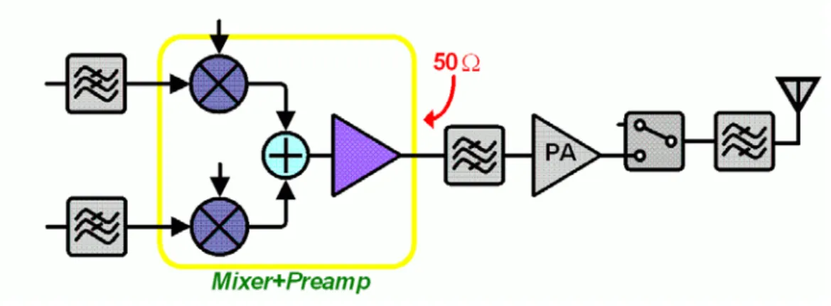
(17) existing designs with dual or multiple frequency bands [8], [9].The most popular architecture is to design individual transmitting paths for different communication standards. The disadvantage of such design is its large area required, and duplicated power consumption. And the more advanced design is to merge different modules (ex: LNA and mixer) to save current dissipation [1], or to design a single module with dual-band operation [2], which has saved the chip area and obtain higher integration level. In this thesis, the objective is to derive a transmitter design applied for dual-band dual-mode WLAN IEEE 802.11 a/b/g standard. The transmitter consists of a quadrature mixer and a power amplifier driver: pre-amplifier. The mixer has two input signals: base band modulated signal and local oscillator (LO) signal which provides the carrier frequency of up-conversion, and one output signal: radio frequency (RF) after up-conversion. Since the LO matching is not so critical, although operating on high frequency band, a novel mixer reuse structure with dual-band LO matching was proposed. After up-conversion by the mixer, the output signal of 5 GHz and 2.4 GHz then pass through a dual-band LC-tank filter which separates into two paths for further processing by two pre-amplifiers. The proposed RF front-end not only maintains its high-integration, it is also expandable to multiple frequency bands if necessary. These are the factors that make our RF. 2.
(18) front-end architecture highly suitable for the mobile systems in the future.. 1.3 Existing Architectures Based on the reason of easily integrating, the direct-conversion architecture was chosen rather than super-heterodyne architecture. Detail comparison will be described latter. The mixer design of the transmitter faces many compromises between conversion gain, local oscillator power, linearity, noise figure, port-to-port isolation, voltage scaling and power consumption, especially for 5 GHz than 2.4 GHz band design. TABLE 1 lists the literatures proposed in recent years. TABLE 1 5-GHz Transmitter Performance of Recently Literatures. JSSC[3] JSSC[4] 2000(a) 2002(a) Process. 0.25. 0.25. 2003(a). 2003(a). 0.18. 0.18. 0.18. 6. 5. -2.5. 2003(a) 2004(a/b/g) 2004(a/b/g). 15. OIP3(dBm) Carrier. ISSCC[8] ISSCC[9]. 0.18. 0.25. 19. P1dB(dBm) O-P1dB(dBm). JSSC[5] JSSC[6] JSSC[7]. 22.4. 29. 41. 38. 33.4. 51. 54. 50. -33. -29.3. 17.3/13.3. Suppression(dB) Side-band. 45. Rejection(dB) -33. EVM(dB) Output. 22. -5. 0/-1. 8//9. 134. 670/710. Power(dBm) TX Power. 120. 790. 380. 302. 135. PA LPF/VGA/PA DAC/LPF. LPF. Dissipation(mW) Integration. PA. And Fig. 1 summarize the required performance for each specification such as. 3.
(19) ouput-P1dB, OIP3, carrier rejection, side-band rejection and maximum output power, etc.. 60. 33~54. 50. J2000(a). 22~41. J2002(a). 40. J2003(a). 30 J2003(a). 13~17. 20. J2003(a). -2.5~6. 10. -5~0. I2004(a) I2004(b). m ) dB. ow er (. n( dB. R. O. an d. Si de -B. I2004(a/b/g). ut pu tP. ej ec. tio. ct io n ej e R. ar rie r C. ). (d B). Bm ) 3( d. O IP. B. (d Bm. m ) (d B dB. P1. O -P 1d. es s Pr oc. -10. ). 0. Fig. 1 Performance Summary of the Literatures. In this work, two 5 GHz CMOS direct-conversion transmitters with different circuit architectures have been implemented for 802.11a transmission specification. After comparing the performance of both architectures, one of the two implementations has been applied for another dual-band design. A novel mixer reuse dual-band transmitter has been implemented that is capable of operating at two different frequencies and satisfies the specification of 802.11a and 802.11b, respectively.. 4.
(20) 1.4 Organization This thesis describes the design of RF transmitter frond-end for 5 GHz and 2.4 GHz wireless LAN applications. Chapter 2 reviews two conventional transmitter architectures, and states the advantages and drawbacks of each architecture and also expresses why a direct-conversion architecture was chosen, what issues will induce and how to resolve. Chapter 3 introduces the IEEE 802.11a and 802.11b standard for transmission, and institutes the transmitter specification which could meet these two standards simultaneously. Chapter 4 deals with the analyses for mixer, and pre-amplifier, respectively. Chapter 5 then describes two implementations of 5 GHz transmitter. One is designed for high linearity while the other is designed for low power application. After comparing the performance of these two transmitters, a dual-band transmitter has been proposed. Chapter 6 shows the experimental results including layout considerations, high frequency balun design, testing setup, and measurement results. Chapter 7 draws a conclusion and states how to improve this work in the future.. 5.
(21) Chapter 2 Architecture. The recent surge in application of radio-frequency (RF) transceivers has been accompanied with aggressive goals: low cost, low power dissipation, and small form factor. The architecture and frequency plan of the RF transceiver play an important role in the complexity and performance of the overall system. Because the base band signal is produced in the transmitter and hence is sufficiently strong. There are fewer transmitter architectures than those of receivers, due to issues such as noise, interference rejection, and band selectivity being more relaxed in transmitter designs. Two of the most common choices in transceiver architecture are the traditional “super-heterodyne” and “direct conversion” architecture [11].. 2.1 2.1.1. Super-Heterodyne Transmitter Operation of Super-Heterodyne Transmitter. A transmitter architecture as shown in Fig. 2 is called “super-heterodyne” architecture [10]. In the first stage, after passing through the DAC and low-pass. 6.
(22) filter (LPF) to select the desired band signal, the base band modulated in-phase and quadrature-phase signals first up-converse to intermediate frequency (IF) by LO1, and then sum up. This stage is followed by a band-pass filter (BPF) to filter out-of-band image occurred from the mixer in the first stage. Continuously, the intermediate frequency signal up-converses again to expected RF band by LO2 and followed by another band-pass filter (BPF) to further filter out-of-band image and then a power amplifier driver and finally a power amplifier to amplify the signal to desired power level.. Fig. 2 Super-Heterodyne Transmitter. 2.1.2. Advantages and Drawbacks. Due to the twice of up-conversions, a super-heterodyne transmitter is also called “two-step transmitter”. By properly choosing the IF frequency, the frequency of two VCOs: LO1 and LO2 will be far from the frequency of the PA and this will prevent the “injection pulling” problem. The injection pulling phenomenon will be express later. Besides, since the in-phase and quadrature-phase signals are summed. 7.
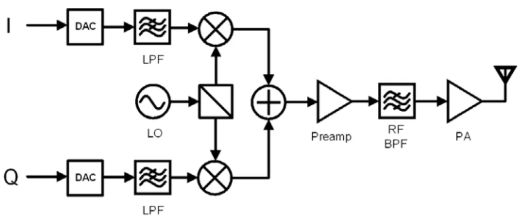
(23) at IF frequency which will be lower than RF frequency, I/Q mismatch problem resulted from process variation will be mitigated. However, a high-Q filter is required for the image-reject BPF, but a high-Q filter is hard to implement on chip. This violates the objectives of highly integration and low cost. In the meanwhile, two frequency synthesizers are needed for each LO1 and LO2 resulting in more circuits and higher power consumption. Finally, the frequency planning is complicated for LO1 and LO2 to avoid the image problem as far as possible.. 2.2 Direct-Conversion Transmitter 2.2.1. Operation of Direct-Conversion Transmitter. Another conventional architecture for transmitter is shown as Fig. 3. As implied by the name of “direct-conversion”, the base band in-phase and quadrature-phase signals first pass through the DAC and low-pass filter (LPF) and then directly up-converse to RF band by only one mixer and of course only one LO signal is required. After summing the I/Q signals on RF band, continuously, the signal passes through a power amplifier driver: pre-amplifier and a BPF as well, and finally passes through a power amplifier to provide enough power level to the antenna. As for the BPF, its function is the same as the last one in super-heterodyne transmitter to filter out-of-band image. 8.
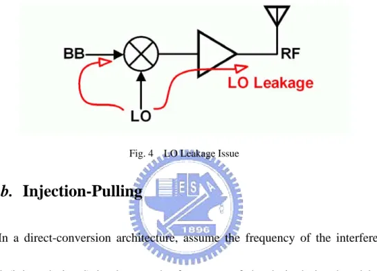
(24) Fig. 3 Direct-Conversion Transmitter. 2.2.2. Advantages and Drawbacks. Obviously,. the. difference. of. direct-conversion. transmitter. from. super-heterodyne one is that only one frequency synthesizer for LO is needed and no high-Q BPF is required. Therefore, comparatively speaking, a direct-conversion transmitter has the benefit of lower power consumption and highly integration. However, at the cost of suffering from some issues: LO leakage, injection-pulling, etc.. a. LO Leakage As we know that the coupling between radio frequency signals is very serious and almost inevitable. As for direct-conversion transmitter, the coupling effect will result in LO signal leaks to base band or to RF band as shown in Fig. 4. The LO leakage to base band will have LO signal modulated by itself. This “self-mixing” effect will induce a DC-offset term at the mixer output, and probably saturates the 9.
(25) DC operation of the next stage [12]. Besides, the LO leakage to RF band will desensitize next stage since for direct-conversion transmitter, the LO frequency is the same or almost close to the desired RF frequency. However, this issue will be mitigated by properly choosing the mixer architecture and carefully layout.. Fig. 4 LO Leakage Issue. b. Injection-Pulling In a direct-conversion architecture, assume the frequency of the interference signal (injected signal) is close to the frequency of the desired signal and has a magnitude comparable to the desired signal. When magnitude of the interference increases, frequency of the desired signal may shift toward the interference frequency and eventually be locked to that frequency. This phenomenon is called “Injection Pulling” or “Injection Locking” [11]. Fig. 5 describes the phenomenon of injection pulling that the LO pulling goes more critical as the output power rises. Because the carrier frequency is equal to the local oscillator frequency in a direct-conversion architecture and the power of a PA is higher than that of the local. 10.
(26) oscillator, it is easier to induce large interference. Even the injection level is 40 dB below original LO, it may still creates considerable disturbance. Thus, good isolation from PA to VCO becomes important. Usually, VCO must be followed by a buffer stage to improve isolation and driving ability.. Fig. 5 Injection Pulling [11]. Further, this phenomenon can be resolved by “offsetting” the LO frequency. That is, by adding or subtracting the output frequency of another oscillator. But another mixer and BPF are required. Additionally, a new architecture of “Even-Harmonic mixer” has been induced against this problem [13][14]. This novel architecture is able to merely use half of LO frequency to achieve the same RF modulated frequency.. 2.3 Summary The direct-conversion architecture is more easily to be integrated than super-heterodyne since the latter requires a high-Q band pass filter. Therefore large lump components are forced to be implemented off chip. The use of direct-conversion techniques is a promising approach for highly integrated wireless 11.
(27) transceivers due to their potential for low-power fully monolithic operation and extremely broad bandwidth. Their potential for broadband operation is especially important for future wireless communication applications, where a combination of digital cellular, GPS, and WLAN applications are required in a single portable device. Based on these reasons, the direct-conversion architecture is chosen as the system architecture.. 12.
(28) Chapter 3 System Behavior Analysis. In this chapter, the IEEE 802.11a and 802.11b standard will be introduced. Since IEEE 802.11g adopts both the modulations of 802.11a/b standard, a specification of transmitter front-end suited for 802.11 a/b/g will be instituted.. 3.1 3.1.1. Specification Introductions IEEE 802.11a Standard. a. Operating Channels The operating channel scheme for 802.11a standard is depicted in Fig. 6, which shall be used with the FCC U-NII (Unlicensed National Information Infrastructure) frequency allocation [15]. The total bandwidth is 300 MHz divided for lower, middle, and upper sub-bands. The lower and middle U-NII sub-bands accommodate eight channels in a total bandwidth of 200 MHz. The upper U-NII band accommodates four channels in a 100 MHz bandwidth. The centers of the outermost channels shall be at a distance of 30 MHz from the edge of band for the lower and 13.
(29) middle U-NII bands, and 20 MHz for the upper U-NII band. The total frequency range is 5.15-5.25 GHz for lower band, 5.25-5.35 GHz for middle band, and 5.725-5.825 GHz for upper band, respectively. The bandwidth of each channel is 20 MHz, and each channel has 52 sub-carriers for OFDM modulation with each sub-carrier having bandwidth of 300 kHz. The maximum output power constraint with antenna gain is 40mW for lower band, 200mW for middle band, and 800mW for upper band, respectively.. Fig. 6. Channel Allocation of 802.11a Standard. b. Transmit Spectrum Mask The transmitted spectrum shall have a 0dBr (dB relative to the maximum spectral density of the signal) of bandwidth not exceeding 18 MHz, -20dBr at 11Mhz frequency offset, -28dBr at 200 MHz frequency offset and -40dBr at 30 MHz frequency offset and above. The transmitted spectral density of the transmitted signal shall fall within the spectral mask, as shown in Fig. 7.. 14.
(30) Fig. 7 802.11a Transmit Spectrum Mask. c. PAPR Requirement As for PAPR constraints, since each channel in IEEE 802.11a standard composes of 52 sub-carriers. By imaging that each of the 52 sub-carriers of the OFDM signal is a single-tone sinusoid wave such that the composite waveform in the time domain will have large peaks and valleys. If the peaks of all 52 sinusoid waves should line up in time, the peak voltage will be 52 times larger than that of a single sinusoid wave. In this critical case, the peak-to-average ratio will be 10log (52)=17 dB. Therefore, the transceiver must be able to accommodate signals whose peak amplitudes are 17 dB larger than the average signal. This translates into the need for a large power back-off in the transmitter. However, in practical applications, since the signal peaks are infrequent, the peak-to-average ratio requirement can be significantly less than 17 dB without major degradation in the overall SNR. For instance, in the case of 16-QAM modulation, simulation indicates that a 6dB peak-to-average ratio degrades the system SNR by only 0.25 dB [4]. And in practice,. 15.
(31) peak-to-average ratios as low as 4 dB may meet the error vector magnitude (EVM) and packet error rate (PER) requirements of the IEEE 802.11a specifications. Generally, a 6dB PAPR is demanded for moderate performance. But in this thesis, the PAPR was set to be 7dB for 1dB design margin.. d. Center Frequency Leakage Certain transmitter implementations may cause leakage of the center frequency component. Such leakage shall not exceed -15 dB relative to overall transmitted power or, equivalently, +2 dB relative to the average energy of the rest of the sub-carriers.. 3.1.2. IEEE 802.11b Standard. a. Operating Channels The IEEE 802.11b standard can be discriminated by two operation areas: North American and European [16]. In this thesis, the design target is the North American operation. The operating channels scheme for 802.11b standard is shown as Fig. 8. The frequency range is from 2400 MHz to 2483.5 MHz with total bandwidth of 83.5 MHz. For non-overlapping operation, three channels are used and the channel center frequencies are: 2412 MHz, 2437 MHz, and 2462 MHz, respectively. Each channel has bandwidth of 20 MHz. As for overlapping operation, six channels are selected. The center frequency of each channel shall be at a distance of 10 MHz from the 16.
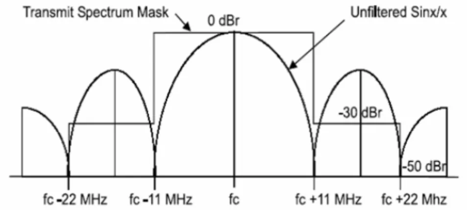
(32) others from 2412 MHz to 2462 MHz. The maximum allowable output power for North American operation is 1000mW.. Fig. 8. Channel Allocation of 802.11b Standard. b. Transmit Spectrum Mask The transmitted spectrum shall have a 0dBr (dB relative to the SIN(x)/x peak) bandwidth not exceeding 22 MHz, -30dBr at frequency offset of 11MHz to 22 MHz, -50dBr at frequency offset of 22 MHz and above. The transmitted spectral density of the transmitted signal shall fall within the spectral mask, as shown in Fig. 9.. Fig. 9 802.11b Transmit Spectrum Mask. 17.
(33) c. Center Frequency Leakage The RF carrier suppression, measured at the channel center frequency, shall be at least 15 dB below the peak SIN(x)/x power spectrum. And this RF carrier suppression shall be measured while transmitting a repetitive 01 data sequence with the scrambler disabled using D-QPSK modulation.. 3.1.3. Summary. As we know that the 802.11g standard adopts both the modulations of 802.11a and 802.11b with data rate from 1 to 54Mbps and the transmission requirement for 802.11g also agrees with 802.11a/b respectively. A simple summary of specification about 802.11 a/b/g is listed at TABLE 2. TABLE 2 802.11a/b/g Specification Summary. 802.11a/g Frequency range. 802.11b/g. 5.15~5.825 GHz 2400~2483.5 MHz. Channel bandwidth. 20MHz. About 20MHz. Total bandwidth. 300 MHz. 83.5 MHz. Modulation. OFDM. CCK/DSSS. Data rate. 6~54 Mbps. 1~11 Mbps. Maximum output power 200 mW(Middle Band). 1000mW(USA). Carrier suppression. 15 dBc. PAPR requirement. 4~6dB at least. 15 dBc. From the table above, in order to conform with the 802.11a and 802.11b or even 802.11g standards, a minimum operation bandwidth of 300 MHz is required. As for the maximum output power level will be discuss later. 18.
(34) 3.2 System Architecture The whole direct-conversion transceiver is shown as Fig. 10. The analog RF transceiver consists of a transmitter, a receiver, and single frequency synthesizer. The transmitter front-end contains two quadrature mixers for I/Q channel respectively and a single pre-amplifier while the back-end includes a band-pass filter, and a power amplifier.. RX A/D. Synthesizer. D/A Inter -face. PA. TX. Fig. 10 Analog Transceiver Architecture. 3.3 Specification Analysis In this section, the gain and linearity link-budget will be described. For transmitter, since the input signals come from base band modulated signals which have enough power level, the noise figure issue will be omitted. The transmitter chain of each block is shown in Fig. 11. They are in sequence DAC, LPF, 19.
(35) Quadrature-Mixer,. Preamp,. BPF,. PA. (power. amplifier),. Switch. of. transmitting/receiving, and at last a channel-select BPF from right to left. And finally, the signals pass through a RF antenna for transmission.. Fig. 11. 3.3.1. Transmitter Architecture. 802.11a/g. The IEEE 802.11a/g contains three sub-bands, and each band has different output power requirement. In this thesis, the lower band and middle band are the objective for 5 GHz design. For middle band design, the maximum output power with antenna gain is. 200mW = 10*log(. 200mW ) = 23dBm . 1mW. Subtracting from antenna gain of 6 dB, transmitter front-end average output power is 23dBm − 6dB = 17 dBm .. For OFDM modulation, an additional constraint of PAPR is demanded for 7 dB with 1dB design margin. Therefore, the transmitter front-end peak output power is. 20.
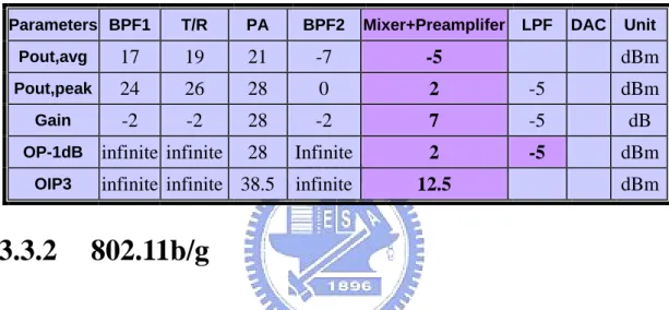
(36) 17 dBm + 7 dBm = 24dBm .. This value is required at the output of last BPF. A transmitter must be able to transmit this peak value rather be saturated. Therefore, the linearity of the transmitter front-end will be a “bottleneck” for our design. The system planning is shown as TABLE 3. The power amplifier gain was set to be 28 dB [10]. TABLE 3 802.11a/g System Planning Parameters BPF1. T/R. PA. BPF2. Mixer+Preamplifer. LPF. DAC. Unit. Pout,avg. 17. 19. 21. -7. -5. Pout,peak. 24. 26. 28. 0. 2. -5. dBm. Gain. -2. -2. 28. -2. 7. -5. dB. 28. Infinite. 2. -5. dBm. infinite. 12.5. OP-1dB OIP3. 3.3.2. infinite infinite. infinite infinite 38.5. dBm. dBm. 802.11b/g. As for IEEE 802.11b/g standard, for North American operation, the maximum output power is 1000mW 1000mW = 10 log( ) = 30dBm 1mW Subtracting from antenna gain of 6 dB: transmitter front-end average output power: 30dBm − 6dB = 24dBm. Similarly, this value is required at the output of last BPF. The system planning is shown at TABLE 4. If the power amplifier gain is also set to be 28 dB, a very interesting conclusion was arose that the specification of transmitter front-end for 802.11a and 802.11b are the same except the operation band. 21.
(37) TABLE 4 802.11b/g System Planning Parameters BPF1. T/R. PA. BPF2. Mixer+Preamplifer. LPF DAC. Unit. Pout. 24. 26. 28. 0. 2. -5. dBm. Gain. -2. -2. 28. -2. 7. -5. dB. 28. infinite. 2. -5. dBm. OP-1dB OIP3. infinite infinite. infinite infinite 38.5 infinite. 12.5. dBm. 3.3.3 Dual-Band Specification Summary Based on the results of system planning for 802.11a and 802.11b from TABLE 3 and TABLE 4, a dual-band transmitter front-end specification for 802.11 a/b/g. standard was specified at TABLE 5.. TABLE 5 Dual-Band TX-FE Specification. Parameters. 802.11a/b/g Specification. Frequency Range. 2.4-2.4835GHz/5.15- 5.825GHz. Conversion Gain. 7 dB. Input-P1dB. -5 dBm. Output P1dB. 2 dBm. OIP3. 12.5 dBm. RF Return Loss. <-15 dB. LO Return Loss. <-15 dB. Carrier suppression. <15 dBc. 22.
(38) Chapter 4 Circuit Analysis. Each system block in RF front-end will be discussed in detail in this chapter, including mixer and preamplifier circuit design and analysis. At first, the trade-off between gain and linearity will be described using model of cascaded nonlinearity stages. Then the design procedure and circuit analysis for mixer and preamplifier will be introduced.. 4.1 Transmitter Design Considerations A transmitter front-end system composes of a mixer and pre-amplifier. Since the signals are processed by these cascaded stages, it is important to know how the nonlinearity of each stage is refereed to the input of the cascade. In particular, it is desirable to calculate an overall input third intercept point in terms of the IP3 and gain of the individual stages. Consider two or more nonlinear stages in cascade as shown in Fig. 12 [10]. If the input-output characteristics of each stages are expressed, respectively, as. 23.
(39) y1 (t ) = α1 x(t ) + α 2 x 2 (t ) + α 3 x 3 (t ). (1). y2 (t ) = β1 y1 (t ) + β 2 y12 (t ) + β 3 y13 (t ). (2). the input third intercept point can be derived as. α12 α12 β12 1 1 ≈ 2 + 2 + 2 +… 2 AIP 3 AIP 3,1 AIP 3,2 AIP 3,3. (3). where AIP3,1 and AIP3,2 represent the input IP3 of the first and second stages and so on. Interestingly, proper choice of the values and signs of the terms can yield an arbitrarily high IP3. In practice, however, since the base band signal is produced in the transmitter and hence is sufficiently strong, the noise of the mixer is not so critical here as in receivers, other considerations such as noise, gain, and active device characteristics may not permit this choice. Besides, if each stage in a cascade architecture has its gain greater than unity, the nonlinearity of the latter stages becomes increasingly critical because the IP3 of each stage is effectively scaled down by total gain preceding that stage. This formula is merely an approximation, since each stage in a cascade has a narrow frequency band in RF systems. Thus, the nonlinearity terms which fall out of the band are heavily attenuated, and then are omitted. In practice, more precise calculations or simulations must be performed to predict the overall IP3.. 24.
(40) Fig. 12 Cascaded Nonlinearity Stages. 4.2 Mixer Design The main function for up-conversion mixers is to translate the BB frequency input signal into IF or RF band by multiplying LO frequency signal generated by local oscillator in the time domain. Multiplication thus results in output signals at the sum and difference frequencies of the input BB and LO signals. Theoretically, all devices with nonlinear characteristics can be mixers. The higher order terms of the characteristics offer the function of frequency translation.. 4.2.1. Mixer Topology. Mixers can be mainly discriminated by passive mixers and active mixers by their gain performance. Active mixer generally provides some gain but passive not. Further, for passive mixers, the widely used topology is passive switching mixer as shown in Fig. 13. This mixer has the benefits of high linearity, no DC power consumption and easier implementation, but at the cost of higher requirement of LO power which is hard to reach for local oscillator. Besides, isolation is always a weakness to passive mixer, resulting in LO leakage problem described in chapter 2.. 25.
(41) Fig. 13. Passive Mixer. For active mixers, two of the widely used topologies are single-balanced mixer and double-balanced mixer which are depicted in Fig. 14. Unlike passive mixers, these topologies would provide kind of gain and good isolation from LO to BB, although they would perform worse linearity, and power consumption. And most distinctness between single-balanced and double-balanced mixer is that the single-balanced mixer has still LO-RF feedthrough problem. This problem is more critical for direct-conversion architecture since the feedthrough term is located on desired RF band and would infringe the LO rejection constraint in both 802.11a/b specifications. Moreover, the double balance mixer has double conversion gain compared with the single balance mixer. So the double balance topology is chosen in our design. Detail analysis will be described in latter section.. 26.
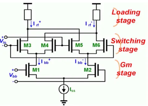
(42) (a). (b). Fig. 14 (a) Single Balanced Mixer (b) Double Balanced Mixer. 4.2.2. General Considerations. As shown in Fig. 15 is conventional double balance mixer which is also called “Gilbert cell” mixer. The operation can be divided into three stages: input gm-stage, switching-stage, and loading-stage. The gm-stage provides the transconductance that converts the input voltage into current domain. This stage also contributes most gain of an active mixer. Then, by switching the current signal in the switching-stage, nonlinearity effect will result in frequency translation. After the translation, current signals are again transformed to voltage domain by the loading-stage, and differentially output.. 27.
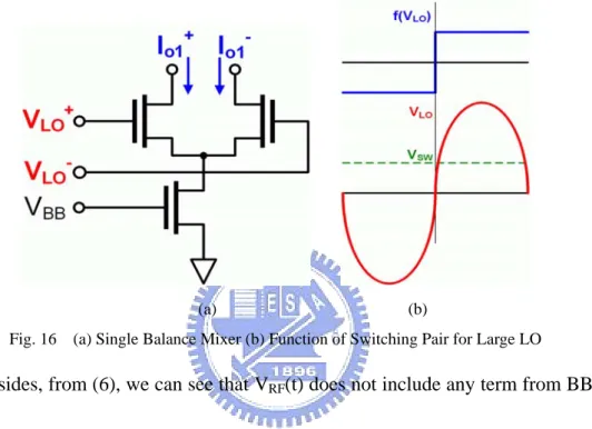
(43) Fig. 15 Gilbert Cell Mixer. 4.2.3. Conversion Gain. Since the switching level of the switching-stage in the mixer will enormously affect gain performance, here the analysis of conversion gain will be sorted by large and small LO amplitude [19].. a. For Large LO Amplitude The operation of the switching-stage is a nonlinear function of VLO expressed by f(VLO). If we assume BB and LO signal are both sinusoid waveform which are expressed as VLO (t ) = ALO cos ωLO t and VBB (t ) = ABB cos ωBB t . For assuming LO amplitude is large, f(VLO) can be modeled by using the sgn function with a periodic function oscillating at ωLO and which can be further expanded in a fourier series with fundamental frequency ωLO :. 28.
(44) nπ sin 1 ∞ 2 cos nω t f(VLO )= + ∑ LO π n 2 n =1 2. (4). as shown in Fig. 16. Therefore, we can derive the RF output signal is + − + − (t ) − VRF (t ) , and in which VRF VRF (t ) = VRF (t ) and VRF (t ) are the positive and. negative port of the differential output. Furthermore, ⎧ 2 ⎫ ⎡1 2 ⎤ ⎪ ABB cos BB t ⋅ g m ⋅ ⎢ 2 − π cos ωLO t + 3π cos 3ωLO t − …⎥ ⎪ ⎪ ⎣ ⎦ ⎪ + VRF (t ) = ⎨ ⎬ ⋅ RL 1 2 2 ⎡ ⎤ ⎪ +(−1) ⋅ A cos t ⋅ g ⋅ + cos ω t − cos 3ωLO t + …⎥ ⎪ BB BB m ⎢ LO ⎪⎩ 3π ⎣2 π ⎦ ⎪⎭ nπ ⎛ ⎞ ⎜ ∞ sin 2 ⎟ = (−1) ⋅ ABB cos BB t ⋅ g m ⋅ 2 ⎜ ∑ cos nωLO t ⎟ ⋅ RL nπ ⎜ n =1 ⎟ ⎝ ⎠ 2. (5). , and similarly, nπ ⎛ ⎞ ∞ sin ⎜ − 2 cos nω t ⎟ ⋅ R . VRF (t ) = ABB cos BB t ⋅ g m ⋅ 2 ⎜ ∑ LO ⎟ L nπ ⎜ n =1 ⎟ 2 ⎝ ⎠. So nπ ⎛ ⎞ ∞ sin ⎜ + − 2 cos nω t ⎟ ⋅ R VRF (t ) = VRF (t ) − VRF (t )=(−1) ⋅ ABB cos BB t ⋅ g m ⋅ 4 ⎜ ∑ LO ⎟ L nπ ⎜ n =1 ⎟ ⎝ ⎠ 2. (6). , and then with trigonometric expansion, this term further becomes VRF (t ) = (−1) ABB g m 4 RL. 1. π. [cos(ωBB + ωLO ) + cos(ωBB − ωLO )]. (7). of the fundamental term. For the upper side band mixing, after dividing by VBB (t ) , we get the conversion gain of. 29.
(45) Gc =. 4. π. g m RL. (8). From (8) that in order to achieve high conversion gain, the only way is to increase the transconductance of the gm-stage and loading RL. Furthermore, one thing important appears that Gc is independent of ALO.. (a). (b). Fig. 16 (a) Single Balance Mixer (b) Function of Switching Pair for Large LO. Besides, from (6), we can see that VRF(t) does not include any term from BB or LO. Ideally, the LO-to-BB and LO-to-RF isolation is infinite for double balance mixer. But process variation will induce gain and phase mismatch around switch stage. Therefore, carefully layout and symmetry board design still dominate isolation performance.. b. For Small LO Amplitude Now, let us assume LO amplitude is small which is between V+ and V- and. f (VLO (t ) ) =. VLO − V− . V+ − V−. To simplify our discussion, let us for the present case set V+=1 and V-=0 as shown in 30.
(46) Fig. 17, and then f (VLO (t )) = VLO (t ) = ALO cos ωLO t . The derive of VRF+ (t ) is now easier which becomes ⎧⎪[ ABB cos BB t ⋅ g m ⋅ (-1) ⋅ ALO cos ωLO t ] ⎫⎪ VRF+ (t ) = ⎨ ⎬ ⋅ RL ⎪⎩+ [ (-1) ⋅ ABB cos BB t ⋅ g m ⋅ ALO cos ωLO t ]⎪⎭ = (−1) ⋅ ABB cos BB t ⋅ g m ⋅ 2 ⋅ ALO cos ωLO t ⋅ RL , and similarly, − VRF (t ) = ABB cos BB t ⋅ g m ⋅ 2 ⋅ ALO cos ωLO t ⋅ RL ,. + − VRF (t ) = VRF (t ) − VRF (t ) = (−1) ABB cos BB t ⋅ g m ⋅ 4 ⋅ ALO cos ωLO t ⋅ RL .. Now the equation can be expanded again into VRF (t ) = (−1) ABB ALO g m 2 RL [ cos(ωBB + ω LO ) + cos(ωBB − ωLO ) ]. (9). And the conversion gain is Gc = 2 ALO g m RL. (a). (10). (b). Fig. 17 (a) Single Balance Mixer (b) Function of Switching Pair for Small LO. Referring to (10), however, that Gc is proportional to ALO, which is not acceptable for our design. Since VLO (t ) is usually generated from some frequency synthesizer, 31.
(47) and its exact amplitude is hard to control, leading to a Gc that is hard to control. As a result, the switching-stage has been designed to operate at border between large and small LO amplitude. Operating at this border will gain a Gc independent of ALO with requiring less LO amplitude. As we know that, for a differential pair, the completely switching voltage is Vsw =. 2Is = 2Vov . ⎛W ⎞ µ Cox ⎜ ⎟ ⎝L⎠. (11). To decrease the requirement of LO amplitude of switching-stage, we must have over-drive voltage of switching-stage as small as possible [17]. And from (11), device ratio must be as large as possible leaving the trade-off between conversion gain and LO amplitude requirement by modulating Is value.. 4.2.4. Linearity. This section focuses on another important performance for transmitter, which is linearity. First, we assume the switching-stage operates at large enough LO amplitude and consequently do not contribute distortion. Therefore, distortion comes primarily from the input V-I conversion: gm-stage, and also assume that this distortion is dominated by nonlinear square law I-V characteristics of the MOS transistors biased in saturation. Referring to the source-couple pair (SCP) M1-2 in Fig. 15, from the square law. 32.
(48) [18], we know that I bb+ =. k W (Vgs1 − Vt ) 2 , k = µ0cox . L 2. (12). Since the source of the SCP is common node that Vbb+ − Vgs1 = Vbb− − Vgs2 => Vgs1 = Vbb+ − Vbb− + Vgs2 = Vbb + Vgs2 .. (13). Substituting (13) into (12), we obtain k (Vbb + Vgs2 − Vt ) 2 2. (14). k 2 I bb− (Vgs2 − Vt ) 2 => Vgs2 − Vt = 2 k. (15). I bb+ = Similarly, I bb− =. Again substituting (15) into (14), we get ⎛ 2 ( I SS − I bb+ ) ⎞ k⎜ + ⎟ . I bb = Vbb + ⎜ ⎟ 2 k ⎝ ⎠ 2. After normalizing by I. + bb n. (16). 2 I bb+ 2I = and I SS n = SS , (16) is changed to k k. ). (. I bb+ n = Vbb + I SS n − I bb+ n .. (17). That is. Vbb = I bb+ n − I SS n − I bb+ n =. I SS n 2. + ibb+ n −. I SS n 2. − ibb+ n ,. (18). where ibb+ n is the small signal part of I bb+ n . And then factoring out the I SS n , we get Vbb =. I SS n ⎛ 2ibb+ n 2ibb+ n ⎜ 1+ − 1− I SS n I SS n 2 ⎜ ⎝. ⎞ ⎟, ⎟ ⎠. (19). which (19) gives Vbb in terms of ibb+ n . The square root terms in (19) can be expanded. 33.
(49) around. 2ibb+ n I SS n. and we have. Vbb =. =. 2 3 ⎡ ⎤ ⎛ 2ibb+ ⎞ 1 ⎛ 2ibb+ ⎞ ⎛ 2ibb+ ⎞ 1 1 ⎢ (1 + ⎜ n ⎟ − ⎜ n ⎟ + ⎜ n ⎟ + …) ⎥ ⎥ 2 ⎜⎝ I SS n ⎟⎠ 8 ⎜⎝ I SS n ⎟⎠ 16 ⎜⎝ I SS n ⎟⎠ I SSn ⎢ ⎢ ⎥ 2 3 2 ⎢ + + + ⎥ ⎛ 2i ⎞ ⎛ 2i ⎞ ⎛ 2i ⎞ ⎢ −(1 − 1 ⎜ bbn ⎟ + 1 ⎜ bbn ⎟ + 1 ⎜ bbn ⎟ + …) ⎥ ⎢ ⎥ 2 ⎜⎝ I SS n ⎟⎠ 8 ⎜⎝ I SS n ⎟⎠ 16 ⎜⎝ I SS n ⎟⎠ ⎣ ⎦. (20). I SSn ⎡ 2ibb+ n 1 ⎛ 2ibb+ n ⎢ + ⎜ 2 ⎢ I SS n 8 ⎜⎝ I SS n ⎣. (21). 2 ⎤ ⎞ ⎥ … + ⎟ ⎟ ⎥ ⎠ ⎦. Since Vbb is input and ibb+ n is output, each ibb+ n term can also be expanded as a Taylor series in power of Vbb . That is ibb+ n = a1Vbb + a2Vbb2 + a3Vbb3 + …. (22). Substituting each ibb+ n term in (21) using (22), we have. Vbb =. ⎡ 2 ⎤ 2 3 ⎢ I ( a1Vbb + a2Vbb + a3Vbb + …) + ⎥ I SSn ⎢ SSn ⎥ 2 ⎢ ⎥ 2 ⎢1 ⎛ 2 ⎞ 2 2 3 ⎜ ⎟ a V + a2Vbb + a3Vbb + …) + …⎥ ⎢ 8 ⎜ I ⎟ ( 1 bb ⎥ ⎣⎢ ⎝ SS n ⎠ ⎦⎥. (23). Finally, we can solve for the coefficients a1 , a2 , a3 ,… by equating the coefficients of Vbb , Vbb2 ,… on both sides of (23). For the Vbb term, 1=. ⎞ I SS n ⎛ 2 a1 ⎟ => a1 = ⎜ 2 ⎜⎝ I SS n ⎟⎠. I SS n 2. .. (24). For the Vbb2 term, 0=. ⎞ I SS n ⎛ 2 a2 ⎟ => a2 = 0 . ⎜ 2 ⎜⎝ I SS n ⎟⎠ 34. (25).
(50) For the Vbb3 term, 0=. I SS n ⎛ 2 1⎛ 2 ⎜ a3 + ⎜ 2 ⎜ I SS n 8 ⎜⎝ I SS n ⎝. 3 ⎞ 3⎞ 1⎛ 2 ⎟ a1 ⎟ => a3 = − ⎜ ⎟ ⎟ 8 ⎜⎝ I SS n ⎠ ⎠. 2. ⎞ 3 ⎟ a1 . ⎟ ⎠. (26). 3 a3 2 Abb [10], then substituting by (24) and (26), we 4 a1 3 1 2 3 k 3 k 2 get IM 3 = Abb = Abb2 = Abb (27) 16 I SSn 16 2 I SS 32 I SS. And as we know that, IM 3 =. , for which k = µ0cox. W and (27) can be wrote as L IM 3 =. 3 32. µ Cox I SS. W1 L1. Abb2 .. (28). And then AIP2 3 =. 32 2 I D1 3 µ C W1 0 ox L1. (29). In order to mitigate the nonlinearity effect due to interferences, that is low IM 3 and high AIP3 are desired. Referring to (28) and (29), we observe that high Iss is unavoidable and ID1 as well, while the. W1 ratio must be kept low. But high Iss will L1. burn more power consumption, and low. W1 will decrease the main source of L1. conversion gain, leaving a trade-off between power consumption, linearity, and conversion gain to design a mixer. If Vbb is small, then the current flowing through M1 can be assumed to be equal to that through M2, or half of I SS . Then (29) can be rewrote as. 35.
(51) 1 W 2 µ0Cox 1 (VGS1 − Vt ) 2 32 2 I D1 32 2 32 L1 AIP2 3 = = = (VGS 1 − Vt ) 2 W 3 µ C W1 3 3 µ0Cox 1 0 ox L1 L1. (30). , and AIP3 = 4. 2 (VGS1 − Vt ) . 3. (31). From (31), we also see that, a high over-drive voltage (Vov) of the input gm-stage is desired to achieve higher linearity.. 4.3 Pre-amplifier design In the transmitter design, a power amplifier (PA) is followed by the up-conversion mixer to provide the required output power to a 50- Ω antenna. For most of Wireless LAN applications, a PA circuit must be able to achieve 25-30dBm output power. In order to deliver required output power to a 50- Ω antenna at lower supply voltages, a matching network can be interposed between the PA and the load. The matching network transforms RL to a smaller value such that the limited voltage swing provided by the PA can still deliver the required output power. The enormous currents in the output device and the matching network are one of the difficulties in the design of power amplifiers and especially the package. Besides, a series resistance of a few tens of milliohms in the transistor, and the “radio-frequency choke” (RFC), or the matching network may result in a considerable loss, therefore, a precise modeling of transistors or even package is indispensable for PA designer. 36.
(52) In practice, PA design has involved a substantial amount of trial and error, and an additional power supply voltage will be required to obtain the high power gain. Due to these reasons, a discrete and off-chip implementation of PA is chosen in our transmitter design. Instead, following the up-conversion mixer is a power amplifier driver (Pre-amplifier). This preamplifier stage will be design as the same way of designing a power amplifier, but the power gain constraint is released here. As described in chapter 3, an off-chip PA with power gain of 20~28dB is required for system specification, and the total gain of mixer with adding preamplifier stage is set to be 7~15dB [10].. 4.3.1 General Considerations Generally, in the field of communication, we can distinguish signals into two parts: amplitude and phase. As a result, power amplifier can also be divided into two categories: one is linear operation and another is constant-envelope operation [21]. The transistor in linear operation acts as a current source and the RF output power is proportional to the RF input power. The transistor “on” voltage does not saturate. Otherwise, the transistor in constant-envelope operation operates as a switch. The linear operation includes class-A,B,C,AB type power amplifier, and which is suitable for linear amplitude modulation, while the constant-envelope operation includes class-D,E,F type power amplifier, and which is suitable for phase 37.
(53) modulation. Roughly speaking, the linear operation has high linearity but poor efficiency. However, the constant-envelope operation has excellent efficiency. The need for linear power amplifiers arises in many RF applications, especially, for multi-carrier systems, for example, in this thesis, OFDM application in 802.11a/g standard. Since amplifiers simultaneously process many channels, it needs to be linear enough to avoid cross modulation. The nonlinearity of PAs is usually characterized by a two-tone test. For adjacent channel interference, the third-order IM components are important. At present, most linear PAs designed for portable devices employ a class A output stage and exhibit efficiencies around 30% to 40%.. 4.3.2. Loading Line Theorem. As we know that, a small signal amplifier adopts conjugate matching to obtain maximum output power as shown in Fig. 18, where RL=Ro. However, as signal power increases, the output power will be less than expected due to the limit of current or voltage driving capability.. Fig. 18 Output Impedance with Linear Resistance Model. Therefore, different from the design of small signal amplifier, a power 38.
(54) amplifier is biased at the middle of maximum output swing of current and voltage as shown in Fig. 19. Besides, by properly choosing Rload, the signal will have maximum swing under the limit of current and voltage. And the maximum output power is larger than that by conjugate matching.. Fig. 19 PA Bias Condition and Loading Line. We will introduce two extreme kinds of power amplifiers: class A and class B [20]. Class A has excellent linearity but poor efficiency, while class B has better efficiency but worse linearity.. a. Class A PA The bias point for class A PA is depicted in Fig. 19. At first, the optimum Rload is decided by Ropt =. Vmax − Vknee I max 39. (32).
(55) We have Vrms =. (Vmax − Vmin ) (I − I ) , I rms = max min 2 2 2 2. (33). and VDC =. (Vmax + Vmin ) (I + I ) , I DC = max min . 2 2. (34). The output power can be expressed as: Pout = Vrms I rms =. (Vmax − Vmin ) ( I max − I min ) (Vmax − Vmin )( I max − I min ) = 8 2 2 2 2. (35). The dc power consumption is also shown as: PDC = VDC I DC =. (Vmax + Vmin ) ( I max + I min ) (Vmax + Vmin )( I max + I min ) = 2 2 4. (36). From (35) and (36), and by definition that the drain efficiency of a class A PA is: (Vmax − Vmin )( I max − I min ) Pout 8 = ≤ 50% η= V + V ( )( PDC max min I max + I min ) 4. (37). Ideally, for Vmin=Imin=0, the efficiency of a class A PA is 50%. In fact, since the device’s characteristic such as breakdown voltage and knee voltage are not equal to 0, the efficiency is always less than 50%.. b. Class B PA As for class B PA, it conducts half a cycle, and the drain current is severely clipped which would induce serious nonlinearity and result in worse linearity than class A PA. The only difference from class A PA is dc current as:. 40.
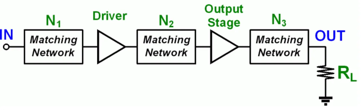
(56) I DC =. 1 2π. ∫. 2π. 0. I max sin θ dθ =. I max. π. .. (38). And the dc power consumption is expressed as: PDC = VDC I DC =. (Vmax + Vmin ) I max I max (Vmax + Vmin ) = . 2 2π π. (39). The drain efficiency of a class B PA is. η=. Pout π (Vmax − Vmin ) π = < ≈ 0.785 . PDC 4 (Vmax + Vmin ) 4. (40). It can be seen from (40) that class B PA has a maximum efficiency of around 78 percent which is superior to class A PA.. 4.3.3. Two-Stage Configuration. Most power amplifiers employ a two-stage configuration, with matching networks placed at the input, between the two stages, and at the output as shown in Fig. 20. Since the output stage typically exhibits a power gain of less than 10 dB, a high-gain driver is added so as to lower the minimum required input level. The input and output matching networks in Fig. 20 serve different purposes: N1 provides a 50- Ω input impedance, while N3 amplifies the voltage swings produced by the output stage so as to deliver the required power to RL. In our transmitter system, since the up-conversion mixer and preamplifier are implemented on a single chip, the first matching network for 50- Ω input matching can be removed. As for N2, it provides desired load and source impedance simultaneously for driver stage and output stage and hence simplifies the design procedure. 41.
(57) Fig. 20. Two Stage Configuration. 42.
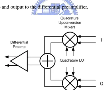
(58) Chapter 5 Circuit Implementation. According to the specification expressed in TABLE 5, a mixer must perform high 1dB compression point. As we know that I/V transfer characteristic of the gm-stage dominates the linearity of a mixer. There are several circuit techniques for improving the linearity of MOS transconductance elements. In this chapter, two 5GHz transmitter front-end utilizing two of the techniques will be introduced and implemented. One is to degenerate the source-coupled pair by a MOS transistor operating in the triode region [22] which is designed for higher linearity, whereas another is to simply add two auxiliary cross-coupled differential pairs to the source-coupled pair [23], [24], meanwhile, with the on-chip differential-to-single circuit, this transmitter front-end has better power consumption and is designed for low power application. And finally, a novel structure of mixer-reuse dual-band transmitter front-end will be proposed. Simulation results also have been listed after each circuit.. 43.
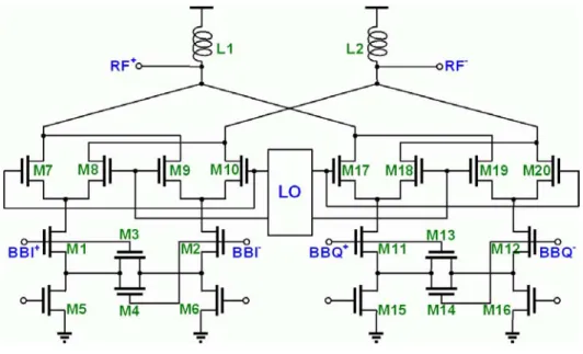
(59) 5.1 5GHz TX-FE for High Linearity Design The differential topology is employed throughout this transmitter front-end circuit to minimize the undesired coupling, especially the local oscillator leakage though the mixers to the antenna as it causes the dc offset to corrupt the desired low-frequency signals at receiver. The circuit block is depicted in Fig. 21. The direct-conversion architecture was adopted. Two mixers were employed to up-converse the base band I/Q signals respectively with quadrature local oscillator signals. The RF quadrature signals are then summed up and output to the differential preamplifier.. Fig. 21 5GHz TXFE for High Linearity Circuit Block. 5.1.1 Mixer Design Fig. 22 is the illustration of the first linearization technique. Transistors M1 and M1’ form the input differential pair while M3 and M3’ provide the bias current, and the transfer characteristic of which is linearized by the voltage-controlled 44.
(60) degeneration “resistors” M2 and M2’.. Fig. 22 Gm-stage using Triode-Region MOS Degeneration. In order to get a qualitative understanding of the behavior of this new input stage, the circuit is first analyzed using the simple square-law MOSFET. For convenience, the following parameters are introduced [25]:. β1 4β 2. (41). ∂I out I bias |@Vin =0 = ∂Vin a(VGS − VT ) M 1. (42). a = 1+ and gm0 = where β = µ 0 cox. W . For low values of the input voltage Vin, transistors M2 and L. M2’ are operated in triode region and we can get another normalized transfer characteristic as followed: i = v 1− , where v = g m 0. v2 4. (43). Vin I and i = out . An interesting conclusion comes out that within I bias I bias. a limited input voltage range the transfer characteristic of the input gm-stage is similar to that of a conventional source-coupled pair which is biased at an overdrive voltage of a(VGS − VT ) M 1 . However, when the swing of input signal voltage 45.
(61) increases, M2’ would eventually enter the saturation region, whereas M2 stays in the triode region because VGS,M2 is increasing but VGS,M2’ is decreasing. In this way, the equivalent degeneration resistance may not have distinct change, and the gm characteristic would maintain constant for wider input range. The simulation result of gm transfer characteristic is shown in Fig. 23 and the ripple in the gm curve can be reduced by lowering the quiescent gate overdrive voltage VGS-VT of the. Gm1. transistors.. 0.011 0.010 0.009 0.008 0.007 0.006 0.005 0.004 0.003 0.002 0.001 0.000. m9. m9 indep(m9)=0.114 Gm1=0.008 -0.6. -0.4. -0.2. 0.0. 0.2. 0.4. 0.6. indep(Gm1). Fig. 23 Gm-stage Transfer Characteristic. If the input common-mode voltage is not constant with respect to the bulk potential, even-order terms will appear in the v/i transfer characteristic. These distortions may be minimized by increasing the bulk reverse voltage to reduce the body effect. Furthermore, for a purely differential mode input signal, the remaining even-order distortions would result from device mismatch, which has to be minimized by appropriate layout disposition. Besides, for transistors operating more. 46.
(62) deeply in strong inversion, the optimum ratio β1 / β 2 is slightly larger than 6. On the contrary, that “hump” tends to disappear at lower current densities where the optimum β1 / β 2 is smaller than 6. When the ratio β1 / β 2 has been decided, referring to (29), in order to achieve high IP3, the bias current ID must be large and input dimension ratio must be small. But high gain requires high transconductance indicating high ID and W/L is desired which leaves a compromise between transconductance and linearity. The I/Q quadrature Gilbert-type mixer is depicted in Fig. 24. The loading resistors have been replaced by inductors due to the finite voltage headroom issue. The inductors were designed to resonate the capacitance seen from output nodes of the mixer at frequency of 5.25GHz by f =. 1 2π LC. .. (44). A conjugate matching at the output loading will transfer the maximum output power to the next stage. No doubt that parasitic capacitance of the input of next stage will be taken into consideration in the simulation. Referring to the discussion in section 4.2.3, in order to perform more ideal switch feature, and achieve higher linearity and high conversion gain and also mitigate the requirement of LO amplitude, the switching-stage is designed to have as less as possible Vov. From (11), the W/L of the switching-stage is required to be. 47.
(63) large, and Is is to be small. But large size of the transistor will induce considerable parasitic capacitance at the common drain of the switching-stage, which are either output nodes of mixer. The large capacitive characteristic would force to lower the loading inductance for output resonance. The loading impedance Z load = Qω L thus drops and then the gain of mixer drops in the same manner. Hence, leaving an optimum size of switching-stage for specified LO amplitude and bias current.. Fig. 24 Quadrature Gilbert-Type Mixer. 5.1.2 Preamplifier Design The differential outputs RF+ and RF- of the mixer then couple to the preamplifier with two series ac couple capacitors. In this way, the DC offset issue comes from self-mixing of mixer can be eliminated. The preamplifier employs two-stage configuration we described before, and of course, adopts fully-differential topology. The circuit is depicted in Fig. 25. The first stage is a common-source. 48.
數據
+7
相關文件
The results contain the conditions of a perfect conversion, the best strategy for converting 2D into prisms or pyramids under the best or worth circumstance, and a strategy
(A)憑證被廣播到所有廣域網路的路由器中(B)未採用 Frame Relay 將無法建立 WAN
✓learning contextualized word embeddings specifically for spoken language. ✓achieves better performance on spoken language
This design the quadrature voltage-controlled oscillator and measure center frequency, output power, phase noise and output waveform, these four parameters. In four parameters
Results indicate that the proposed scheme reduces the development cost, numbers of design change, and project schedule of the products, and consequently improve the efficiency of
The main objective of this system is to design a virtual reality learning system for operation practice of total station instrument, and to make learning this skill easier.. Students
The results obtained of this study include that (1) establishment of windows programming for the tunnel wriggle survey method, (2) establishment of windows
Hoping that the results of this study can provide suggestions for educational authorities and supplement schools to elevate the quality of elementary supplement schools.. The
