國立交通大學
電子工程學系 電子研究所碩士班
碩 士 論 文
奈米碳管記憶體之電荷儲存效應研究
A Study on the Charge Storage Effect of
Carbon Nanotube Memory
研
究
生:王俊凱
指 導 教 授:崔秉鉞 教授
奈米碳管記憶體之電荷儲存效應研究
A Study on the Charge Storage Effect of
Carbon Nanotube Memory
研究生:王俊凱 Student
:
Chun-Kai
Wang
指導教授:崔秉鉞 Advisor
:
Bing-Yue
Tsui
國立交通大學
電子工程學系 電子研究所
碩士論文
A thesis
Submitted to Department of Electronics Engineering & Institute of Electronics
College of Electrical Engineering and Computer Science
National Chiao Tung University
in Partial Fulfillment of the Requirement
for the Degree of Master
in
Electronic Engineering
2009
奈米碳管記憶體之電荷儲存效應研究
研究生:王俊凱
指導教授:崔秉鉞
國立交通大學電子工程系 電子研究所碩士班
摘要
本論文研究奈米碳管在電場下的電荷儲存效應,並將此概念實際應用在現有的記憶 體元件上。元件的電性量測、材料分析以及數值模擬的結果都將會在論文中被探討。 本論文中的記憶體元件是採用一基本的金氧半場效電晶體結構。利用旋塗法將碳管 溶液均勻地散佈在晶片表面。奈米碳管以介電層包覆,形成電荷儲存層。掃描式電子顯 微鏡的觀察結果發現,奈米碳管在氧化鋁表面的散佈情況極佳,大幅改善旋塗製程在氧 化矽表面的碳管分布不均問題。碳管散佈在這兩種表面都被實際做成元件以探討其電 性。沒有碳管塗佈的元件對照組則沒有表現出任何的記憶特性。 掃描式電容顯微鏡在本論文中被用來對介電層底下的奈米碳管作更進一步的分 析。有埋藏碳管的區域與沒有碳管的區域表現出截然不同的掃描電容訊號。利用金屬探 針在介電質表面施加電壓並且觀察隨時間變化的掃描電容二維圖形,更進一步的確認奈 米碳管就是造成電荷儲存效應的原因,並且發現電荷是以局部而非整根碳管的方式儲 存。這表示,造成記憶效應的的電荷改變是較局部性的機制所造成,而不是儲存在碳管 中的自由載子。 另外,本論文亦利用元件模擬軟體,討論通道上方帶電的單根奈米碳管其產生的電 場對元件電性有何影響。結果發現,如果此帶電區域平行於通道方向,則對於 N 型場效 電晶體而言,正電荷儲存會很容易造成電性上的變化:一條狹窄的正電帶即可提前導通 其下方的通道,並產生可觀的導通電流;如果是負電荷儲存在此狹窄的帶電區域,則其 對通道的調變效果將很難被觀察到。反之,如果帶電區域垂直於通道方向,則負電造成的能障將會對通道產生調變,而正電則無法造成影響。
雖然碳管記憶體初步的電性量測結果無法達到目前量產的記憶體元件之水準,但隨 著元件尺寸的持續微縮,現今的電荷儲存材料也將會面臨到許多製程上的問題,而奈米 碳管擁有一些獨特的優勢,在未來或許能成為解決的方案之一。另一方面,隨著掃瞄探 針技術越來越成熟,在未來也必定能對碳管元件做出更多更加深入的分析。
A Study on the Charge Storage Effect of
Carbon Nanotube Memory
Student: Chun-Kai Wang
Advisor: Bing-Yue Tsui
Department of Electronics Engineering
Institute of Electronics
National Chiao Tung University
Abstract
This thesis studies the electrical field-induced charge storage effect of carbon nanotubes (CNTs). The storage property is further applied in practical memory device implementation. Electrical characterization, material analysis, and computer modulation of the devices will all be discussed.
Memory device in this thesis took a typical metal-oxide-semiconductor field effect transistor (MOSFET) structure. By spin-coating method, carbon nanotubes were uniformly spread onto wafer surface. Nanotubes were covered by dielectric materials and become a trapping layer. Scanning electron microscopy (SEM) images show that carbon nanotubes have well dispersion quality on Al2O3 surface. This property substantially solves the segregation
and uneven distribution problems of coating nanotubes on SiO2 surface. CNTs coated on these
two surfaces were both made into devices. Control sample without carbon nanotube coating were also prepared and verified. In that case, no memory effect was observed.
nanotubes under dielectric layer. Completely different SCM signals were observed from the regions with and without nanotube underneath. By scanning again and again, a time-variant image was obtained and more details of the charging effect were revealed. First, the carbon nanotube was proved to be the essential reason for the memory effect. Moreover, the charging effect appeared locally on nanotubes instead of a whole-tube phenomenon. That also means charges are stored in the local sites around the nanotubes, not as free carriers in CNTs.
Numerical simulation works in this thesis discussed the situation of a single charged nanotube parallel or perpendicular to the channel (source to drain) direction, and to determine the channel modulation under these conditions. The results show that if the charged region is parallel to channel, positive charges would have strong effect on nMOSFET’s characteristics. A narrow line of positive charge can turn on the channel beneath it and causes a considerable on-current. But if the tube is negatively charged, its modulation effect would be hard to detect. On the other hand, if the tube is perpendicular to the channel, negative charges would easily modulate electrical characteristics while positive charges cannot.
Although the preliminary results of carbon nanotube memory cannot compete with commercial memory devices today, the study is not worthless. As the device continuously scaled down, many charge storage materials used in today’s memory device would confront some problems. Carbon nanotubes, with some unique advantages, might become one of the solutions in the future. Furthermore, as scanning probe techniques evolve, more detail analyses of nanotube devices could be done.
誌謝
這一年多在交大的研究生生活,我受到身邊許許多多人的幫助,無論是在研究上或 生活上。因為你們的協助,讓我得以順利的完成碩士學業。謹以此文致上最由衷的感謝。 首先要感謝我的指導教授,崔秉鉞老師。大學時便在老師的親自指導之下進行專題 研究,直到如今即將從老師的團隊中畢業,老師在我做學問的這條路上一直指引著方 向。在學術上決不妥協的態度,以及對學生不遺餘力的付出,讓我受到很深的影響。 在實驗上,感謝國家奈米元件實驗室與交大奈米中心提供的製程機台,以及交大電 子研究所計測實驗室提供的電性量測機台。要特別感謝的是 NDL 奈米元件材料分析組的 周棟煥、林宏旻兩位工程師。在棟煥的全力支持與幫忙之下,才能得到寶貴的 SCM 掃描 結果,真的很感謝你。也非常感謝儀器科技研究中心的志忠、孟諺、智傑、文浩、柏亨, 在原子層沉積製程上的幫助,以及在儀器預約上的幫忙,讓我能夠順利的進行我所需要 的實驗。 而在日常生活中,相處最久的就是實驗室的夥伴們了。回顧這些日子,我很慶幸自 己當初加入了這個和樂融融的大家庭。沒有夥伴們在實驗上的幫忙與學術上的討論,我 的研究不可能完成。感謝振銘學長帶領我學習無塵室中大多數的機台,也幫忙我進行了 諸如曝光、FIB-SEM 等無法自行操作的步驟,讓我的實驗進度大幅超前;感謝季霈學長 在學術問題上給予寶貴的建議與指導;志民學長在實驗上的寶貴經驗分享,以及每天與 我們的互相打氣:阿民,終於輪到我們畢業了!特別感謝孝瑜學姊,在學姐的基礎之上, 我的研究得以繼續往前走;論文中使用到的特殊製程:碳管塗佈、原子層沉積等等,都 是在學姐的親自指導之下所學會,與學姊的經驗交流也成為實驗上很大的助力。另外也 感謝振欽學長時常關心我的研究,並給予我寶貴的建議;感謝正愷學長指導我電性量測 機台的操作。 三位同屆的夥伴,瑞堯、依成、昆武,很開心能跟你們一同度過這些研究生的日子, 每天閒聊時的歡笑以及討論問題時的爭執,都讓我不斷的成長。感謝你們在實驗上的幫助以及陪伴,讓我的研究生活從不感到孤單。感謝瑞堯關於 ISE TCAD 的指導,讓我很 快速的進入狀況並且完成這部份的模擬研究;感謝昆武提供了寶貴的實驗半成品,讓我 研究不至於耽擱;感謝依成幫忙處理實驗室的財務,以及平日坐在我隔壁以幽默帶給我 的歡樂。感謝智超,子歆,勃學,志展四位學弟,經常上來樓上關心我們這群老人,也 謝謝志展很認真的做好總務的工作,辛苦你了。另外也感謝培宇學弟指導我元件模擬軟 體的設定以及幫忙處理口試的事情。 在學校以外的生活,要特別感謝我的室友格綸,陪我度過那麼多熬夜的夜晚,幫忙 我處理大大小小無數的事情,一起出遊、購物、煮宵夜、吃晚餐。很幸運能與你的同窗 一年。也感謝女友鈞對我的體貼,以及女友的家人對我的關心,讓遠在異鄉的我時常受 到大家的照顧。 最後,要感謝我的家人:老爸、老媽、妹妹,感謝你們始終在遠方給我鼓勵與關懷。 是這二十幾年來你們對我的支持讓我能無後顧之憂的做我想做的事情。這篇論文獻給你 們。 王俊凱 誌於 新竹交大 2009 年 10 月
Contents
Abstract (Chinese)
i
Abstract (English)
iii
Acknowledgements v
List of Tables
ix
List of Figures
x
Chapter 1
Introduction
1
1-1 Background and Motivation ... 1
1-2 Thesis Organization ... 2
Chapter 2
Fundamental Properties of Carbon Nanotubes
4
2-1 About CNT ... 42-2 Charge Storage Properties of CNT ... 6
Chapter 3
Experimental Settings and Device Fabrication
9
3-1 Introduction ... 93-2 Device Structure ... 9
3-3 Process Flow... 10
3-4 Operation Principles of Scanning Capacitance Microscopy (SCM) ... 15
3-5 Numerical Simulation Settings... 18
Chapter 4
Results and Discussion
27
4-1 Microscopic Analysis ... 274-1.1 Scanning Electron Microscopy (SEM)... 27
4-1.2 Atomic Force Microscopy (AFM)... 28
4-2 Electrical Characterization ... 29
4-3.1 SCM analysis... 32 4-3.2 Possible Mechanisms... 33 4-4 Numerical simulation ... 35
Chapter 5
Summary and Future Works
54
5-1 Summary... 54 5-2 Future Works ... 55
References
57
List of Tables
Chapter 3
Table 3-1. Experimental settings of samples for electrical characterization. ...19 Table 3-2. Experimental settings of samples for material analysis ... 19
List of Figures
Chapter 2
Fig. 2-1. (a) The very first TEM images of CNT, which were usually multi-walled type [13] (b) TEM image of hexagonal-packed SWNT bundle [16] ... 8 Fig. 2-2. Illustration of the chiral vectors of CNT on an imaginary graphene plane [17] ... 8
Chapter 3
Fig. 3-1. Top-view of the MOSFET device used in this thesis ... 20 Fig. 3-2. Cross-sectional view along A-A’ direction of the device shown in Fig. 3-1 ... 20 Fig. 3-3. Surface profile image obtained from P-10 profiler after the contact etching process
step... 21 Fig. 3-4. Cross sectional view of the device after main processes. (a) pad oxide, back
implantation, and nitride hardmask (b) active region etching (c) channel stop implantation (d) field oxide growth (e) hard mask removal (f) white ribbon effect elimination and source/drain implantation (g) RTO tunneling oxide (h) spin-coating CNT (i) ALD Al2O3 (j) S/D contact etching (k) ALD Al2O3
densification (l) gate patterning and gate metal (Al) deposition (m) gate metal lift-off (n) S/D contact patterning and contact metal (Al) deposition (o) S/D contact metal lift-off and wafer back metal deposition ... 21, 22 Fig.3-5. Block diagram of the scanning capacitance microscopy (SCM) system [41]... 23 Fig.3-6. Block diagram of the capacitance sense circuit in SCM system [44] ... 23 Fig.3-7. Output characteristics of capacitance sensor [45] ... 24
[47] ... 24 Fig.3-9. Cases discussed in the TCAD simulation. (a) A CNT crosses channel and parallel
to source-drain direction. (b) A CNT crosses channel and perpendicular to source-drain direction ... 25 Fig.3-10. Structure parameters of 2D simulation. An n-MOSFET with 20 nm SiO2 gate
dielectric is inserted with a 1nm thick silicon nanowire as trapping layer. The nanowire is 5 nm above the channel with a variable width. Gate length is 2um and 0.1 μm overlap with source/drain region...25 Fig.3-11. Structure parameters of the 3D simulation. An n-MOSFET with 20 nm SiO2 gate
dielectric is inserted with a 1nm thick silicon bar as trapping layer. The silicon bar is 5 nm above the channel with a variable width. Channel length is 80 nm and width is variable ... 26
Chapter 4
Fig.4-1. (a) SEM image of CNT coating with lower-purity CNT powder. Many catalyst particles could be observed around CNTs. (b) SEM image of CNT coating with higher-purity CNT powder. No catalyst particle is observed ... 37 Fig.4-2. (a) SEM image of CNT coating with over-dense concentration. Large clusters with
thousands of CNTs could be observed. (b) SEM image of CNT coating with proper concentration. Only a few CNTs are crossing the channel. No aggregation are observed... 37 Fig.4-3. Magnified SEM image of a CNT cluster which could be seen in Fig.4-2a. We can
clearly observe a huge quantity of nanotubes without many impurities ... 38 Fig.4-4. (a) SEM image of CNT coating on SiO2 surface. (b) SEM image of CNT coating
on Al2O3 surface ... 38
on Al2O3 surface ... 39
Fig. 4-6. A ±15V gate voltage sweeping result of a device on sample a (MOSFET control samples with Al2O3/SiO2 gate stack) ... 40
Fig. 4-7. (a) ±15 V gate voltage sweeping result of six adjacent devices on sample b (CNT-memory devices with Al2O3/CNT/SiO2 gate stack) (b) ±15 V gate voltage
sweeping result of six adjacent devices on sample c (CNT-memory devices with Al2O3/CNT/ Al2O3/SiO2 gate stack) ... 41
Fig. 4-8. (a) Program speed analysis of a device sample b. (Device was first reset to erase state by -22 V 10 sec) (b) Erase speed analysis of a device on sample b. (Device was first reset to erase state by -22 V 10 sec and programmed by +8 V 0.1 sec) .42 Fig. 4-9. (a) Program speed analysis of a device sample c. (Device was first reset to erase
state by -22 V 0.5 sec) (b) Erase speed analysis of a device sample c. (Device was first reset to erase state by -22 V 0.5 sec and programmed by +14 V 0.1 sec)... 43 Fig. 4-10. (a) Endurance analysis of a device sample b. (Device was alternatively operated by
+12 V 0.1 sec program and -20 V 1 sec erase stresses). (b) Endurance analysis of a device sample c. (Device was alternatively operated by +14 V 0.1 sec program and -22 V 0.5 sec erase stresses) ... 44 Fig. 4-11. (a) Retention analysis of a sample b device. (b) Retention analysis of a sample c
device... 45 Fig.4-12. Illustration of a sample under SCM measurements... 46 Fig.4-13. AFM image obtained as SCM was performed ... 46 Fig.4-14. (a) AFM image, the same as in Fig. 4-13. (b)-(f) A series of images obtained as
polarization of organic molecules (d) electric field-induced interface defect generation (e) carrier injection from CNT, under +Vg (f) carrier injection from
CNT, under -Vg... 49
Fig.4-17. The simulated structural results of 2D simulation. Colors denote the doping concentration ... 50 Fig.4-18. The simulated structural results of 3D simulation. Colors denote the doping
concentration ... 50 Fig.4-19. (a) Simulation results of n-MOSFET with a silicon nanowire (perpendicular to
channel direction) trapping different amounts of negative charges. (b) Simulation results of n-MOSFET with a silicon nanowire (perpendicular to channel direction) trapping different amounts of positive charges ... 51 Fig.4-20. Diagrams of local charge effect on potential energy from source to drain (a) with
negative charges (b) with positive charges ... 52 Fig.4-21. Simulation results of advanced conducting region under nanowire: (a) electron
current density profile (b) electron density profile... 52 Fig.4-22. Simulation results of n-MOSFET with a silicon nanowire (parallel to channel
direction) trapping positive and negative charges ... 53 Fig.4-23. Simulation results of n-MOSFET with a silicon nanowire (parallel to channel
Chapter 1
Introduction
1-1 Background and Motivation
Floating-gate (FG) non-volatile memory devices have met a few serious scaling problems after their tunneling oxide thickness reduced to the range of few nm [1,2]. Lower operation voltage and higher program/erase speed push the oxide thickness to scale down, but the charge retention in a poly-silicon floating-gate will become weakened to an unacceptable level in the coming future. Operation-induced oxide defects also enhance this problem and a small number of leakage paths could cause a serious loss of stored charges.
These issues motivate people looking for alternative solutions to the current FG-memory devices. For example, Silicon-Oxide-Nitride-Oxide-Silicon (SONOS) [3,4] and nano-crystal [5] are both very popular candidates. The most important concept of these memory devices is discrete charge storage nodes. Instead of storing charges in a continuous conductive layer, current charge storage materials trap charge in separated nodes. Since charges are stored without conducting path in between, the defect in oxide would only affect the charges stored nearby. This property eliminates the possibility of total charge loss by a single weak spot and memory retention is hence largely improved.
In this thesis, carbon nanotubes are used as discrete charge storage nodes. This molecule has been discovered more than ten years and many of its unique properties have been widely discussed [6]. Few of these characteristics are suitable for continuous device scaling, such as nm-scale size, ultra-high aspect ratio, nearly perfect crystalline structure, and excellent
single-walled nanotube (SWNT) has a small range of diameter deviation, about 1-2 nm. When a precisely control of thermal process is indispensably required and become a huge difficulty in nano-crystal formation, this property makes SWNT a suitable material for memory device down to nm-scale. Theoretically, the only thing required for the operation of a memory device with CNT trapping nodes is a single crossing of a tube and the channel. This nanotube is expected to perform a barrier modulation to the channel underneath and hence shift the threshold voltage.
Although some papers have already mentioned about CNT’s charge storage effects [9-11], the mechanisms are still unclear and haven’t been well demonstrated. For this reason, scanning capacitance microscopy (SCM) will be used in this thesis as a direct technique to determine the charge storage properties of CNT.
Also, when a nanotube stores charges, it might only affect the linear area underlying. By spin-coating method, CNTs are spread on the surface with random directions. The worst case in this situation would be the nanotube parallel to the channel (source-drain direction), rather than cross it. If so, the channel would be partially modulated and a more complicated effect on the electrical characteristics would be found, rather than simple threshold voltage shifts. Due to this consideration, a simulation was carried out to verify the influence.
1-2 Thesis Organization
After the first chapter about my motivation, an introduction of the fundamental properties of CNT will be mentioned in the next chapter, including its history and fundamental properties. Also, a review of researches about charge storage properties of CNT will be given.
Experimental settings and sample preparation details will be discussed in the third chapter. That includes the device structure and the process flow. Some key points such as the solution formula, the spin coating and atomic layer deposition will be described also.
Scanning capacitance microscopy and numerical simulation would also be introduced.
Experiment results will be discussed in the forth chapter. To begin with, results of material analyses such as scanning electron microscopy (SEM) and atomic force microscopy (AFM) are shown. Electrical characteristics of devices such as hysteresis loop, program/erase properties, retention, and endurance will be discussed. To obtain further information of the charging effects, scanning capacitance microscopy (SCM) results are shown. The last part of this chapter would be the numerical simulation results.
Finally in the last chapter, summary of this thesis and future works of this topic will be proposed.
Chapter 2
Fundamental Properties of Carbon Nanotubes
2-1 About CNT
1985, Harold Kroto visited Rice University and met Richard Smalley. They grouped a team to study the laser vaporization of graphite and detected a strong signal in the mass spectrum of their products [12]. The signal revealed a stable cluster with 720 amu was existed in the carbonaceous product. Finally, an elegant structure was figured out to satisfy both molecular mass and valence stability, a truncated icosahedron, or in a more familiar description, the structure of a soccer ball. This cluster was named ‘buckminsterfullerene’ after Richard Buckminster Fuller, an architect and designer who is famous for the popularization on “geodesic dome”, a resemblance to C60 structure.
The discovery of C60 opened a wide field of carbonaceous cluster for researchers. This is
where the whole “fullerene” story started from.
Five years after C60’s discovery, a new type of fullerene was found. Carbon nanotube
(CNT) was first discovered in the transmission electron microscopy (TEM) picture of a C60
fullerene sample in 1991 [13]. The very first pictures of CNT shown that these tube-like structures are hollow and made by several concentric layers, as in Fig. 2-1a [13]. It is called “multi-walled” nanotube (MWNT) today. Two years later, single-walled carbon nanotube (SWNT) was also discovered [14,15]. With many unique properties, CNT had immediately become a popular material in fields of physics, chemistry, and material science.
CNT can be categorized as single-walled or multi-walled. The outer diameter of a SWNT is typically 1-2 nm while MWNT could be hundred times larger – depends on the number of its “walls”. Due to the larger diameter and smaller curvature, many special properties of SWNT are weakened in the case of MWNT and make MWNT more similar to graphite.
That’s a major reason why people usually focus on SWNT when trying to study the structural relationship of CNT’s parameters. Also, properties of MWNT are combinations of influences from different layers thus quite difficult to be analyzed.
In many cases, CNTs tend to bundle together due to van der Waals force between tube surfaces. SWNT bundles are hexagonal-packed just like in Fig. 2-1b [16]. Distance between adjacent tubes is typically as the distance between two carbon layers in graphite (3.41 Å).
Additional to diameter, another parameter is essential to define a CNT’s structure, which called “chirality”. The chirality of a CNT can be defined as a lattice vector, c, which lies on an imaginary graphene (single layer of graphite) plane, as shown in Fig. 2-2 [17]. This vector draws exactly the circumference of a nanotube. A picture of rolling a graphene layer to make a SWNT could be easily imaged, although it’s not the real way how CNTs are produced.
Chiral vector is usually denoted by a pair of lattice indices (n,m) of the graphene honeycomb lattice. Due to the six-fold symmetry of honeycomb structure, we can define a region that any chiral vectors outside of that could find an equivalent vector inside. This restriction could be described as n ≥ m ≥ 0. If n = m, we’ll find armchair pattern along the chiral vector, and the tube is thus described as an “armchair” tube. In another situation, if m = 0, we’ll get a “zig-zag” tube. These two kinds of tubes (armchair and zig-zag) are classified as “achiral” tubes, in contrast to other “chiral” tubes which do not belong to them.
The two lattice indices, n and m, provides all the information for structural identification of a tube, except its length (which are usually assumed infinite in the ideal case). The unit vector on graphene lattice has the length a0 = 2.46 Å. By a simple calculation, we can obtain the diameter of the tube d:
2 2 0 n mn m a d = + + π
2-2 Charge Storage Properties of CNT
Due to the nano-scale size of CNT, any small change in the vicinities could cause a huge variation in its properties. Hysteresis behaviors of CNT or CNT-FET (FET using CNT as channel) have been widely discussed for a long time [18-24]. Usually, these phenomena were attributed to gas adsorption from ambient, such as water [18], NH3 [19,20], or other chemical
vapors[21].
Researchers had also tried to make nonvolatile memory devices based on CNT-FET structure [25-32]. Different mechanisms of the memory behavior in these devices were suggested. Carriers might inject from CNT channel into traps of surrounding dielectric such as SiO2 [25], HfO2 [31,32] or TiO2 [31]. Enormously enhanced electric field near CNT might
be as large as the breakdown field of gate dielectric and cause some charge transfer [26]. Polarization of adsorbed molecules around CNT can also contribute to memory effects [30]. Moreover, devices with additional storage nodes such as nanoparticles [29] or ONO film [28] have been published.
While most of researches focus on devices utilizing CNT as transistor channel, some studies interested in the application of CNT on conventional MOSFETs. Using CNTs as charge storage nodes in nonvolatile memory devices is one of them. Only a few papers had discussions on this topic [9-11].
The first paper utilizing CNTs as charge storage nodes were published in 2006 by Lu and Dai [9]. Some advantages of CNT were expected to be useful in this application, such as its tunable bandgap, well thermal stability, and nearly zero surface states. They fabricated a capacitance structure with Pt electrode and HfAlO dielectric layer on silicon substrate. The C-V properties were measured to detect the memory behavior. A comparison with control sample (only HfAlO dielectric without CNT inside) showed that the memory effect could only be observed in CNT-samples. They assumed that was because a small number of carriers injected into CNTs. Negative gate biases induced hole-trapping was observed, while
electron-trapping was hardly detected. The much easier ability of hole-trapping than electron-trapping was thought to be consistent with the results of previous studies [28].
Another paper discussed cases of standing SWNT and lying SWNT as storage nodes was published in 2007 [10]. Storage mechanisms were suggested to be the same as conventional floating-gate memories: electrons injected into CNTs while positive gate bias was applied.
Recently in this year (2009), Kim et al. have published their result about the FG-memory structure utilizing MWNTs embedded in poly-4-vinyl-phenol (PVP) layer, acting as charge storage nodes and gate dielectric respectively [11]. Their devices exhibited a “clockwise” hysteresis loop when gate bias swept, showed that holes were more easily trapped than electrons, which was the same as in other studies [9].
Fig. 2-1. (a) The very first TEM images of CNT, which were usually multi-walled type [13] (b) TEM image of hexagonal-packed SWNT bundle [16]
Chapter 3
Experimental Settings and Device Fabrication
3-1 Introduction
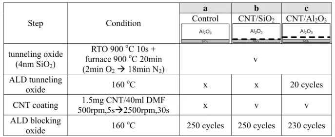
In this thesis, non-volatile memory devices utilizing CNT charge trapping layers are discussed. Devices for electrical characterization are listed below:
Sample a. MOSFET control samples with Al2O3/SiO2 gate stack
Sample b. CNT-memory devices with Al2O3/CNT/SiO2 gate stack
Sample c. CNT-memory devices with Al2O3/CNT/Al2O3/SiO2 gate stack
Other samples are prepared for material analysis such as SEM, AFM, and SCM. For these purposes, two kinds of samples are prepared.
Sample d. samples with CNT coating on SiO2 surface
Sample e. samples with CNT coating on Al2O3 surface
Some of the samples are deposited with a thin ALD Al2O3 layer for the SCM measurement.
Split conditions are summarized in Table 3-1 and 3-2.
3-2 Device Structure
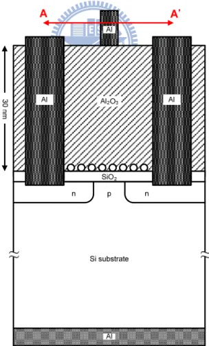
Fig. 3-1 is the top view of our MOSFET structure. The gray block is active area. Outside of that is field-oxide (FOX) region with about 400 nm oxide isolation. The black squares are contact holes of source/drain where aluminum is deposited. The black region including a line that crosses the neck of active area is the pattern of aluminum gate.
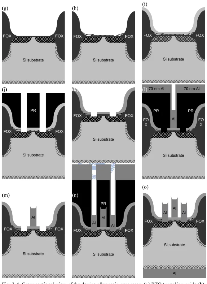
3-3 Process Flow
First, a standard LOCal-Oxidation-of-Silicon (LOCOS) process was performed and active area had been defined. After source/drain implantation, an RCA clean was performed and rapid thermal oxidation (RTO) was used for SiO2 tunneling oxide growth. Then, a 900 ℃
furnace annealing was used to improve the SiO2/Si interface quality and the tunneling layer
had a final thickness about 4 nm. Till this step, all front-end processes were finished without any difference between samples.
After tunneling oxide growth, different procedures were performed. CNT powder was first dissolved in dimethylformamide (DMF) and then spin-coated onto both SiO2 and Al2O3
surfaces. Solutions were sonicated for 24 hours before casting. Atomic layer deposition (ALD) was used to deposit Al2O3 layers after CNT coating. The total thickness of Al2O3 layer was
about 30 nm.
Before the densify step, source/drain contact holes were etched by BOE. A 20 minutes of N2 annealing at 700 ℃ was performed after the contact etching in order to densify ALD layers.
Contact holes were finally filled with 70 nm thermal evaporated aluminum and patterned by lift-off method. Metal gate was also formed with 70 nm thermal evaporated aluminum by lift-off step. Finally, wafer-back oxide was removed and a 400 nm aluminum layer was deposited as substrate contact for all the devices.
More details of the processes are described below:
Front-end steps: LOCOS, source/drain implantation and tunneling oxide growth 1. 6-inch Si wafer and laser marking
Boron doped 6-inch p-type silicon wafers were commercially obtained from Wafer Works Corp (http://www.waferworks.com). Laser marking was used for labeling. After that, an SC-1 cleaning was performed to remove the particles produced during laser marking. SC-1 is an abbreviation for “standard clean solution #1.” It is a step of soaking wafers into 75 ℃ solution of NH4OH : H2O2 : H2O = 0.25 : 1 : 5 for 600 seconds.
2. Pre-furnace standard clean and furnace dry oxide 35nm
The standard clean step includes solutions SC-1 and SC-2. Quick dump rinse (QDR) steps were performed before and after each cleaning step. SC-2 is a step of soaking wafers into 75 ℃ solution of HCl : H2O2 : H2O = 1 : 1 : 6 for 600 seconds. Dry oxidation was
performed by horizontal furnace to grow a screen oxide for the following ion implantation and also acts as the pad oxide of the following nitride layer.
3. Wafer back ion implantation
This ion implantation process produces an ohmic contact between Si-substrate and the wafer-back aluminum layer. BF2 ion at 60 keV to a dose of 5x1015 cm-2 dose was used.
4. Zero-layer marking
The zero-layer contains alignment marks for the following lithography processes. TEL MK8 Clean Track System was used for photo-resist (PR) coating and development. Canon FPA-3000 i5+ I-line Stepper was used for exposure. All the lithography steps of the devices were accomplished by these systems. After PR patterning, a dry etching was performed by TEL TE5000 Etcher.
5. Pre-furnace standard clean and LOCOS hard mask: furnace nitride 150nm
After another standard clean step, a 150 nm Si3N4 layer was deposited by a horizontal
low-pressure chemical vapor deposition (LPCVD) furnace
6. Field oxide region patterning and etching
The active area was defined by dry etching. TEL TE5000 Etcher was used to etch through nitride layer and left about 10 nm pad oxide acting as screen oxide of the next ion implantation step. After etching step, PR was removed by Mattson AspenII Asher and SPM (H2SO4 : H2O2 = 4 : 1, 120 ℃, 600 sec).
to a dose of 2x1013 cm-2. All of the ion implantation steps in this thesis were performed by Varian Ion Implant System E220HP or E500HP Implanters.
8. Field oxide formation: furnace wet oxide 550nm
After channel stop implantation, a pre-furnace standard clean was performed and then horizontal furnace grown 550 nm wet oxide was formed as the field oxide isolation.
9. Nitride hard mask wet etching and pad oxide removal
Hot phosphoric acid (~165℃) was used to remove the nitride hard mask after field oxide growth. Dilute HF was used to remove the pad oxide.
10. Pre-furnace standard clean and wet oxidation for white ribbon effect elimination
A 30nm wet oxidation was performed to eliminate the “white ribbon effect” and also to be the screen oxide of the next source/drain ion implantation step.
11. Source/drain implantation, and furnace activation
Source/drain was defined as in Fig. 3-1 with channel region protected by photo-resist. Source/drain implantation was done by phosphorus ions (P+) to a dose of 5x1015 cm-2 at 50 keV. Since devices in this thesis utilized metal gate process without self-align property as poly-gate, a longer annealing period should be performed to ensure an overlap between gate and source/drain region. For that reason, a 900 ℃ 30 minutes annealing in nitrogen ambiance was performed.
12. RCA clean, RTO tunneling oxide growth and Furnace annealing
After source/drain formation, tunneling oxide would then be formed. To avoid auto-doping effect from source/drain to channel region, a thin SiO2 film was first grown by
rapid thermal oxidation (RTO) before the furnace annealing. RTO-oxide provides a diffusion barrier preventing dopant out-diffusion from source/drain during the long thermal period in furnace. HEATPAULSE AG-610i Rapid Thermal Processing System was used for the 900 ℃/10 sec RTO. The annealing, first 2 min in oxygen then 18 min in nitrogen, both at 900 ℃, improved the interface quality of RTO-oxide and silicon substrate thus offers a
better electrical characteristics. The oxide thickness after annealing is about 4 nm.
Back-end steps: spin-coating, ALD, source/drain contact and metal gate 13. Spin-coating CNT
There are different ways to get CNT involved in a conventional semiconductor process. Generally, researchers would utilize chemical vapor deposition (CVD) to grow nanotubes [33] on the surface with metal catalyst coated. Nevertheless, direct growth of CNT would bring some problems to the study of CNT charging ability. For example, metal catalyst residues may also trap charges and confuses our judgment. To eliminate impurities without damage nanotubes is very difficult. Moreover, CNT growth is a complicated process and required sophisticated techniques. That brings many unnecessary difficulties to the research in this topic. Thus in this thesis, CNT was utilized and directly casted.
CNT powder grown by catalytic CVD commercially obtained from Nanostructured & Amorphous Materials Inc. (http://www.nanoamor.com) contains >95 vol% CNTs and >90 vol% SWNTs with outer diameter 1-2 nm and length ~15 μm. About 0.5 mg as-received powder was first dissolved into 40 ml N,N-Dimethylformamide (DMF). After 24 hours of sonicating, 2-step spin-coating was performed. The rotation of the first step was slower, in order to uniformly spread the solution on the whole wafer. The following high-speed step was for the purpose of removing redundant solutions on the surface. The rotation speeds are 500 rpm for 5 seconds and 2500 rpm for 30 seconds, respectively. After spin-coating, wafers were baked at 120 ℃ on the hot-plate for 3 minutes to further evaporate the residuary solvent.
14. ALD Al2O3 deposition
CNT, many studies has shown that good ALD layers are also difficult to grow. Due to CNT’s very perfect and inert exterior surface, the precursor’s adsorption is difficult. Thus typically a uniform ALD layer coating on CNT would require some kind of functionlization [34-36]. However, in this thesis, nanotubes were lying on the dielectric surface instead of suspending above some trenches; precursors could first adsorb on the oxide surface and then gradually piled up. Lateral growth would take place and finally make a complete cover of CNTs.
Trimethylaluminium (TMA) and H2O were the ALD precursors for Al2O3 film. Wafers
were placed on a quartz chuck and heated to 160 ℃ during the deposition. The growth rate was about 0.13 nm/cycle, and each cycle contains one pulse of each precursor and a nitrogen purge between the pulses. Total 250 cycles was performed on each wafer. CNT was placed at the planned position in the gate stack.
15. Source/drain contact patterning and wet etching
BOE dipping for 60 seconds was used to etch through the Al2O3/SiO2 layer with total
thickness about 40 nm. This step should be done before the densification step, because after that, the Al2O3 layer would be too strong for BOE to etch. The topography was measured
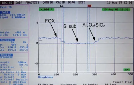
after etching using P-10 Surface Profiler. Fig. 3-3 shows a surface profile after BOE etching. Field oxide, gate dielectric, and silicon substrate are clearly shown in the picture.
16. Furnace annealing: ALD Al2O3 densification
After ALD Al2O3 deposition, a 30 minutes 700 ℃ N2 annealing was used to densify and
strengthen the Al2O3 film.
17. Gate metal deposition and lift-off patterning
Gate definition was also done by i-line lithography system. Gate lengths spread from 1 μm to 50 μm. A 70 nm aluminum film was deposited by the ULVAC EBX-6D Thermal Evaporation Coater. After that, wafers were sonicated in acetone for 5 minutes. Photo-resists and metal above it were lifted-off and left metal gate patterns.
18. Contact metal deposition and lift-off patterning
After another contact patterning process, the same aluminum thermal evaporation and lift-off process as for metal gates were performed to form source/drain contacts.
19. Wafer back contact metal deposition
To obtain a good back contact, a 400 nm aluminum layer was deposited by thermal coater after removing the native oxide. Till this step, the whole process was completed. Fig. 3-4 shows the device cross-sectional illustration of the whole process flow.
3-4 Operation Principles of Scanning Capacitance Microscopy (SCM)
Scanning capacitance microscopy (SCM) is a variant of scanning probe microscopy (SPM). It uses a metallic tip scanning across sample surface and measuring the capacitance between the tip/oxide/silicon. SCM was developed mainly for the purpose to determine the carrier concentration in micro-areas [37]. In this thesis, SCM is used for the charge detection in dielectric layers.
A simple illustration of SCM implementation is shown in Fig. 3-5 [38]. An SCM system contains a capacitance sensor added to a normal AFM system operating in contact mode. SCM can offer capacitance signal and topographic information simultaneously. The capacitance sensor employed in the very first SCM experiment [39] was originally developed by RCA for the purpose of “VideoDisc” reading operation [40]. Although there might be some modifications, capacitance sensors used in today’s SCM system still follow the basic concepts of that prototype.
An illustration of capacitance sense circuit in SCM system is shown in Fig. 3-6 [41]. The sensor is basically an LCR resonant circuit with an ultra-high frequency (UHF) oscillator. The
acts as an analog filter with a band-pass property. While metallic tip contacts with the sample surface, the tip/sample capacitance is incorporated into the LCR circuit and cause a shift of its resonant frequency, as shown in Fig. 3-7[42]. This shift in the response property causes an amplitude change of LCR circuit’s output signal. Thus, the tip/sample capacitance could be determined by measuring this output amplitude variation.
Ideally, the capacitance is able to be measured by the technique mentioned above. However, low frequency noise of the sensor circuit is usually very strong and should be eliminated. Thus a high frequency modulation signal together with a lock-in amplifier is used to filter out the noise [41]. This ac modulation signal is typically 1V peak-to-peak at 5-80 kHz [38] (in our case, its amplitude is 1V and frequency is 50 kHz). It alternately changes semiconductor surface between accumulation and depletion states. The lock-in amplifier measures the magnitude and phase of the sensor’s output voltage, rectify and amplify it into the final SCM signal, which is proportional to the differential tip/sample capacitance (dC/dV).
The major force which keeps pushing SCM’s evolution is the urgent need for a reliable carrier/dopant profiling tool in IC industry. Due to the close relation between C-V characteristic and the doping level of semiconductor surface, and also because of a rather simple way of sample preparation, SCM is expected to be a very useful technique. As the schematic illustration shown in Fig. 3-8a [43], the lower the doping level, the higher the differential capacitance signal. Also, the sensed differential capacitance signal has 180° phase shift between n-type and p-type doping, as shown in Fig. 3-8b [43]. Thus doping with opposite types might generate SCM signals with opposite signs.
SCM can be operated in two modes. When scanning in the open-loop mode, SCM uses an ac modulation signal with constant amplitude and measures the variation in differential capacitance signals. Higher doping concentration induces smaller change in the depletion width during ac modulating and hence a smaller change in capacitance would be observed at the same modulation amplitude, just as what mentioned above. Another way, called close-loop
mode, connects SCM system to a feedback circuit which controls the modulation amplitude and keep the differential capacitance signal constant. Instead of proportional to differential capacitance, the output signal of a close-loop SCM would be the amplitude of the modulation biases. Close-loop operation has the virtue that the volume of depletion area under the tip remains constant and therefore independent of the doping concentration. On the other hand, areas with lower doping concentration might have larger depletion area and degrades the spatial resolution in the open-loop mode.
Charges trapped in the dielectric layer will change the surface potential and shift Vth.
Thus SCM can be used to detect charges in the micro-area under the tip. Moreover, SCM tip can also apply voltages and change the quantities of charges underneath. Although many researches had use SCM to analyze the charge storage effects in different materials [44-46], this is the first time SCM being used on CNT charge storage analysis.
We had first try SCM on CNT-memory devices on sample band c right after ALD Al2O3
deposited. However, results were poor. Because capacitance is reversely proportional to dielectric thickness, SCM signal was too weak to be observed in the field oxide region with thickness of hundreds of nanometers. Under this limitation, active area was the only place could be scanned. Also, the higher doping concentrations, the lower SCM signal. Thus highly doped source/drain regions were impracticable, too. Finally, the gate dielectric larger than 30 nm used in our CNT-memory devices were found to be too thick to obtain clear SCM signal.
Thus, new samples designed especially for SCM measurements were prepared as following steps:
1. p-type silicon wafer
6. ALD Al2O3 growth, 50 cycles and 30 cycles on sample d and e, respectively
7. wafer back oxide removal 8. SCM measurement
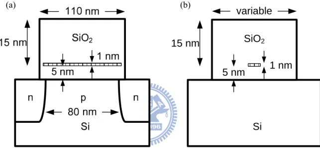
3-5 Numerical Simulation Settings
Technology computer-aid-design (TCAD) tool used in this thesis is Synopsys ISE TCAD 10.0. Two cases are discussed in this thesis, as shown in Fig. 3-9: a single charged wire parallel or perpendicular to source-drain direction crossing the channel. Some parameters were set to be variables in our simulation:
1. Storage type: positive or negative charge 2. Widths of trapping layer
3. Widths of channel
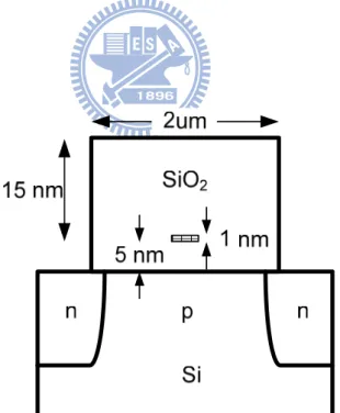
2D simulation was used to study case 1 while 3D simulation was used for case 2. Fig. 3-10 shows the structure settings of 2D simulation. An n-MOSFET with 20 nm SiO2 gate
dielectric is inserted with a 1 nm thick silicon nanowire as trapping material. The nanowire is 5 nm above the channel with 1 nm width. Gate length is 2 μm, overlaps with source/drain region 0.1 μm. Device structure settings in the 3D simulation are similar to those in the 2D case. As shown in Fig. 3-11a and 3-11b, channel length is 80 nm and width is variable.
Table 3-1. Experimental settings of samples for electrical characterization.
a b c
Step Condition Control CNT/SiO2 CNT/Al2O3
tunneling oxide (4nm SiO2) RTO 900 oC 10s + furnace 900 oC 20min (2min O2 Æ 18min N2) v ALD tunneling oxide 160 oC x x 20 cycles CNT coating 500rpm,5sÆ2500rpm,30s 1.5mg CNT/40ml DMF x v v ALD blocking
oxide 160 oC 250 cycles 250 cycles 230 cycles
Table 3-2. Experimental settings of samples for material analysis
d e
Step Condition
CNT/SiO2 CNT/Al2O3
thermal oxide RTO 900 oC 10s v
Al2O3 layer ALD 160 oC x 20 cycles
CNT coating 500rpm,5sÆ2500rpm,30s 1.5mg CNT/40ml DMF v Samples for SCM scanning had the additional steps below
Al2O3 layer ALD 160 oC 50 cycles 30 cycles
densification furnace 700 oC 20 min v
Al2O3
SiO2
Al2O3
Fig. 3-1. Top-view of the MOSFET device used in this thesis.
Fig. 3-3. Surface profile image obtained from P-10 profiler after the contact etching process step. The lowest area is the contact region etched by BOE dipping. Some of the Al2O3/SiO2
layers at the edge of contact hole were reserved as expected according to the mask design
(a) (b)
(d)
(c)
(f) (e)
PR Si substrate FOX FOX PR PR Si substrate 70 nm Al 70 nm Al Al FO X FO X PR Si substrate Al Al Al FOX FOX Si substrate Al Al Al Al FOX FOX (n) (m) (j) (o) (k) (i) (l) (g) (h)
Fig. 3-4. Cross sectional view of the device after main processes. (g) RTO tunneling oxide (h) spin-coating CNT (i) ALD Al2O3 (j) S/D contact etching (k) ALD Al2O3 densification (l) gate
patterning and gate metal (Al) deposition (m) gate metal lift-off (n) S/D contact patterning and contact metal (Al) deposition (o) S/D contact metal lift-off and wafer back metal deposition
Fig. 3-5. Block diagram of the scanning capacitance microscopy (SCM) system [38].
Fig. 3-7. Output characteristics of capacitance sensor [42].
Fig. 3-8. Examples of CV curves and SCM signals. (a) SCM signals on surfaces with different doping levels. (b) SCM signals on surfaces with different doping types. [43].
Fig. 3-9. Cases discussed in the TCAD simulation. (a) A CNT crosses channel and parallel to source-drain direction. (b) A CNT crosses channel and perpendicular to source-drain direction.
(a) (b)
Fig. 3-10. Structure settings of 2D simulation. An n-MOSFET with 20 nm SiO2 gate
dielectric is inserted with a 1nm thick silicon nanowire as trapping layer. The nanowire is 5 nm above the channel with a variable width. Gate length is 2um and
_
variable
_
1 nm
5 nm
15 nm
SiO
2Si
Fig. 3-11. Structure settings of the 3D simulation. An n-MOSFET with 20 nm SiO2
gate dielectric is inserted with a 1nm thick silicon bar as trapping layer. The silicon bar is 5 nm above the channel with a variable width. Channel length is 80 nm and width is variable.
Chapter 4
Results and Discussion
4-1
Microscopic Analysis
4-1.1 Scanning Electron Microscopy (SEM)
SEM images shown in this thesis were obtained by HITACHI-S-6280H in-line SEM system and FEI Nova 200 Dual beam (focused ion beam & electron beam) System. Wafers could be loaded on the in-line system without cleavage. This property brings a huge advantage when dealing with wafers still under fabrication. A typical setting of the in-line SEM system is 700 V accelerating voltage with emission current of about 10 μA. For the dual beam system, the accelerating voltage and emission current were set at 5 kV and 0.4 nA, respectively. Dual beam system has much higher resolution but is only available for small samples.
Spin-coating is a crucial step of our device fabrication, thus different process conditions had been tried. Some points were concerned in this step:
1. Raw CNT material conditions: purity, length distribution, etc. 2. Solution properties: solvent and concentration.
3. Spin-coating conditions: spinning rates and durations. 4. Surface materials.
Fig. 4-1a and 4-1b show the coating results using CNT powders with different purities (50~70 % and 95 % of CNT, respectively). Under the same coating conditions (on SiO2 surface, 500
contains >95 vol% CNTs and >90 vol% SWNTs and Fig. 4-2a is its coating results.
In addition to using high purity materials, an appropriate solution recipe is also indispensible. Fig. 4-2 shows a comparison in coating results between an over-dense solution and a lighter one (5 mg/40 ml and 0.5 mg/40 ml, respectively), both on SiO2 surfaces with the
same spin-coating steps as mentioned above. The over-dense solutions would lead to the formation of large CNT clusters. Aggregations would destroy the desired unique properties of CNT and should be avoided. In Fig. 4-3, with higher magnification, we can clearly observe that these clusters consist of huge quantities of nanotubes and no other impurities are involved.
Wettability of the solution is also of concern. A good solvent for spin-coating process needs not only high solubility of CNTs but also well wettability on the sample surface.
Surface material is an important factor also. We found that with the same solution and coating condition, CNTs spread much well on Al2O3 surface than on SiO2 surface as shown in
Fig. 4-4a and 4-4b. On SiO2 surface, CNTs tend to aggregate together and two distinct regions
were created: areas with over-dense coating and areas without any CNT existed. This situation is unsuitable for device fabrication. On the other hand, a uniform coating on Al2O3 without
aggregation is shown in Fig. 4-4b. By roughly counting the number of CNTs in the 4 μm x 4 μm black square shown in Fig. 4-4b, the density is about 2.8 tubes/μm2.
4-1.2 Atomic Force Microscopy (AFM)
Although SEM is a very convenient tool for surface inspection, it still has limitations on surface topography and roughness measurement. For these purposes, atomic force microscopy (AFM) was used. All AFM images shown in this thesis were performed by the Veeco Dimension 3100 Scanning Probe Microscope.
Fig. 4-5a and 4-5b show AFM images of CNT coating on SiO2 and Al2O3 surfaces. A
with SEM results. Because of the electron scattering effect in SEM and the poorer lateral resolution due to nm-scale AFM tip radius, vertical data obtained from AFM is a very important information to determine CNT’s (single, bundle, or cluster) size. Topography analysis (Fig. 4-5) shows that CNT clusters detected on SiO2 surface have typical sizes of
about tens to hundreds of nanometers, while the single or bundled CNTs shown on Al2O3
surface are usually 1-10nm high.
4-2
Electrical Characterization
Electrical characterization has been performed with different measurement conditions. First, gate voltage (Vg) sweeps from small range (e.g. -3 V to +3 V) to larger range (e.g. -15 V
to +15 V) were performed to observe the memory window and original state of each device. After these sweeps, the program and erase (P/E) speeds would be evaluated. Different gate biases were applied and the threshold voltage (Vth) shifts under these conditions were
measured. Program voltages were set to be positive, while negative voltages were used to erase the device back to its original state. The applied P/E stresses were asymmetric to Vg = 0
V, partially due to Vth of P/E states are usually asymmetric Vg = 0 V and also because of the
difference in P/E speeds depend on trapping levels. To evaluate erase speeds, devices were first programmed to a certain Vth shift and then erased by different biases. Finally, the
endurance and retention properties were also measured. For endurance measurements, selected P/E voltages were alternatively applied. After a number of cycles, Vth on P/E states
were recorded. For retention measurements, devices were first programmed to a certain state, held for a period of time, and then measured the Vth values. There’s one thing should be
two retention measurements is also necessary. The conditions of samples under measurement are listed below again:
Sample a. MOSFET control samples with Al2O3/SiO2 gate stack
Sample b. CNT-memory devices with Al2O3/CNT/SiO2 gate stack
Sample c. CNT-memory devices with Al2O3/CNT/Al2O3/SiO2 gate stack
First, by applying a continuous gate voltage sweep from -15 V to +15 V for several times, devices on sample a (the control sample) show no hysteresis loop, as shown in Fig. 4-6. This result confirms that any variation in the electrical properties on the other samples is totally originated from the inserted CNTs.
As mentioned in the previous section, we’ve found that CNT coating on Al2O3 surface
has a better dispersion quality and nanotubes are uniformly distributed on every device on sample c. By comparing the results of a series of devices on sample b and c, a consistent phenomenon was observed. Electrical characteristics of six adjacent devices with the same dimension on sample b and c are shown in Fig. 4-7a and 4-7b, respectively. In Fig. 4-7a, only one device shows an obvious memory window and the rest has nearly no Vth shift under ±15
V gate voltage sweeping. Compared with the SEM results, we found that devices with nothing shown in the channel region under SEM observation would also show nothing in their memory properties. On the other hand, all of the devices on sample cshow considerable memory windows.
There’s something should be emphasized: the hysteresis loop is counterclockwise. A positive program bias would induce positive charges in the gate stack and cause a negative Vth
shift, while a negative erase stress would bring it back to the original state. This property is consistent with the results of other studies [9][11][47][48], but inconsistent with another report [10]. Unlike typical non-volatile memories such as floating-gate or SONOS which electron injection occurs when positive gate biases are applied, the positive charge storage properties of CNT-memories are very special and worth further investigation.
P/E speed of sample b and c are shown in Fig. 4-8 and Fig. 4-9, respectively. The program speed of sample b is much faster than erase speed, comparing Fig. 4-8a and 4-8b. A +10 V Vg bias for 1 sec results in a -8 V Vth shift, and a +12 V Vg bias for 0.01 sec reaches the
maximum Vth shift about -10 V. For erasing, gate biases should be held for more than 1 sec to
make a distinct change. Completely erasing required -20 V Vg bias for more than 10 sec. Erase
voltage higher than -25 V will shift Vth of erase states toward negative (-Vg) direction and thus
become impracticable. On sample c, program speed is slower than sample b. A +12 V program bias for 1 sec could only create a -4 V Vth shift, while a -20 V bias for 1 sec could
shift Vth backward for 6V. The difference in the P/E speed will be explained later.
Endurance properties are shown in Fig. 4-5a and 4-5b. P/E conditions were set to be +12 V 0.1 sec/-20 V 1 sec and +20 V 1 sec/-20 V 0.5 sec for sample b and c, respectively. The memory window is quite stable for sample b. The Vth of P/E states are around -2 V and +2 V
with a 3-4 V shift. This situation persists even after 1000 cycles of operation. However, for sample c (Fig. 4-5b), the memory window start to shrink after 400 cycles of operation, from 6 V to 3 V. This result shows that the program speed degraded after 400 cycles of operation (Vth
of program state shift toward +Vg direction while Vth of erase state keep stable).
Retention properties of sample b and c are shown in Fig. 4-6a and 4-6b. The amounts of stored charges in sample b and c reduced to about 80 % and 50 % after 105 seconds, respectively. By extrapolation, their memory windows are expected to reduce to about 7 V (60 % of the initial window) and 0.7 V (7 % of initial window) after ten years. The result of sample b is comparable to Ryu’s report (58 % and 16 % of stored charges remain after 10 years, for standing and lying SWNTs devices respectively). [10]
4-3
Charge Storage Mechanisms
4-3.1 SCM analysis
Sample preparation for SCM analysis is described as following. First, 4 nm SiO2 layer
was grown on the p-type silicon wafer by rapid thermal oxidation (HEATPAULSE AG-610i Rapid Thermal Processing System) at 900 ℃ for 10 sec in oxygen ambiance. Then, a thin Al2O3 film (~3 nm) was deposited by ALD. After that, CNT-contained DMF solution was
dispersed onto sample surface. The same coating condition as in our device fabrication was used here. Another Al2O3 film (~4 nm) was then deposited by ALD and finally a 700 ℃
furnace annealing was performed to densify these ALD films. Before placing the sample onto SCM chuck, wafer-back was brushed with BOE solution to remove oxide layers and form an ohmic contact of silicon substrate. A simple illustration of our sample under SCM measurement is shown in Fig. 4-12.
An ac signal with 1 V amplitude and 50 kHz frequency was used in our SCM measurement. The resulting images were composed of SCM signal at 0 V dc bias on each point. As the color-bar shows, positive SCM signals will be displayed in black and purple colors and negative signals will be displaced as yellow or red colors. Green color indicates ambiguous SCM signals.
Fig. 4-13 shows the topography image captured simultaneously as SCM images were obtained. The quality of this image is poorer than our previous AFM results because the metal layers coating on SCM tip increases its radius and largely degrades the lateral resolution. In this thesis, the Ti/Pt coated silicon tip has radius of about 40 nm, which is larger than that of the probe used for AFM analysis (commercially obtained from MikroMasch, see: http://www.spmtips.com). Vertical analysis shows that the linear regions with CNT underneath are typically 5 nm higher than the background. This result is similar to that obtained by AFM analysis.
Comparing Fig. 4-14a and 4-14b, an obvious connection between AFM and SCM image could be detected. Regions with CNT underneath show completely different signals from background. Negative SCM signals were detected in these regions and caused many red ribbons appear in the green background. In the first image (Fig. 4-14b), all regions with CNT underneath are red. While scanning again and again, some of these regions started to change their colors, from red to purple. By placing the tip on top of surface with CNT underneath and sweeping the dc bias (which is applied from the substrate) from +3 V to -3 V and backward, a hysteresis loop was detected, as shown in Fig. 4-15. This loop represents a charge variation in the scanning region. Also, the counterclockwise hysteresis is consistent with the memory characteristics of our devices shown in previous part. Both are positive charge storage after positive gate stresses.
4-3.2 Possible Mechanisms
Some properties shown in Fig. 4-14 are worth discussion. First, signal changes are only detected in the regions with CNT underneath. This is the direct evidence that memory effect of our devices is completely caused by CNTs, not other impurities. The slightly darkening of green background is might due to the scrape of Al2O3 surface by contact-mode SCM tip.
Secondly, the individual CNT is not at equal potential. Since CNT is conductive, this observation indicates that instead of free charges stored in the CNT, the charge storage effects are more likely due to other local mechanisms. Also, only positive charge storage under positive gate bias was detected, and for both sample b and c, program speeds are faster than erase speeds. Possibilities of different mechanisms are discussed below:
5. electric field-induced carrier injection from CNT
The most common explanation of charge storage effect in non-volatile memory devices should be carriers transport between electrode, channel, and dielectric layers. From our experimental results, that should be hole-injection from gate electrode to CNTs or adjacent traps, as shown in Fig. 4-16a. However, the blocking oxide is 30 nm thick and tunneling oxide is less than 5 nm. It’s hard to believe that holes can transport through a thick blocking layer while electrons were less possible to transport through the thin tunneling layer.
Mobile ions and organic molecules might also cause positive charge storage effect (Fig. 4-16b and 4-16c). However, mobile ions seem to be unlikely in our case with fast program speed under room temperature. On the other hand, memory effect attributed to polar molecules might have symmetric Vth shift from original state, which is different from our case
that Vth only shift in –Vg direction.
Some papers had reported that positive charges might also come from interfacial defects caused by electron injection and the following hydrogen release and trapping [49], as shown in Fig. 4-16d. However, this theory couldn’t answer the question how these positive charges could be erased.
Carrier injection from CNT might be the most possible explanation. As described in ref. 26, due to the electric field near CNT is enhanced to a level comparable to dielectric’s breakdown field, carriers might inject from CNT to the traps in dielectric nearby. As describe in Fig. 4-16e, when +Vg is applied during program period, the large field at SiO2/CNT
interface induces hole-injection from CNT to traps in SiO2. These injected holes may migrate to deeper traps. When –Vg is applied during erase period (Fig. 4-16f), deeper trapped holes
would be slower to be erased. Thus explained the slower erase speed compared to program speed. Also, most of the color-changed regions shown in SCM results were not reversely erased back. This is because erasure usually requires higher voltage than program operation due to the asymmetric Vth of P/E states and different energy barriers for trapping/detrapping
mechanisms
4-4 Numerical simulation
From the SCM results, we know that charges are locally stored around the CNT. This local charge storage effect causes a completely different memory behavior to normal memory devices which charges cover the whole channel region. Some simulations were taken to study the device behavior under these situations.
The simulation settings were already discussed in chapter 3, and simulated structural results are shown in Fig. 4-17 and 4-18.
Different quantities of charges with opposite signs were place in the nanowire and electrical characteristics were simulated. Results are shown in Fig. 4-19a and 4-19b. When the wire is negatively charged, on-current of the n-MOSFET would be easily suppressed (Fig. 4-19a), while the same amount of positive charges cannot affect electrical characteristics (Fig. 4-19b). This property can be easily illustrated by the potential diagram shown in Fig. 4-20a and 4-20b. A small area of barrier rising caused by negative charges can block most of the on-current, while a small barrier lowering caused by positive charges cannot increase the off-current.
For the case while charged wire is parallel to the channel, different effects were observed. A positive charge line along source-drain direction would induce a narrow conducting path underneath and device would be partially turned-on under this condition. The advanced conducting region under nanowire is shown in Fig. 4-21a and 4-21b, the profiles of electron current density and electron density, respectively. The electrical characteristics are shown in Fig. 4-22. Because only part of the channel is advanced turned on, the conducting current is
For a negative charged line along the same direction, however, the effect is hard to detect: a narrow region with higher Vth would not affect the whole electrical characteristics.
Different channel widths were tried in the positive charge case, in order to determine under what condition a kink in Id-Vg curve might appear, as we saw in Fig. 4-7. As shown in
Fig. 4-23, a clear kink could be observed when channel width is larger than 1000 times of nanowire width, and a full shift of Id-Vg curve appears as soon as channel width smaller than
200 times of nanowire width.
In conclusion, the polarity of charge and the direction of trapping wire are both important parameters that affect device’s memory behavior. Positive charges have no effect when the trapping wire is perpendicular to source-drain direction, while negative charges cannot be detected when the wire is parallel to source-drain direction.
Based on our simulation results, we found that only positive charge storage existed in our experiment. Although negative charge might be invisible in some cases, e.g. small CNT coverage ratio of channel width, still no phenomenon appeared when device were fully covered by CNT. According to our simulation, negative charges can have strong effects on electrical characteristics when charged regions cross the channel. Thus no negative charges stored in the CNT-memory devices were confirmed. Also, the simulation shows that when positive charges cover the partial width of channel, a partially shift of Id-Vg curve might be
seen and a kink would be detected. That consisted with our experimental results, e.g. Fig. 4-7b. According to our simulation, different CNT alignments should be designed to match different polarities of stored charges.
Fig. 4-1. (a) SEM image of CNT coating with lower-purity CNT powder. Many catalyst particles could be observed around CNTs. (b) SEM image of CNT coating with higher-purity CNT powder. No catalyst particle is observed.
Fig. 4-2. (a) SEM image of CNT coating with over-dense concentration. Large clusters with thousands of CNTs could be observed. (b) SEM image of CNT coating with proper
(a) (b) (a) (b)
Fig. 4-3. Magnified SEM image of a CNT cluster which could be seen in Fig. 4-2a. We can clearly observe a huge quantity of nanotubes without many impurities.
Fig. 4-4. (a) SEM image of CNT coating on SiO2 surface. (b) SEM image of CNT coating on
Al2O3 surface.
Fig. 4-5. (a) AFM image of CNT coating on SiO2 surface. (b) AFM image of CNT
coating on Al2O3 surface.
(a)
-15
-10
-5
0
5
10
15
10
-1110
-1010
-910
-810
-710
-610
-510
-4I
d(A)
V
g(V)
(-15,+15,-15)
(-15,+15,-15)
(-15,+15,-15)
(-15,+15,-15)
Fig. 4-6. A ±15V gate voltage sweeping result of a device on sample a (MOSFET control samples with Al2O3/SiO2 gate stack)
![Fig. 2-2. Illustration of the chiral vectors of CNT on an imaginary graphene plane [17]](https://thumb-ap.123doks.com/thumbv2/9libinfo/8410358.179816/23.892.166.743.225.552/fig-illustration-chiral-vectors-cnt-imaginary-graphene-plane.webp)
![Fig. 3-6. Block diagram of the capacitance sense circuit in SCM system [41].](https://thumb-ap.123doks.com/thumbv2/9libinfo/8410358.179816/38.892.201.733.561.914/fig-block-diagram-capacitance-sense-circuit-scm.webp)
![Fig. 3-7. Output characteristics of capacitance sensor [42].](https://thumb-ap.123doks.com/thumbv2/9libinfo/8410358.179816/39.892.277.653.190.503/fig-output-characteristics-capacitance-sensor.webp)