IEEE ELECTRON DEVICE LETTERS, VOL. 26, NO. 7, JULY 2005 467
Performance and Reliability of Poly-Si TFTs on
FSG Buffer Layer
Shen De Wang, Student Member, IEEE, Tzu Yun Chang, Chao Hsin Chien, Member, IEEE, Wei Hsiang Lo,
Jen Yi Sang, Jam Wen Lee, and Tan Fu Lei
Abstract—A novel and process-compatible scheme for
fabri-cating poly-Si thin-film transistors (TFTs) on an FSG buffer layer was proposed and demonstrated. Experimental results reveal that remarkably improved device performance and uniformity can be achieved with appropriate fluorine concentration. The poly-Si TFTs fabricated on FSG layers have a higher on-current, a lower leakage current, and a higher field-effect mobility compared with the conventional poly-Si TFTs. Furthermore, the incorporation of fluorine also increased the reliability of poly-Si TFTs against hot carrier stressing, which is attributed to the formation of Si–F bonds.
Index Terms—Buffer layer, fluorine, fluorinated silicate oxide
(FSG), polycrystalline silicon thin-film transistors (poly-Si TFTs), reliability.
I. INTRODUCTION
P
OLYCRYSTALLINE silicon thin-film transistors (poly-Si TFTs) have attracted much attention owing to the pos-sibility of realizing the integration of driving circuits and pixel elements on a single glass substrate, and the potential to accomplish the system-on-panel (SOP) [1]. High-perfor-mance and high-reliability poly-Si TFTs are required to reach this goal. Excimer laser annealing (ELA) has been utilized in enlarging the grains of the poly-Si to reduce trap states, leading to an excellent device performance [2]. However, the random distribution of grain boundaries in poly-Si films still causes a large leakage current and poor device uniformity. Hydrogenation process has been utilized to terminate the grain boundary trap states [3]. However, hydrogenated poly-Si TFTs suffer from an instability issue due to weak Si–H bonds [4]. On the other hand, a low-temperature plasma-enhanced chemical vapor deposition (PECVD)-oxide buffer layer is conventionally adopted to block the contaminations from the inexpensive glass or flexible plastic substrate. Nevertheless, the mismatch be-tween the thermal expansion coefficient of the poly-Si and that of the oxide causes considerable mechanical tensile stress at the interface during ELA, leading to the degradation in device performance [5]–[8]. All these drawbacks limit the applications of poly-Si TFTs. Recently, fluorine atoms have been proposedManuscript received March 23, 2005; revised April 18, 2005. This work was supported by the National Science Council, Taiwan, R.O.C., under Contracts NSC 93-2215-E-009-003 and NSC 93-2215-E-009-036. The review of this letter was arranged by Editor J. Sin.
S. D. Wang, T. Y. Chang, W. H. Lo, J. Y. Sang, and T. F. Lei are with the Department of Electronics Engineering and Institute of Electronics, National Chiao-Tung University, Hsinchu 300, Taiwan, R.O.C.
C. H. Chien and J. W. Lee are with the National Nano Device Laboratories, Hsinchu 300, Taiwan, R.O.C.
Digital Object Identifier 10.1109/LED.2005.851242
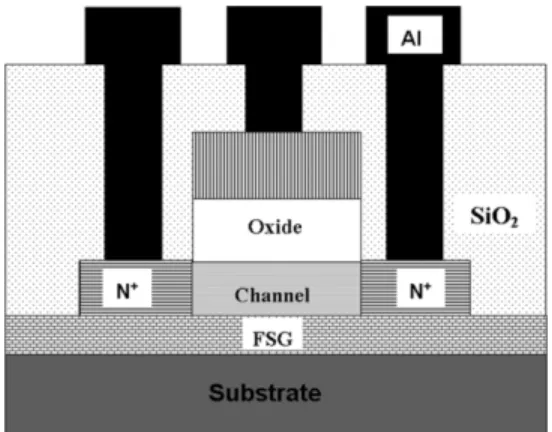
Fig. 1. Cross section of the proposed poly-Si TFT fabricated on a FSG buffer layer.
to terminate trap states in the poly-Si [9]–[12]. The formation of Si–F bonds improves the device reliability. However, ion implantation is not appropriate for extremely large-sized glass substrate in current productions.
Therefore, a new method must be found to introduce fluorine atoms into poly-Si films. Fluorinated silicate oxide (FSG) has been known easy to integrate using PECVD systems. The out-diffused fluorine atoms form FSG can terminate trap states and also release the strain bonds at the interface [13]. This letter pro-poses a novel process-compatible fluorination technique using a FSG film as the buffer layer. The Poly-Si TFTs fabricated on FSG buffer layers exhibit high device performance, uniformity, and reliability.
II. EXPERIMENTAL
Fig. 1 schematically depicts the cross section of the proposed poly-Si TFT. All the experimental devices in this letter were fabricated on thermally oxidized Si wafers. First, a 50-nm-thick FSG buffer layer was deposited using a PECVD system at 350 C with SiH , CF , and N O as process gases. To deter-mine the effect of fluorine content in FSG layers, varying CF flow rates of 10, 20, and 40 sccm, with a SiH flow rate of 90 sccm and a N O rate of 5 sccm, were used to grow various FSG buffer layers, denoted by FSG1, FSG2, and FSG3, respec-tively. The fluorine contents in FSG1, FSG2, and FSG3 were about 2%, 4%, and 7%, respectively. Then, 100-nm-thick amor-phous silicon layers were deposited on the FSG layers in a low-pressure chemical vapor deposition (LPCVD) system. Next, a semi-Gaussian-shaped KrF excimer laser nm with an energy density of 420 was performed for the phase transformation from amorphous to polycrystalline silicon. The
468 IEEE ELECTRON DEVICE LETTERS, VOL. 26, NO. 7, JULY 2005
Fig. 2. Transfer characteristics of the poly-Si TFTs fabricated on various buffer layers. The inset shows the SIMS profiles of fluorine in the poly-Si on various buffer layers.
average grain size of the poly-Si is approximately 300 nm. In-dividual active regions were then patterned and defined. After a clean process, a 100-nm-thick TEOS oxide and a 200-nm-thick poly-Si were deposited to serve as the gate insulator and the gate electrode. A self-aligned phosphorous ion implantation was pre-formed at the dosage and energy of 5 cm and 40 keV, respectively. The dopant activation was performed by ELA, fol-lowed by a deposition of passivation layer and the definition of contact holes. Finally, a 500-nm-thick Al electrode was de-posited and patterned. For comparison, the control samples were fabricated on a 50-nm-thick conventional PECVD-oxide buffer layer.
III. RESULTS ANDDISCUSSION
Fig. 2 shows the transfer characteristics of the conventional and the proposed poly-Si TFTs at V. The poly-Si TFTs fabricated on the FSG buffer layers exhibit better on-state and off-state characteristics than those of the control sample. Notably, under a large negative gate bias, the leakage currents of the TFTs on FSG layers are over one order of magnitude lower than that on the conventional oxide buffer layer. This is ascribed to the facts that the reduced the traps by the incor-poration of fluorine in the poly-Si films during ELA [12] and the released tensile stress at the poly-Si/buffer-oxide-layer in-terface [13]. The evidence of the fluorine incorporation can be firmly demonstrated with the SIMS profiles of fluorine shown in the inset of Fig. 2. It was clearly observed that considerable fluorine atoms were detected in the poly-Si for the FSG sam-ples and, in particular, two fluorine peaks were located at the top and bottom interfaces. Therefore, we believe that the weak bonds and dangling bonds in the poly-Si grain boundaries and both top and bottom interfaces, resulting in lots of trap states and interface states, were terminated by fluorine [10]. In order to verify the effect of fluorine passivation, the effective trap
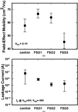
Fig. 3. (a) Distributions of field-effect mobility and (b) leakage current of the poly-Si TFTs on different buffer layers. The vertical bars indicate the minimum and maximum values of the devices characteristics and the squares are the average values.
state density was calculated from the square root of the
slope of the versus plots, which was
proposed by Proano et al. [14]. The for the control, FSG1, FSG2, and FSG3 were 5.64 , 3.91 , 3.97 , and 4.01 cm , respectively. These figures strongly hint that the fluorine can effectively terminate the present trap states. However, the FSG3 shows a detrimental effect on the perfor-mance of the resulting TFT. This is attributed to the moisture absorption. According to previous report, the moisture absorp-tion increased with increasing fluorine content in the FSG layers [15]. The absorbed moisture would easily form OH or react with fluorine to form HF, which in turn corrode the devices and result in the degraded performance and reliability [16].
Fig. 3 displays the statistical distributions of the field-effect mobility and the leakage current of the poly-Si TFTs fabricated on different buffer layers. The vertical bars in the figure indicate the minimum and maximum values of the devices characteristics and the squares present the average values. The average values of the for the control, FSG1, FSG2, and FSG3 samples were 57.7, 66.7, 63.9, and 45.2 with standard deviations of 4.05, 2.98, 3.09, and 4.15, respectively. This tendency indicates that with moderate fluorine content in FSG layers the average values and the deviations of can be greatly improved. Also, the average values of the for the control, FSG1, FSG2, and FSG3 samples were 6.8 , 7.8 , 1.3 , and 1.8 with standard deviations
of 8.14 , 2.46 , 6.55 , and 1.93 ,
re-spectively. The uniformity of the poly-Si TFTs is strongly af-fected by the random distribution of grain boundaries. There-fore, using fluorine to terminate those trap states can effectively alleviate the influence of grain boundaries.
WANG et al.: PERFORMANCE AND RELIABILITY OF POLY-SI TFTs 469
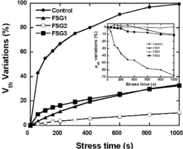
Fig. 4. Variations of threshold voltage as a function of stress time under hot carrier stress. The inset shows the variations of field-effect mobility as a function of stress time under hot carrier stress.
Hot-carrier-stress was performed at V and V for 1000 s to investigate the device relia-bility. Fig. 4 plots the variations of threshold voltage and over hot carrier stress time. The variations of
and were defined as –
and – , respectively, where
, , , and represent the
mea-sured values before and after stress. Notably, the control shows relatively large variations in both and after 1000s stress, whereas the FSG2 stays almost unchanged. These results imply that poly-Si TFTs fabricated on the FSG layer greatly reduced the device degradation under hot carrier stress, which is due to the formation of the Si–F bonds. Since the calculated percent-ages of F content in the FSG layers are 2%, 4%, and 7% for FSG1, FSG2, and FSG3, respectively, we deduce based on the above experimental results that the trap states can be effectively terminated when the fluorine content in the FSG is above 2%; while the absorbed moisture in the FSG as the content is above 4% starts to induce visible corrosion of the poly-Si structures after competing with the trap states termination. Definitely, the corrosion becomes more severe as the content reached 7%. As a result, the optimized condition of fluorine content of FSG is probably within 2% to 4%.
IV. CONCLUSION
A novel process-compatible scheme for fabricating poly-Si TFTs on an FSG buffer layer is proposed. Significant improve-ments in the device performance and uniformity were success-fully demonstrated with fluorine incorporation in the poly-Si layer. The incorporation of fluorine also promotes the
hot-car-rier immunity. Fabricating poly-Si TFTs on FSG buffer layers with appropriate fluorine content improves not only the elec-trical performance and uniformity but also the reliability.
REFERENCES
[1] T. Serikawa, S. Shirai, A. Okamoto, and S. Suyama, “Low-temperature fabrication of high-mobility poly-Si TFTs for large-area LCDs,” IEEE
Trans. Electron Devices, vol. 36, no. 9, pp. 1929–1933, Sep. 1989.
[2] G. K. Guist and T. W. Sigmon, “High-performance thin-film transistors fabricated using excimer laser processing and grain engineering,” IEEE
Trans. Electron Devices, vol. 45, no. 4, pp. 925–932, Apr. 1998.
[3] I. W. Wu, W. B. Jackson, T. Y. Huang, A. G. Lewis, and A. Chiang, “Pas-sivation kinetics of two types of defects in polysilicon TFT by plasma hydrogenation,” IEEE Electron Device Lett., vol. 12, no. 5, pp. 181–183, May 1991.
[4] , “Mechanism of device degradation in n- and p-channel polysilicon TFTs by electrical stressing,” IEEE Electron Device Lett., vol. 11, no. 4, pp. 167–170, Apr. 1990.
[5] E. Fujii, K. Senda, F. Emoto, A. Yamamoto, A. Nakamura, Y. Uemoto, and G. Kano, “A leaser-recrystallization technique for silicon-TFT in-tegrated circuits on quartz substrates and its application to small-size monolithic active-matrix LCDs,” IEEE Trans. Electron Devices, vol. 37, no. 1, pp. 121–127, Jan. 1990.
[6] M. Cao, S. Talwar, K. J. Kramer, T. W. Sigmon, and K. C. Saraswat, “A high-performance polysilicon thin-film transistor using XeCl excimer laser crystallization of pre-patterned amorphous Si films,” IEEE Trans.
Electron Devices, vol. 43, no. 4, pp. 561–567, Apr. 1996.
[7] K. Kitahara, A. Moritani, A. Hara, and M. Okabe, “Micro-scale char-acterization of crystalline phase and stress in laser-crystallized poly-Si thin films by Raman spectroscopy,” Jpn. J. Appl. Phys., vol. 38, pp. L1312–1314, 1999.
[8] S. Higashi, N. Ando, K. Kamisako, and T. Sameshima, “Stress in pulsed-laser-crystallized silicon films,” Jpn. J. Appl. Phys., vol. 40, pp. 731–735, 2001.
[9] H. N. Chern, C. L. Lee, and T. F. Lei, “The effects of fluorine passivation on polysilicon thin film transistors,” IEEE Trans. Electron Devices, vol. 41, no. 5, pp. 698–702, May 1994.
[10] S. Maegawa, T. Ipposhi, S. Maeda, H. Nishimura, T. Ichiki, M. Ashida, O. Tanina, Y. Inoue, T. Nishimura, and N. Tsubouchi, “Performance and reliability improvement in poly-Si TFTs by fluorine implantation into gate poly-Si,” IEEE Trans. Electron Devices, vol. 42, no. 6, pp. 1106–1112, Jun. 1995.
[11] J. W. Park, B. T. Ahn, and K. Lee, “Effects ofF implantation on the characteristics of poly-Si films and low-temperature n-ch poly-Si thin-film transistors,” Jpn. J. Appl. Phys., vol. 34, pp. 1436–1441, Mar. 1995.
[12] C. H. Kim, S. H. Jung, J. S. Yoo, and M. K. Han, “Poly-Si TFT fabricated by laser-induced in situ fluorine passivation and laser doping,” IEEE
Electron Device Lett., vol. 22, no. 8, pp. 396–398, Aug. 2001.
[13] Y. Mitani, H. Satake, Y. Nakasaki, and A. Toriumi, “Improvement of charge-to-breakdown distribution by fluorine incorporation into thin gate oxides,” IEEE Trans. Electron Devices, vol. 50, no. 11, pp. 2221–2226, Nov. 2003.
[14] R. E. Proano, R. S. Misage, and D. G. Ast, “Development and electrical properties of undoped polycrystalline silicon thin-film transistors,” IEEE
Trans. Electron Devices, vol. 36, no. 9, pp. 1915–1922, Sep. 1989.
[15] H. Miyajima, R. Katsumata, Y. Nakasaki, Y. Nishiyama, and N. Hayasaka, “Water absorption properties of fluorine-dopedSiO films using plasma-enhanced chemical vapor deposition,” Jpn. J. Appl. Phys., vol. 35, pp. 6217–6225, 1996.
[16] G. Passemard, P. Fugier, P. Nobl, F. Pries, and O. Demolliens, “Study of fluorine stability in fluoro-silicate glass and effects on dielectric proper-ties,” Microelectron. Eng., vol. 33, pp. 335–342, 1997.