國立交通大學
電子工程學系 電子研究所碩士班
碩 士 論 文
p 型金氧半電晶體反轉層電洞遷移率
的物理計算
Physics-Based Calculation of Hole Inversion-Layer
Mobility in pMOSFETs
研 究 生:簡 鶴 年
Ho-Nien Chien
指導教授:陳 明 哲 博士
Prof. Ming-Jer Chen
p 型金氧半電晶體反轉層電洞遷移率的物理計算
Physics-Based Calculation of Hole Inversion-Layer Mobility in
pMOSFETs
研 究 生:簡 鶴 年 Ho-Nien Chien
指導教授:陳 明 哲 博士 Prof. Ming-Jer Chen
國立交通大學
電子工程學系 電子研究所碩士班
碩 士 論 文
A Thesis
Submitted to Department of Electronics Engineering &
Institute of Electronics
College of Electrical and Computer Engineering
National Chiao Tung University
in Partial Fulfillment of the Requirements
for the Degree of
Master of Science
In
Electronics Engineering
July 2008
Hsinchu, Taiwan, Republic of China
p 型金氧半電晶體反轉層電洞遷移率
的物理計算
研究生:簡鶴年 指導教授:陳明哲 博士
國立交通大學
電子工程學系 電子研究所碩士班
摘 要
在過去的數十年中,為了追求高積集度、高速度、以及低功率消耗的元件表 現,互補式金氧半場效電晶體的元件尺寸不斷地被縮小。此篇研究論文的目的是 根據元件量子物理的觀念,針對一個 p 型的金氧半場效電晶體,在其形成反轉層 時對等效的電洞遷移率建立了一個簡單的計算模型,並將程式模擬的結果和"普 適曲線"的實驗結果做比較。 較詳細的次能帶結構計算可以由 k∙p 的方法求解一維的薛丁格和波松方程 式得到。而在我們的模型裡面,我們使用了求解 4×4 Luttinger-Kohn 矩陣的特 徵值的方法來得到修正過的次能帶結構。除此之外,我們使用了等效質量的模型 分別去推算量子化等效質量、能態密度等效質量以及導電度等效質量。 我們考慮了三個散射模型:聲學聲子散射、光學聲子散射和表面粗糙度散射。最終,我們建立了一個等效的電洞遷移率模型並將結果和 Takagi 教授在不 同溫度下的實驗結果做比較。
Physics-Based Calculation of Hole Inversion-Layer
Mobility in pMOSFETs
Student:Ho-Nien Chien Advisor:Dr. Ming-Jer Chen
Department of Electronics Engineering
Institute of Electronics
National Chiao Tung University
ABSTRACT
In pursuit of high integration density, high speed and low power consumption, complementary metal-oxide-semiconductor (CMOS) devices have been undergoing a progressive down-scaling strategy over the past few decades. The purpose of our study is to build a simple hole mobility model in the inversion layer of a p-type metal-oxide-semiconductor field effect transistor (pMOSFET) based on quantum device physics and compare the results with the experimental data on the so called universal curves.
A detailed subband structure calculation is obtained by solving the one-dimensional Schrodinger and Poisson equations with a six-band k‧p procedure. In our model, however, we have used a modified subband structure which is actually the solution of the eigenvalue problem in a 4×4 Luttinger-Kohn matrix. Besides, we have also used an equivalent effective mass model to derive the quantization-direction
effective mass, the density-of-states effective mass, and the conductivity effective mass.
Three scattering mechanisms are included in our model: acoustic phonon scattering, optical phonon scattering, and surface roughness scattering. Finally, we build a modified hole mobility model and compare the calculation results with Takagi’s data for various temperatures.
Acknowledgements
本論文得以完成,首先非常感謝陳明哲教授對我的細心指導與諄諄教誨,讓 我學習到研究的正確態度以及撰寫論文的大方向。另外,研究其間亦承蒙中興大 學電機系張書通教授對研究內容提供指導與建議也在此同表謝意,並感謝口試委 員們-李文欽先生與張智勝先生提供的寶貴建議與指教。 論文撰寫過程中特別感謝建志學長所給予的建議與協助。此外,感謝博士班 學長的指導與照顧:振宇學長、智育學長、及韋漢學長等;感謝實驗室的同學們 -立方、以唐、悌華、彥銘、佳弘、東壕,以及學弟們-侑穎、又正、以東在課 業和日常生活上總是相互的扶持,幫忙實驗室裡大大小小的事,讓我們能更專心 於研究工作。 最後,我要感謝我的家人和曾經幫助過我的人,你們所給予的支持是我完成 論文最大的原動力。謹將我的成果與喜悅獻給所有關心我的家人、老師與朋友們。
Contents
page
Chinese Abstract
………...i
English Abstract
………..iii
Acknowledgements………...
v
Contents
………vi
Figure Captions……….
vii
Table Captions………...
ix
Chapter 1 Introduction……….…...
..1
Chapter 2 Hole Mobility Model and Theory………….……...
2
2.1 Numerical Solutions of Schrodinger Equation…….…...….
.2
2.2 Luttinger-Kohn Hamiltonian and Subband Structure….………..4
2.3 Newton-Raphson Method……….…………6
2.4
Equivalent Effective Masses……….………...9
2.5
Phonon Scattering Mechanisms……….……….11
2.6
Surface Roughness Scattering Mechanisms………...13
2.7
Derivation of Two-Dimensional Mobility……….…….16
Chapter 4 Conclusion………
22
References………..
23
Figure Captions
Fig.1 A potential profile in which a wavefunction is confined.
………..
26
Fig.2 Illustration of the energy band diagram of a pMOSFET operating in inversion mode. Vs is the surface bending potential and z direction is the direction orthogonal to Si/SiO2 interface.
………..………
27
Fig.3 Schematic illustration of Newton–Raphson method for finding successively better approximations to the zeros (or roots) of a real-value function.
………….
28
Fig.4 The flow-chart illustrating the self-consistent calculation procedure.
…....
29
Fig.5 Density of states for the first HH, LH, and SO subband, numerically computed at the effective electric field orthogonal to the Si/SiO2 interface equals to
1MV/cm. The solid line shows the density of states derived in the effective mass approximation (EMA).
…………...………..
30
potential energy at the centroid is approximately raised by EeffΔ.
...
31
Fig.7 Plot of Γ
( )
q and γ( )
q . The ratio Γ( )
q /γ( )
q is approximately constant over the q range of interest.………...
32
Fig.8 Average spatial extent of the inversion layer carriers from the surface, zav, as
a function of the total density of inversion and depletion charges for (100) Si at T=300K and T=77K.
...
33
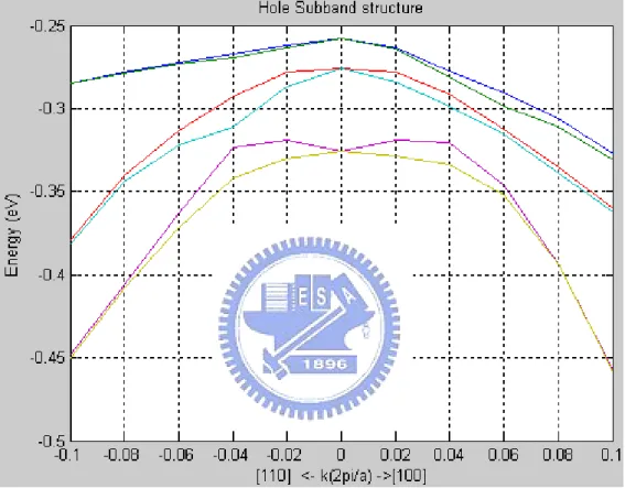
Fig.9 Unstressed subband E-K relation, where Eeff = 1 MV/cm.
…………...
34
Fig.10 The extracted equivalent quantization-direction effective mass (mz) for
heavy-hole, light-hole and split-off hole.
………..……….
35
Fig.11 Three dominant scattering mechanisms at high effective electric field and the corresponding mobility component with the substrate donor doping concentration ND=1.6x1016cm-3 and temperature T=300K.
……….…..
38
Fig.12 The simulation results of two-dimensional hole mobility and comparison with the experimental data of Takagi [2] in three different temperatures of 77K, 153K, and 300K.
………...………...……….
39
Table Captions
Table 1 List of the quantization-direction effective mass (mz), density-of-states
effective mass (mDOS), and conductivity effective mass (mc) for the heavy-hole (HH),
light-hole (LH), and split-off hole (SO).
………....
36
Table 2 Surface roughness scattering parameters used in our work and comparison to the values recently reported in the literature.
………
37
Chapter 1
Introduction
The MOSFETs (metal-oxide-semiconductor field effect transistors) technology has undergone a scaling-down strategy in recent years. As the device channel length shrinks towards nanometer level and below, the underlying assumptions of the conventional MOSFET scaling rule are rapidly losing validity. However, the incorporation of strain engineering and the use of alternative materials are being regarded as a potential way to maintain or even improve the device performance.
Despite the great quantities of recent researches devoted to the experimental investigation of pMOS transistors [3], [4], the development of the numerical simulators for pMOSFETs which have the ability to explore the physical properties of the two-dimensional hole gas in the inversion layer suffers a lag with respect to the nMOSFETs counterpart. In this study, we place an emphasis on building a thorough effective hole mobility model of pMOSFETs, and compare the simulation results with experimental data. It is noticeable that we have made some simplified assumptions so that the overall computational complexity of our model can be dramatically lowered compared to a fully numerical treatment. Our approximation seems to be reasonable because of the fairly good agreements with the experimental data for three distinct temperatures.
Chapter 2
Hole Mobility Model and Theory
2.1 Numerical Solutions of Schrodinger Equation
For an arbitrary potential profile in which a wavefunction is confined as shown in Fig. 1, the general Schrodinger equation Eq. (1) can be expressed in terms of a matrix equation. This approach is very useful if we are looking for bound or quasi-bound states in a spatially varying potential V. Let us assume that the eigenfunction we are looking for is confined in a region L as shown in Fig. 1. We divide this region into equidistant l mesh points xi, each separated in real space by a distance Δx. The
wavefunctionΨwe are looking for is now of the form
(1) 2 2
2
−
∇
V
E
m
Ψ + Ψ = Ψ
n n (2) n aψ Ψ =
∑
where
ψ
n is simply the function at the mesh point, normalized within the intervalcentered at
x
n and being zero outside that interval. We can also write the differentialequation as a general difference equation
(
)
(
)
( )
(3) 2 2 1 1 2 2 i i i z z z V E m z Ψ − + Ψ + − Ψ ⎡ ⎤ ⎢ Δ ⎥ ⎣ ⎦ − + Ψ = ΨOnce again, substituting for the general wavefunction Eq. (2) and taking an outer product with
ψ
1,ψ
2, · · · ,ψ
l, we get a set of l equations (assumea
0 =a
l+1 = 0, i.e.,the wavefunction is localized in the space L), which can be written in the matrix form as
(4)
( )
( )
( )
( )
1 1 2 2 3 3 0 0 0 0 0 0 0 0 0 0 0 0 l l l A z B a B A z B a B A z a B A z a ψ ψ ψ ψ ⎡ ⎤ ⎡ ⎤ ⎢ ⎥ ⎢ ⎥ ⎢ ⎥ ⎢ ⎥ ⎢ ⎥ ⎢ ⎥ 1 2 3 = ⎢ ⎥ ⎢ ⎥⎢⎢ ⎥⎥ ⎢ ⎥ ⎢ ⎥ ⎢ ⎥ ⎢ ⎥ ⎢ ⎥ ⎢ ⎥ ⎣ ⎦ ⎣ ⎦ with (5)( )
( )
2 2 i i z V z E m z = + − Δ A(6) 2 2
This l × l set of equations can again be solved by calling an appropriate subroutine from a computer library to obtain the eigenvalue En and wavefunction
ψ
n. In generalwe will get l eigenvalues and eigenfunctions. The lowest lying state is the ground state, while the others are excited states.
2
B= −
2.2 Luttinger-Kohn Hamiltonian and Subband Structure
In the calculation of the hole mobility in the inversion layer, Schrodinger equation and Poisson equation are solved self-consistently to simulate the potential energy in the channel. The subband structure and the two-dimensional density-of-states (2D DOS) function of each subband are calculated with which the scattering relaxation time can be evaluated. Finally, 2D hole mobility is obtained from a linearization of the Boltzmann equation.
Fig. 2 sketches the energy band diagram of a pMOSFET operating in inversion mode. We can write the 1D Schrodinger and Poisson equations as follows [5]:
⎣
⎡
H K k
ˆ
0(
,
z)
+
IV z
( )
⎤
⎦
⋅
ψ
K( )
z
=
E K
n( ) ( )
ψ
Kz
(7)( )
(8) 2 2 i s d V z dzρ
ε
= −For Si pMOSFETs, holes are confined in the z-direction quantum well formed by the Si/SiO2 interface and the valence band edge. Since the hole energy is not
continuous along z-direction, kz should be replaced by 1
i z
∂
∂ . Besides, we can express
the potential V(z) as –Eeff
z
because of the triangular potential approximation. Afterundergoing a transformation of the basis, the Hamiltonian in the Schrodinger equation would be transformed to the Luttinger-Kohn Hamiltonian.
(9)
(
)
(
)
(
)
(
)
2 0 / 3 2 0 2 3 2 2 / 2 0 2 0 / 2 3 0 2 2 3 / 2 0 2 2 2 LK P Q R R S S 2 2 R P Q Q S S R Q P S S H S S P Q R R S S R P Q S S R Q P + + + + + + + + + + + ⎡− + − ⎤ ⎢ ⎥ ⎢ − − − − ⎥ ⎢ ⎥ ⎢ ⎥ ⎢ ⎥ − − − Δ − ⎢ ⎥ ⎢ ⎥ = ⎢ − − + − − ⎥ ⎢ ⎥ ⎢ − − − − ⎥ ⎢ ⎥ ⎢ ⎥ ⎢ ⎥ − − − ⎢ ⎥ ⎣ ⎦Finite element method is utilized to compute Schrodinger and Poisson equation numerically. We divide the analysis area into a z mesh of Nz points in the interval
(0,Zmax), where
z
max is the sum of the thickness of silicon layer and oxide layer. This would yield a 6Nz x 6Nz eigenvalue problem, which can be expressed as thetridiagonal block form
(10) Q − − Δ 1 1 l l l − + ⎤ ⎡ ⎤ ⎥ ⎢ ⎥ ⎢ ⎥ ⎢ ⎥ ⎢⋅ ⋅⎥ ⎢ ⎥= ⎢ ⎥ ⎢⋅ ⋅⎥ ⎢ ⎥ ⎢ ⎥ ⎢ ⎥ ⎢ ⎥ ⎢ ⎥ ⎢⋅ ⋅ ⋅ ⋅ ⋅ ⋅ ⋅⎥ ⎢ ⋅ ⎥ ⎢ ⋅ ⎥ ⎣ ⎦ ⎣ ⎦ ⎣ ⎦
( )
0 1 1 0 0 1 1 0 0 0 0 0 0 l l l l l l D D D E k D D D D D Dψ
ψ
ψ
ψ
ψ
ψ
− + − − − + − + + + ⋅ ⋅ ⋅ ⋅ ⋅ ⋅ ⋅ ⋅ ⋅ ⎡ ⎤ ⎡ ⎢⋅ ⋅⎥ ⎢ ⎢ ⎥where each ψ
( )
z is a six-component column vector. D+, D0, and D- are 6x6 block-diagonal difference operators expressed as belowH
2 (11)0 1 2
(12) H
( )
1 2 2 2 H i z z + Δ Δ D = −(13)
( )
0 2 0 2 2 l H D H z = + Δ2H1
( )
22 (14) H i z z − − Δ Δ D = −After calculating the eigenvalue problem in Eq. (10) with the aid of MATLAB, the desired hole subband E-k relation is obtained [5].
2.3 Newton-Raphson Method
The Newton–Raphson method (or Newton–Fourier method) is a well-known method for finding successively better approximations to the zeros (or roots) of a real-value function. Newton's method can often converge remarkably quickly, especially if the iteration begins “sufficiently near” the desired root. First of all, in Fig. 3, we start with an initial guess, for example, V0, and find the corresponing function
value R. Secondly, the function is approximated by its tangent line, and one computes the V-intercept of this tangent line (which is easily done with elementary algebra). This V-intercept will typically be a better approximation to the function's root than the
original guess, and the method can be iterated. This iteration process could be expressed as a mathematical formula:
V
n+1=
V
n+
R
/
R
' (15)If we write the 1D Poisson equation in Eq. (8) as an operator form
(16) 2 2 2 2 2 2 2 2 1 0 1 1 1 2 1 2 2 3 3 1 2 0 V V V ρ ⎡− ⎤ ⎢ Δ Δ ⎥ ⎡ ⎤ ⎡ ⎤ ⎢ ⎥ ⎢ ⎥ ⎢ρ ⎥ ⎢ − ⎥ = ⎢
(17)
(18)
(19) ρ ⎥ ⎢ ⎥ Δ Δ Δ ⎢ ⎥ ⎢ ⎥ ⎢ ⎥ ⎢ ⎥ ⎣ ⎦ ⎣ ⎦ ⎢ − ⎥ ⎢ Δ Δ ⎥ ⎣ ⎦
Let AV=ρ, where
2 2 2 2 2 2 2 2 1 0 1 2 1 1 2 0 A ⎡− ⎤ ⎢ Δ Δ ⎥ ⎢ ⎥ =⎢ − ⎥ Δ Δ Δ ⎢ ⎥ ⎢ − ⎥ ⎢ ⎥ ⎢ ⎥ Δ Δ ⎣ ⎦ 1 2 3 V V ⎡ ⎤ ⎢ ⎥ = ⎢ ⎥ ⎢ ⎥ ⎣ ⎦ V V 1 2 3 ρ ρ ρ ρ ⎡ ⎤ ⎢ ⎥ ⎣ ⎦ ⎢ ⎥ = ⎢ ⎥
In order to accelerate the calculation speed of self-consistent procedure, we apply Newton-Raphson method when solving Poisson and Schrodinger equations self-consistently. We can hence express the Poisson equation as follows:
R
= −
AV Rho
+
(20)' ' (21) 1 / n n dR dRho V V R R R = A dV dV + = + ⇒ = − +
Fig. 4 is the flow-chart illustrating the self-consistent procedure. First, we start with the 1D Schrodinger equation, as revealed in Eq. (7), along with an initial guess surface potential Vs and with the depletion region width d = 50 nm, or expressed as
V z
( )
E zeff Vs zd
= − = − (22)
As mentioned in Section 2.2, we would obtain the hole E-k relation and corresponding wavefunction if the potential profile is given in the 1D Schrodinger equation. Using the calculated E-k relation, we could derive the effective two-dimensional density-of-states (2D DOS) (see Section 2.4) and two-dimensional carrier density. Substituting the two-dimensional hole density in the 1D Poisson equation, we have
( )
( )
2 2 i i D dep S S ep z N d V z dz ρ ε ε ⎡ + ⎤ ⎣ ⎦ = − = − (23) where p2D( )
z is the two-dimensional hole density and is the depletion charge. Finally, we obtain a new potentialdep
N
( )
V z to satisfy Equation (23) and continuously iterate the procedure.
2.4 Equivalent Effective Masses
The quantization-direction effective mass mz in the direction orthogonal to the
Si/SiO2 interface has been extracted by comparing the lowest energy level E0 of each
subband (as obtained in Section 2.2) with the corresponding value given by the Airy formula [6], that is
(24) 1/ 3 2/ 3 2 2 2 0 3 0 9 9 2 z 8 z 2 8 eF eF E ⎛ ⎞ m m E
π
π
⎡ ⎤ ⎛ ⎞ =⎜ ⎟ ⎢ ⎥ ⇒ = ⎜ ⎟ ⎣ ⎦ ⎝ ⎠ ⎝ ⎠where F is the transverse electric field. Despite the fact that the band structure is field-dependent since the external field would lift the degeneracy of the valence band at the point, field dependence of the heavy-hole band is weak. We could choose a constant value of the quantization effective mass of heavy-hole equal to 0.29m
Γ
0 for
fields up to 1 MV/cm. On the contrary, the field dependence of the light-hole band is more sensitive. For most of our purposes, a constant mz of 0.23m0 has proven to be
accurate enough to describe the light-hole while both the field and doping dependences have been neglected [7], [14].
Empirical description of the warping close to the Γ point can be expressed as follows
(
)
(25) 2 2 2 4 2 2 2 2 2 2 2 0 2 EHH Ak B k C k kx y k ky z k kz x m ⎡ ⎤ = − ⎢ − + + + ⎥ ⎣ ⎦(
)
(26) 2 2 2 4 2 2 2 2 2 2 2 0 2 ELH Ak B k C k kx y k ky z k kz x m ⎡ ⎤ = − ⎢ + + + + ⎥ ⎣ ⎦Where A, B, and C are constants. In order to derive the two-dimensional density-of-states (2D DOS), we have made an intuitive assumption, i.e., let
cos x k =k θ , ky =ksinθ and kz = . 0 (27)
(
)
( )
2 2 2 4 2 4 2 2 ,2 0 cos sin 2 HH D = −2m ⎡⎣⎢ k − B k +C k θ θ ⎤⎥⎦=g θ k E A (28)( )
2 2 2 2 2 0 cos sin 2 g A B C m ⎡ θ θ⎤ = − ⎣ − + ⎦ θwhere g
( )
θ is a function independent of wavevector k. The number of states per unit area of k-space can be written as( )
2 2 2 2 D dk N π=
∫
[8]. In polar coordinate system, we obtain( )
2 2 2 2 2 1 1 4 4 2 D dk dE N kd dk dE dk θ θ π π π =∫
=∫∫
=∫∫
kd (29)( )
( )
2 2 2 0 0 1 1As a consequence, the two-dimensional density-of-states (2D DOS) can be expressed as the following form
(30)
The effective mass for the density of states, mDOS, has been derived from
4 2 4 E 2 dE d kd dE g k g π θ θ θ π θ π θ ∞ = = =
∫∫
=∫
∫
( )
( )
(
)
2 2 0 2 2 2 2 2 2 2 2 0 0 1 4 2 4 cos sin D m dN d d D E dE g A B C π π θ θ θ θ π = θ π = θ θ = = = − − +∫
∫
(31)
( ) ( )
( )
2 p v DOS p D E f E dE g m f E π∫
dE =∫
where the left hand side is the density of states occupied by holes. The function D(E) is the density of states and fp(E) is the hole occupation probability function. The right
hand side is instead the density of states for a parabolic band with an equivalent effective mass mDOS and gv being the band degeneracy [7]. The density of states
derived in effective mass approximation is shown in Fig. 5.
Note that we have neglected the electric field and doping dependences on the effective masses and regarded them as constant values, as summarized in Table 1.
2.5 Phonon Scattering Mechanisms
Carriers migrate through the crystal with properties determined by the periodic potential associated with the array of ions at the lattice points. Vibration of the ions about their equilibrium positions introduces interaction between electrons and the ions. This interaction induces transitions between different states. And this process is called phonon scattering. Phonon scattering can be categorized to acoustic phonon scattering and optical phonon scattering based on the phase of the vibration of the two different atoms in one primitive cell. Both contribute to the momentum relaxation time. Acoustic phonon energy is negligible compared with carrier energy, while optical phonon energy is about 61.3meV for silicon and 37meV for germanium at long wavelength limit.
Using the subband energy and the wavefunction provided by the self-consistent calculation, phonon-limited mobility, which consists of acoustic phonon mobility and optical phonon mobility, can be calculated under the momentum relaxation time (MRT) approximation. More precisely, for the acoustic phonons, the relaxation time in the band (i,j) is given by [9], [10] :
(32) (33)
( )
( ) ( )
(
)
2 , 3 2 , 1 2 2 , 1 ac 1 vk dk ac B i j ac l i j i j i j n m D k T E s W W z z dzτ
ρ
ξ
ξ
− = =∫
(34)( )
(
)
( )
, 1 j j i j j ac ac U E E E Eτ
τ
− =∑
where denotes the deformation potential due to acoustic phonon, is the valley degeneracy,
ac
D ac
vk
n
ρ is the mass density of the crystal, is the longitudinal sound velocity, is the form factor determined by the wavefunctions of the ith and the jth subbands and U(x) is the step function. Whereas for optical phonons, we have
l s , i j W (35)
( )
(36)(
)
(
( )
)
( ) ( )
(
)
' 2 ' , int 1 2 ' 2 , 1 1 1 1 2 2 1 dk m m vkk m m j i j m m er i j i j n m D f E E N U E E E E fρ
E E V z z dzτ
ξ
ξ
− − ⎛ ⎞ = ⎜ + ± ⎟× − × − ⎝ ⎠ =∑
∫
∓ ∓where “+” means phonon emission and “-“ means phonon absorption. k and k’=1, 2, and 3, meaning HH, LH, and SO, respectively. Dmf and Emf are the deformation potential and the energy of the mth intervalley phonon, respectively. N is the
occupation number of the mth intervalley phonon.
2.6 Surface Roughness Scattering Mechanisms
The physical meaning of the surface roughness may be briefly shown in the simple schematic illustration in Fig. 6 [11]. Let us assume that the interface is shifted by a quantity with respect to its average position. In the same region, the wavefunction will also be shifted by
Δ
Δ(dashed line). Therefore, the average potential at the centroid of the carriers is approximately raised by EeffΔ. It is well known that a
potential change would result in scattering and consequently act as a perturbation of carrier transport [11], [12].
Before entering a more detailed analysis, we have to make an important assumption that the single subband approximation is quite accurate. Since most of the holes are in the first subband, we have restricted our calculation to intrasubband transitions. The resulting formulation for the surface roughness relaxation time τSR is
(37)
where VSR
( )
q is the scattering matrix element. θ is the angle between the initial wavevector Ki = ( Ki ,θ) and the final wavevector Kj = ( Kj, θ β+ ). q is themagnitude of the wavevector change 2 2 2 2 cos
i j i j
q =k +k − k k θ . The scattering matrix
( )
(
)
'( ) (
)
(
( )
( )
2 ' 1 2 1 cos SR SR q k k V q E k E k E kπ
θ δ
)
= − =∑
− −τ
element VSR
( )
q has been implemented according to Ando’s model [13]. Ando constructed a more accurate model by taking the following two effects: the dipole correction to scattering potential, due to the oxide deviations from perfect planarity, and the effects of the image charges, due to the dielectric constant discontinuity at the SiO2/Si interface. Hence, the scattering matrix element is written as(38)
( )
( ) ( )
where is the wavevector-dependent dielectric constant accounting for the screening capability of the hole gas, i.e., we have modified the perturbing potential
( )
r q ε
( )
SR
V q by multiplying a correction factor 1/εr
( )
q . S q is a Gaussian power( )
spectrum of the surface roughness(39)
where and are the root-mean-square value of the asperities and the correlation length, respectively. The and values used in this work and their comparisons recently reported in other literatures are listed in Table 2.
Δ Λ
Δ Λ
( )
2 q
Γ contains all the remaining electrostatics (basically depending on ). By definition, 2 eff E
( )
2 qΓ can be expressed in terms of the wavefunction derivative at the SiO2 / Si interface located at z=0:
( )
2 2 SR r S q q q Γ = 2 V qε
( )
( )
2(
( )q 4/ 4)
e
π
− Λ=
ΔΛ
S q
( )
( )
( )
2 2 2 0 2 j i z z z d z d z q m dz dzξ
ξ
= ⎡ ⎛ ⎞⎤ Γ =⎢ ⎜ ⋅ ⎟⎥ ⎢ ⎝ ⎠⎥ ⎣ =0 ⎦ (40)It is noteworthy that the temperature has a strong dependence on the wavefunction. As a matter of fact, Γ
( )
q can be separated into two individual parts and summed up as follows:(41)
Γ
( )
q
=
γ
( )
q
+
γ
imm( )
q
The first term accounts for the potential perturbation due to real charges, while
( )
qγ
( )
imm q
γ is the correction due to their images. The term γ
( )
q can be written as eEeffΦ( )
q , where is a slowly varying function of q that decreases from one to( )
q Φ /ox Si
ε ε when q→ ∞. As shown in Fig. 7, γ
( )
q changes less than 25% when q spans from zero to 10 cm17 −1. We can therefore claim that shows alinear dependence on
( )
qγ eff
E approximately. According to Fig. 7, Since the ratio is nearly a constant over the q range of interest in the scattering problem, hence
( ) ( )
q /γ q Γ( )
qΓ can also be considered linearly dependent on Eeff .
According to Fig. 8, the average spatial extent of the inversion layer carriers from the surface would decrease when the temperature drops [6]. Hence the surface roughness scattering would become more noticeable at lower temperatures. In our surface roughness scattering model, we have introduced a temperature-dependent factor nfac, together with the linear dependence on
av
z
eff
obtain
(42)
where
(43)
(44)
Based on detailed calculations of the surface scattering matrix element VSR
( )
q [13], we have inferred a simple analytical formula accounting for the main functional dependencies of τSR on Eeff and temperature for holes. The two-dimensional mobility is derived in the following section.2.7 Derivation of Two-Dimensional Mobility
Since the inversion layer carrier in the MOS system is quantized along the out-of-plane direction, we must consider the quasi-2D case when calculating the mobility of the MOS system. Starting with the current density per unit length J ( J=I/W) and n the carrier concentration per unit area, we can write
( )
( ) ( )( ) ( ) 2 2 2 2 2 2 2 2 2 4 1 cos 0 2 3 01
sin
e
d
2
i d i m j E E d effect SRq m
E
E
πθ
θθ
τ
⎡ ⎤ ⎢ ⎥ − − Λ − ⎢ ⎥ ⎣ ⎦Δ Λ
=
∫
0 effect effE
=
nfac E
×
1 01
3
eff dep inve N
N
E
ε ε
⎛
+
⎞
⎜
⎟
⎝
⎠
=
(45)
(
)
2 2 2 / 4 2 2 x y x y fd k q nqv L L qv fvd k L Lπ
π π
= ⎛ ⎞ ⎜ ⎟ ⎜ ⎟ ⎝ ⎠∫
∫
= = J (46) 0(
)
0 f (47)where f0 is the Fermi-Dirac distribution function under equilibrium and f is the
first-order Taylor series expansion with respect to energy E, i.e., f is the Fermi-Dirac distribution function under applied electric field ε:
(48) where 0 22 4 d k q f π
∫
vi is zero since no current flows under equilibrium. Using theconcept of conductivityσ , the current can be expressed as follows:
( )
2 2 0 2 2 ( ) 4 ii i ii i f q v d E kσ
σ
τ
π
= ∂ = − ∂∫
i J ε (49) f f v q E τ ε ∂ = + − ∂ 1 0 E EF 1 e KT − + f = 2 2 2 2 0 0 2 2 2 2 0 2 2 4 ( )( ) 4 4 [ ( ) ( ) ] 4 i i i i qn f d k q f d k d k q f q q E f q d kπ
τ
π
Eπ
τ
π
= = ∂ = + − ∂ ∂ = − ∂∫
∫
∫
∫
i i i i i J v v v v ε v v εAccording to the relation between the conductivity and mobility, we obtain:
( )
( )
( )
( )
( )
( )
( ) (
)
( )
2 0 2 2 2 2 0 2 2 2 0 2 2 * 2 0 2 4 2 4 2 4 2 i i ii ii i d E E f q v E kdkd E nq n f k dEd f q E E g n f f q E d E E dE E g m f E dEτ
θ
σ
μ
π
θ
θ
τ
θ
π
θ
τ
θ
θ
π
π
∞ = ∂ ∂ = = ∂ ∂ = ∂ − ∂ =∫
∫
∫
∫
. (50)The details of the expression above are derived in the polar coordinate, and we have used the following definition:
2 2
( ) ( )
2
2( )
DOS D Dm
n
D
E f E dE
f E d
π
=
∫
=
∫
E
(51)( )
( )
2 2 22
iE E
g
k
dE
dE
kdkd
kd
kd
dE
g
k
dk
θ
θ
θ
θ
θ
−
=
⇒
∫
=
∫
=
∫
(52)v
1 E
f
( )
k
θ
k
∂
=
=
∂
(53)If we separate the θ-dependent terms and θ-independent terms from Equation (50), we could write the 2D mobility as follows:
( )
( )
( )(
)
0 2 2 2 2 2 0 0 24
2
2
i i i E E xx DOS E Ef
E E E dE
E
f
q
d
g
m
f
dE
π θτ
θ
μ
θ
π
θ
π
∞ = ∞ = =∂
−
∂
=
∫
∫
∫
( )
( )
( )(
)
2 2 0 2 0 02
2
i i i E E DOS c E Ef
f
E E E dE
q
d
E
g
q
m
m
f dE
π θθ
τ
θ
τ
θ
π
∞ = = ∞ =∂
−
∂
=
∫
∫
=
∫
(54)Finally, we could define the conductivity mass and the mean scattering time:
(55)
(56) Note that both f
( )
θ and g( )
θ have the units of the 1/ mass, som
DOS and has the same units of mass.c
m
( )
( )
2 2 22
θ 02
DOS cm
m
f
d
g
ππ
θ
θ
=
=∫
θ
( )(
)
( )
0 0 i i i E E E Ef
E E E dE
E
f E
∫
dE
τ
τ
∞ = ∞ =∂
−
∂
=
∫
Chapter 3
Simulation Results and Comparison
Based on simulated subband structure in Fig. 9, as mentioned in section 2.2, the equivalent effective masses i.e., quantization-direction effective mass (mz),
density-of-states effective mass (mDOS) and conductivity effective mass (mc) for
heavy-hole (HH), light-hole (LH) and split-off hole (SO) can all be extracted as shown in the following Fig. 10 and Table 1.
In accordance with the assumptions we have made when calculating the hole subband energy dispersion relation in the inversion layer of pMOS transistors, we further present a simplified physics-based model to describe the hole mobility, which mainly consists of the phonon-limited mobilityμph and the surface-roughness-limited mobility μsr. We have simulated many different cases with different substrate doping concentration and within a temperature range from 50K to 300K. The model parameters are: oxide thickness = 2.5nm, and poly doping concentration = 2.2x1020cm-3. Fig. 11 shows the mobility components for the substrate donor doping concentration ND = 1.6x1016cm-3 and temperature T=300K. According to
Matthiessen's rule, the total mobility,
μ
total, is described by1 1
total ph sr
1
μ
−=
μ
−+
μ
−. (57)
Fig. 12 shows the simulation results of two-dimensional hole mobility. We compare the simulation results with the experimental data of Takagi [2] in three different temperatures of 77K, 153K, and 300K. We adjust the model parameter by
fitting these data [2]: When T=77K and ND=2.7×1017cm-3, nfac=9; when T=153K and
ND=5.2×1015cm-3, nfac=5.4; and when T=300K and ND=1.6×1016cm-3, nfac=1.6. The
surface roughness parameters are Δ=2.7 Å and Λ=10.3 Å.
It is noticeable that there is a considerable deviation between simulation results and experimental data in low effective electric field region and at extremely low temperature. A reasonable physical explanation of this discrepancy is that we have eliminated Coulomb scattering mechanisms in our model. As mentioned in Section 2.6, surface roughness scattering would dominate the scattering mechanisms at low temperature, so the maximum nfac value occurs at the lowest temperature. If we plot nfac as a function of temperature, it could be shown that nfac drops quickly as the temperature increases from 50K to 300K. The minimum value of nfac is 1, which occurs at room temperature, as shown in Fig. 13. In our simplified model, we have replaced the calculation of the wavefunction derivative at the SiO2/Si interface located
at z=0 in Eq. (40) with a parameter nfac, which is a function of temperature. Hence, the computational complexity of our model is much smaller compared to a fully numerical treatment [10].
Chapter 4
Conclusion
In summary, we have presented a simplified model for the hole mobility in the inversion layer of pMOSFETs. The equations in the model and the physical meanings of its parameters are apparent. In fact, the parameters are extracted by best curve-fitting to the experimental data as cited in Takagi’s paper [2]. It is noticeable that at room temperature, our simulation results fit the experimental data well in the entire effective electric field range. However, at extremely low temperature, for example, 77K, there is a discrepancy in low effective electric field region. A possible explanation for this error is, according to the universal curves in [2], that phonon scattering becomes negligible and surface-roughness-limited mobility
μ
sr would dominate the scattering mechanism in high effective electric field region at low temperature, but the importance of Coulomb scattering would increase in low effective electric field region. However, Coulomb scattering was not included in our model.Among the many topics in the future research, some important ones could be listed as follows: mobility enhancement in strained-silicon pMOSFETs, and mobility enhancement in one-dimensional silicon nanowires since physical fluctuations (like surface roughness) has a strong impact on the transport of silicon nanowires.
References
[1] Y. T. Hou and Ming-Fu Li, “Hole Quantization Effects and Threshold Voltage Shift in pMOSFET—Assessed by Improved One-Band Effective Mass Approximation,” IEEE Trans. Electron Devices, vol. 48, no. 6, pp.1188-1193, June 2001.
[2] Shin-ichi Takagi, Akira Toriumi, Masao Iwase, and Hiroyuki Tango, “On the Universality of Inversion Layer Mobility in Si MOSFET's: Part I-Effects of Substrate Impurity Concentration,” IEEE Trans. Electron Devices, vol. 41, no.12, pp. 2357-2362,
Dec. 1994.
[3] L. Smith, V. Moroz, G. Eneman, P. Verheyen, F. Nouri, L. Washington, M. Jurczak, O. Penzin, D. Pramanik, and K. De Meyer, “Exploring the limits of stress-enhanced hole mobility,” IEEE Electron Device Lett., vol. 26, no. 9, pp. 652–654, Sep. 2005.
[4] Q. Xu, X. Duan, H. Qian, H. Liu, H. Li, Z. Han, M. Liu, and W. Gao, “Hole mobility enhancement of pMOSFETs with strain channel induced by Ge pre-amorphization implantation for source–drain extension,” IEEE Electron Device Lett., vol. 27, no. 3, pp. 179–181, Mar. 2006.
[5] M. V. Fischetti, Z. Ren, P. M. Solomon, M. Yang and K. Rim, “Six-band k·p calculation of the hole mobility in silicon inversion layers: Dependence on surface orientation, strain, and silicon thickness,” J. Appl. Phys., vol. 94, no. 2, pp.1079-1095, July 2003.
[6] T. Ando, A. B. Fowler, and F. Stern, “Electronic properties of two-dimensional systems,” Rev. Mod. Phys., vol. 54, pp. 437–672, Apr. 1982.
[7] Agostino Pirovano, Andrea L. Lacaita, Günther Zandler, and Ralph Oberhuber, “Explaining the Dependences of the Hole and Electron Mobilities in Si Inversion
Layers,” IEEE Trans. Electron Devices, vol. 47, no.4, pp. 718-724, April 2000.
[8] M. Lundstrom, Fundamentals of Carrier Transport (Cambridge University Press, Cambridge, UK, 1999) 2nd edn.
[9] Shin-ichi Takagi, Judy L. Hoyt, Jeffery J. Welser, and James F. Gibbons, “Comparative study of phonon-limited mobility of two-dimensional electrons in strained and unstrained Si metal oxide semiconductors field-effect transistors,” J. Appl. Phys., vol. 80, no. 3, pp.1567-1577, Aug. 1996.
[10] Marco De Michielis, David Esseni, Y. L. Tsang, Pierpaolo Palestri, Luca Selmii, Anthony G. O’Neill, and Sanatan Chattopadhyay, “A Semianalytical Description of the Hole Band Structure in Inversion Layers for the Physically Based Modeling of pMOS Transistors,” IEEE Trans. Electron Devices, vol. 54, no. 9, pp. 2164-2173, Sept. 2007.
[11] Gianluca Mazzoni, Andrea L. Lacaita, Laura M. Perron, and Agostino Pirovano, “On Surface Roughness-Limited Mobility in Highly Doped n-MOSFET’s, ” IEEE Trans. Electron Devices, vol. 46, no. 7, pp. 1423-1428, July 1999.
[12] David Esseni, “On the Modeling of Surface Roughness Limited Mobility in SOI MOSFETs and Its Correlation to the Transistor Effective Field,” IEEE Trans. Electron Devices, vol. 51, no. 3, pp. 394-401, March 2004.
[13] T. Ando, “Screening effects and quantum transport in a silicon inversion layer in strong magnetic fields,” J. Phys. Soc. Jap., vol. 43, pp. 1616–1626, 1977. [14] Tony Low, Yong-Tian Hou, and Ming-Fu Li, “Improved One-Band Self-Consistent Effective Mass Methods for Hole Quantization in p-MOSFET,” IEEE Trans. Electron Devices, vol. 50, no.5, pp. 1284-1289, May 2003.
[15] E. Wang, P. Montagne, L. Shifren, B. Obradovic, R. Kotlyar, S. Cea, M. Stettler, and M. G. Giles, “Physics of hole transport in strained silicon MOSFET inversion layers,” IEEE Trans. Electron Devices, vol. 53, no. 8, pp. 1840–1850, Aug.
2006.
[16] R. Oberhuber, G. Zandler, and P. Vogl, “Subband structure and mobility of two-dimensional holes in strained Si/SiGe MOSFETs,” Phys. Rev . B, Condens. Matter, vol. 58, no. 15, pp. 9941–9948, Oct. 1998.
( )
V x
Ψ
( )
x
Region of confinement
EC
EV
Vox
N type substrate
VS
Subband energy level En
z
EC
EV
EF
R
V
0V
1V
2V
Fig. 3
Start :
Equation (7) : 1D Schrodinger equation
Initial guess Vs
1. E-k relation
2. Wavefunction
3. Density of states
2D carrier density
Equation (8) : 1D Poisson equation
Get new potential V(z)
0
200
400
600
800
1000
1200
0.0
5.0x10
131.0x10
141.5x10
142.0x10
142.5x10
143.0x10
14Density of State (eV
-1
cm
-2)
Energy (meV)
HH1
LH1
SO1
E
eff=1MV/cm
Fig. 5
△
△
.
E
eff△
.
0.0
8.0x10
-81.6x10
-71.8x10
-112.4x10
-113.0x10
-113.6x10
-110.0
8.0x10
-81.6x10
-71.8x10
-112.4x10
-113.0x10
-113.6x10
-11 ( ) q ( cm-1)( )
q
Γ
( )
q
γ
Fig. 7
10
1110
1210
131
2
4
8
16
10
1110
1210
131
2
4
8
16
Z
av
(nm)
Ns+Ndep ( cm
-2
)
NA-ND=1015cm-3 (100) Si 300K 77KFig. 8
Fig. 9 Unstressed E-K relation
Eeff=1 MV / cm
0.5
0.6
0.7
0.8
0.9
1.0
0.20
0.25
0.30
0.5
0.6
0.7
0.8
0.9
1.0
0.20
0.25
0.30
m
z/ m
0Effective Field (MV / cm)
HH
LH
SO
Fig. 10
Doping Concentration
N
D=1x10
16cm
-3HH LH SO
m
z0.29m
00.23m
00.225m
0m
DOS1.235m
00.748m
00.893m
0m
c0.99m
00.6m
00.89m
0Table 1
Reference
Surface roughness
Δ
(Å) Surface roughness
Λ
(Å)
This Work
2.7
10.3
Michielis et al. [10]
5.5
26
Wang et al. [15]
7.58
20
Fischetti et al. [5]
4.0
26
Oberhuber et al. [16] 5.0
20
Table 2
0.8
0.9
1
200
400
600
0.8
0.9
1
200
400
600
Effective Field (MV / cm)
M
o
bility
(
cm
2/Vsec
)
Acoustic Phonon Mobility
Optical Phonon Mobility
Phonon Mobility
Surface Roughness Mobility
Total Mobility
0.4
0.5
0.6
0.7
0.8 0.9 1
100
200
300
400
500
600
700
0.4
0.5
0.6
0.7
0.8 0.9 1
100
200
300
400
500
600
700
Mobility ( cm
2/ Vsec)
Effective Field ( MV / cm )
77K Experiment ( From Takagi [2] )
77K Simulation ( This work )
153K Experiment ( From Takagi [2] )
153K Simulation ( This work )
300K Experiment ( From Takagi [2] )
300K Simulation ( This work )
100
200
300
0
5
10
15
20
100
200
300
0
5
10
15
20
Temperature (K)
nf
ac
nfac as a function of temperature
![Fig. 2 sketches the energy band diagram of a pMOSFET operating in inversion mode. We can write the 1D Schrodinger and Poisson equations as follows [5]:](https://thumb-ap.123doks.com/thumbv2/9libinfo/7783662.151090/15.892.262.702.525.714/sketches-diagram-pmosfet-operating-inversion-schrodinger-poisson-equations.webp)