國 立 交 通 大 學
工學院半導體材料與製程設備學程
碩 士 論 文
氮化銦鎵發光二極體成長於濕式蝕刻製圖案化藍寶
石基板之研究
The Research of GaN LED Growth on Wet-Etch
Pattern Sapphire Substrate
研 究 生:陳浩明
氮化銦鎵發光二極體成長於濕式蝕刻製圖案化藍寶石基板之研究
The Research of GaN LED Growth on Wet-Etch Pattern Sapphire Substrate
研 究 生:
陳浩明
Student:Hauw-Ming Chen指 導 教 授:
張 翼 教授
Advisor:Dr. Chang Edward Yi國 立 交 通 大 學
工學院半導體材料與製程設備學程
碩 士 論 文
A Thesis
Submitted to Degree Program of Semiconductor Material and Process Equipment College of Engineering
National Chiao Tung University in Partial Fulfillment of the Requirements
for the Degree of Master of Science in
Semiconductor Material and Process Equipment July 2011
Hsinchu, Taiwan, Republic of China
氮化銦鎵發光二極體成長於濕式蝕刻製圖案化
藍寶石基板之研究
學生:陳浩明
指導教授:張 翼 教授
國立交通大學工學院半導體材料與製程設備學程
摘 要 成長在濕式蝕刻製藍寶石基板之氮化鎵發光二極體可提供較佳的 晶格品質並提升較高的光取出效率。濕式蝕刻法除了成本低且可大量製 造,其製造過程中所造成特殊的藍寶石斜面:R 面可提供比乾蝕刻法更高 的光取出。但不可避免的,氮化鎵磊晶層會同時成長在 C 面與 R 面上。 此兩種成長在 C 面與 R 面上不同方向的結晶會相互擠壓並於邊界造成線 性差排。此線性差排會逐漸擴大並延伸至元件表面,而造成元件產生漏 電流且抗靜電性變差。在此研究中,我們於濕式蝕刻製藍寶石基板上使 用不同的溫度成長氮化鎵的覆蓋層,並繼續成長成完整的發光二極體結 構,再利用掃描式電子顯微鏡、X 光繞射儀、積分球等量測分析儀器分 析不同溫度下成長氮化鎵的覆蓋層發光二極體的光電特性。於分析結果 中可證明用較低溫度成長氮化鎵的覆蓋層可抑制氮化鎵結晶成長在藍 寶石基板的 R 面上。The Research of GaN LED Growth on Wet-Etch
Pattern Sapphire Substrate
student:Hauw-Ming Chen Advisors:Dr. Chang Edward Yi
Degree Program of Semiconductor Material and Process Equipment National Chiao Tung University
ABSTRACT
The GaN LED growth on Wet-etching pattern sapphire substrate ( WPSS ) has provide the high crystal quality and light extraction efficiency. The wet-etching method beside low coast, and lot number fabrication. That will cause the particular inclined plane “ R-plane ” on pattern sapphire for enhance more light extraction compare to Dry-etching method. But inevitably the GaN composition would growth on the C-plane and R-plane at the same time. The different grains on C-plane and R-plane will mutually compress and cause the dislocation among the grains. The dislocation will broaden gradually and extend to the surface of LED, and cause leakage current and ESD fail. In this study, we used the various growth temperature to grow GaN film ( recover layer ) on WPSS. Then continue grown the full structure LED. And analyzed the characterization of the samples growth with various temperatures by SEM, X-rad and EL measurement. According to characterization, we could prove that low growth temperature GaN recover layer could avoid the GaN crystal growth on R-plane.
誌
謝
.經過了這幾年碩士在職班的生活,一邊要完成學業,一邊又要兼顧 工作,確實讓我感受到精神的困乏,又由於自身能力不足,中途一度想 要放棄學業,幸得指導老師張翼教授並未放棄我,在老師不斷的指導 下,終能順利完成我的論文研究。 因為我是半工半讀,或許在工作上可能有部分未能達到公司要求, 但公司方面從未埋怨我的不盡職,雖然最後無法再為公司付出心力,我 還是相當感謝陪我大部分在職班生活的高平磊晶科技公司及刑毓瀚博 士與但唐諤總經理,與工作中指導我多年的劉家呈處長,以及當時無論 工作上或生活上相處多年好同事與朋友們。 另外也要感謝在我完成論文最後一年,任職於廣鎵光電的同事們、 交大的林龔樑學長及呂榮祺學弟,因為有大家的幫忙,我才能如期的完 成學業。我相信這些許許多多幫助過我的人,都會是我未來生涯中衷心 相互扶持的好夥伴。 最後感謝多年來為我擔心受怕的父母,希望未來可以讓他們放心! 陳浩明 2011.06.30
Contents
Abstract(in Chinese) ……… i
Abstract (in English) ……… ii
Acknowledge ……… iii
Contents ……… iv
List of tables ……… v
List of figures ……… vii
Chapter 1 Introduction……… 1
1.1 The Techniques Review of GaN LED………... 2
1.2 Epitaxial Lateral Over Growth ( ELOG )……… 7
1.3 Pattern Sapphire Substrate ( PSS )………... 8
1.4 The Principle of GaN Growth on PSS……….. 11
1.5 The Wet-Etching Method of PSS Fabrication…………. 14
1.6 The Predicament of Wet-etching PSS……….. 17
Chapter 2 Experiment Purpose and Design ………. 21
2.1 The Experiment Purpose……….. 22
2.2 The Normal GaN LED Structure………. 26
2.3 The Experiment Design………. 28
Chapter 3 Experiment Result and Analysis ……….. 30
3.1 OM Morphology………. 32 3.2 X-RD Analysis……… 35 3.3 SEM images……… 36 3.4 EL Data……… 38 3.5 TEM images……… 41 3.6 IS measurement……….. 43 3.7 Etching-Pits Density……… 48
Chapter 4 Conclusions and Future Work ……….. 49
4.1 Results discussion……… 49
4.2 Future Work……… 50
List of figures
Figure 1 The lattice constant of III-nitride material………. 5
Figure 2 The lattice mismatch between GaN and sapphire………. 5
Figure 3 The comparison sketch of GaN growth within and without AlN…. 6 Figure 4 The ELOG sketch………. 7
Figure 5 The GaN growth on stripe PSS……… 8
Figure 6 The PSS growth model………. 9
Figure 7 The PSS Process……… 11
Figure 8 The SEM of GaN growth on PSS……… 12
Figure 9 The comparison of CL and SEM for GaN growth on PSS………... 13
Figure 10 The SEM image of Wet-etching PSS………... 14
Figure 11 The structure of sapphire………. 15
Figure 12 The etching time of sapphire Wet-etching……….. 16
Figure 13 The etching pattern and lattice orientation sketch……… 16
Figure 14 Cross-sectional TEM image of GaN grown on stripe Wet-etching PSS….. 18
Figure 15 Schematic of the GaN growth on Wet-etching PSS………... 19
Figure 16 SEM image of GaN growth on Wet-etching PSS……… 19
Figure 17 The dimension of the patterns on Wet-etching PSS……….. 21
Figure 18 The procedure of the GaN growth on sapphire substrate………… 24
Figure 19 The procedure of the GaN growth on Wet-etching PSS…………... 25
Figure 20 The general sketch of CART GaN LED structure………. 26
Figure 21 The sketch of GaN LED structure………... 27
Figure 22 The reflectance of surface during GaN growth……….. 28
Figure 25 The pits of GaN LED by OM………... 33
Figure 26 The surface morphology of GaN LED by OM………... 34
Figure 27 The X-RD comparison………...…………... 35
Figure 28 The SEM images of GaN LED growth on the Dry-etching………... 36
Figure 29 The SEM images of samples………. 37
Figure 30 The 10 x 23 mil chip diagram………... 38
Figure 31 The comparison forward voltage………..………... 39
Figure 32 The comparison of ESD and Ir……….. 40
Figure 33 The SAD of GaN growth on Wet-etching PSS……….. 41
Figure 34 The TEM and SAD of GaN growth on sample 4……….. 42
Figure 35 The output power measurement comparison……….. 44
Figure 36 The WPE measurement comparison……….. 45
Figure 37 The EQE measurement comparison……….. 46
Figure 38 The comparison of sample 4, Dry-etching PSS, and conventional GaN………. 47
List of tables
Table 1 Sapphire Physical Character………... 3 Table 2 III-nitride Physical Character………. 4 Table 3 PSS studies List………. 10 Table 4 The sketch and growth conditions of the normal GaN LED……… 27 Table 5 The Experiment parameters……… 29 Table 6 The EL measurement………... 39 Table 7 The Output Power at 20 mA measurement……… 47
Chapter 1
Introduction
GaN base LED is an important optical device of semiconductor manufacture recently. Because its wide band gap could adjust light emitting wavelength easily. And the variety application of sign light, traffic signals, indicators, outdoor display, backlight units of LCD, and even lighting. They are used as low-energy consumption, longer life time, robustness and faster switching offer many advantages over traditional light sources. However, the suitable substrate of GaN base LED growth is not still discovered yet. The lattice mismatch and thermal expansion coefficient between GaN and sapphire will damage the GaN thin film. The GaN epi layers usually contain high density of threading dislocation about 109–1012 cm2.
Beside, refer to Snell’s law, it showed that refractive indexes of GaN, sapphire, polymer resin, and air are 2.5, 1.8, 1.5, and 1, respectively. And the critical reflection angles at GaN–sapphire, sapphire–polymer resin, and polymer resin–air interfaces are 46 °, 56°, and 41°, respectively. Therefore, we need a suitable substrate to grow on high performance GaN thin film, or others technology to growth GaN film on the sapphire. The pattern sapphire substrate (PSS) is a common method recently. PSS epitaxy technique has the major advantages :
a. Reduce the material defect ( internal quantum efficiency )
1.1 The Techniques Review of GaN LED
The first GaN alloy was synthesized by Juza and Hahn with flowed the ammonia through the heat gallium. Then Grimmeiss and Koelmans improved the technique and obtained the crystal GaN in 1958. The GaN film grown on sapphire (Al2O3) by chemical vapor deposition was announced by
Maruska and Tietjen several years later. Then the first GaN LED fabricated by Pankove of RCA Corporation, U.S. in 1971 [1].
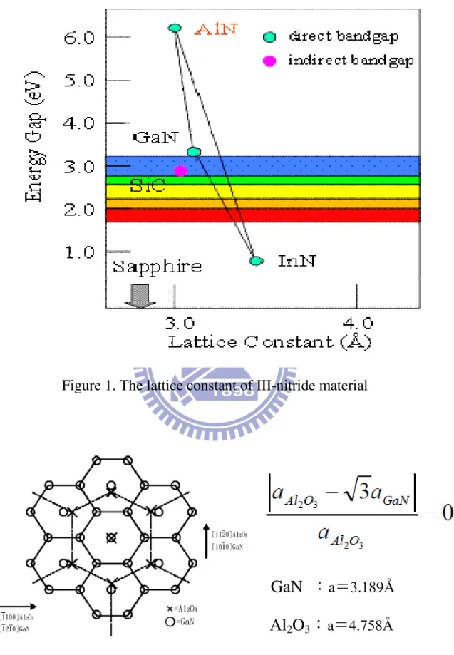
However, the development was not successfully. Because the lattice constant between GaN and sapphire substrate has a large mismatch about 16%. That will cause the high density of dislocation and limit the high quality GaN crystallize [2]. The physical character of sapphire and III-nitride showed in Table 1. and Table 2. The lattice constant showed in Figure 1. The GaN unit cell(0001) grew on sapphire(0001) has spin 30。
degree and the lattice mismatch calculate formula showed in Figure 2.
Until 1983, the Yashida, he grown a AlN buffer ( nucleation layer ) on sapphire substrate first by Molecular beam epitaxial ( MBE ). Then grew GaN film on AlN buffer that obtained better quality GaN [3]. Later the Akasaki use the Metal Organic Chemical Vapor Deposition (MOCVD) to grow AlN buffer in low temperature about 600 . Then grown the GaN film ℃ in high temperature about 1000 [4]. In 1991, Nakamura changed the AlN ℃ buffer to GaN buffer in low growth temperature, and high temperature grown GaN film [5]. It obtained the high quality GaN film too. The purpose of the AlN buffer growth defined by I. Akasaki in 1989 [6]. The comparison
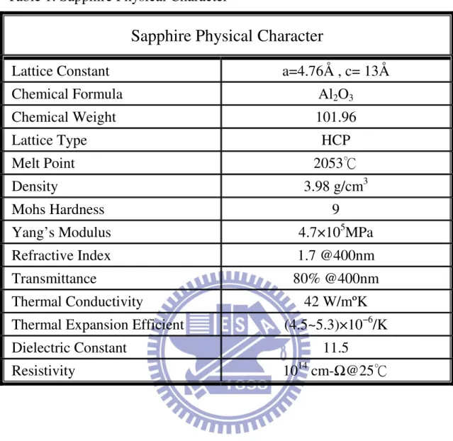
Sapphire Physical Character
Lattice Constant a=4.76Å , c= 13Å
Chemical Formula Al2O3 Chemical Weight 101.96 Lattice Type HCP Melt Point 2053℃ Density 3.98 g/cm3 Mohs Hardness 9
Yang’s Modulus 4.7×10⁵MPa
Refractive Index 1.7 @400nm
Transmittance 80% @400nm
Thermal Conductivity 42 W/mºK
Thermal Expansion Efficient (4.5~5.3)×10−6/K
Dielectric Constant 11.5
Resistivity 1014 cm-Ω@25℃
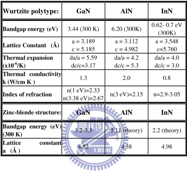
Wurtzite polytype:
GaN
AlN
InN
Bandgap energy (eV) 3.44 (300 K) 6.20 (300K) 0.62- 0.7 eV(300K) Lattice Constant (Å) a = 3.189 c = 5.185 a = 3.112 c = 4.982 a = 3.548 c=5.760 Thermal expansion
(x10-6/K) da/a = 5.59 dc/c=3.17 da/a = 4.2 dc/c = 5.3 da/a = 4.0 dc/c = 3.0
Thermal conductivity
k (W/cm K ) 1.3 2.0 0.8
Index of refraction n(1 eV)=2.33
n(3.38 eV)=2.67 n(3 eV)=2.15 n=2.9-3.05 Zinc-blende structure:
GaN
AlN
InN
Bandgap energy (eV)(300 K) 3.2-3.3 5.11 (theory) 2.2 (theory) Lattice constant
a (Å ) 4.52 4.38 4.98
Figure 1. The lattice constant of III-nitride material
Figure 2. The lattice mismatch between GaN and sapphire
GaN :
a=3.189ÅAl
2O
3:
a=4.758Å(a)The GaN growth within AlN buffer
1.2 Epitaxial Lateral Over Growth ( ELOG )
[7]
The buffer will release the lattice mismatch and various thermal expansions between sapphire and GaN. That will decrease the thread dislocation density ( TDs ) to 108 cm-2 . However, for the reason of high power applications, the TDs must decreased under 108cm-2. In 1994, the Kato et al. announced the selective area epitaxy ( SAE ) to grow the GaN on sapphire. They coated a SiN film on the GaN normally growth. Then formed patterns on SiN film and regrown GaN. The GaN composition only grown on the GaN among the SiN breach. Base on SAE, in 1997, the Nakamura used the Epitaxial lateral overgrowth ( ELOG ) to grow GaN and reduce the TDs successfully.
The ELOG growth model according to the Figure 4. :
(1) Grow a GaN on sapphire(2) Coat a SiN or SiO2 on GaN
(3) Etch the coating then remain stripe pattern
(4) Continence grow GaN on the pattern with high temperature (5) The GaN will grow laterally and close become to a complete
film
(1) (2) (3)
(4) (5)
1.3 Pattern Sapphire Substrate ( PSS )
Depending of the ELOG, the lateral growth mechanism could reduce the TDs usefully. In 2001, K. Tadatomo et. al. of the Mitsubishi Cable & Yamaguchi U. , Japan, reported a new technique that “Epitaxy growth on periodic Pattern Sapphire Substrate”[8]. They used Dry-etching technique to fabricate the periodic stripe patterns sapphire substrate. Then grow the GaN base UV LED on PSS( figure 5 ) and Flip-Chip process to obtained the low TDs and over 5 times of external quantum efficiency enhancement. The growth model showed in figure 6. After that, several groups continually reported the studies of the PSS and obtained the excellent performances. Some of the studies list in Table 3. [8]~[33].
(1) Nucleation
(2) Grains growth
(3) Coalescence
(4) Crystallize
Figure 6. The PSS growth modelAuthor/Year
Methods
Performance
K. Tadatomo / 2001 Dry-etching Stripe Output power 15.6 mw M. Yamada / 2002 Dry-etching Honey nest + flip-chip Output power 35.5% enhance Y.K. Su / 2003 Dry-etching Stripe Output power 36% enhance Y.K. Su / 2004 Dry-etching Stripe Output power 25% enhance K.M Lau / 2004 Dry-etching Stripe EL intensity 21%enhance H.C. Kuo / 2005 Dry-etching Stripe Output power 20% enhance D.S. Wuu / 2005 Dry-etching Hole Output power 21% enhance D.S Wuu / 2005 Dry-etching Hole EL intensity 23% enhance H.C. Kuo / 2006 Wet-etching Hole EQE 16.4% increase
H.C. Kuo / 2006 Wet-etching Hole Output power 40% enhance D.S. Wuu / 2006 Wet-etching Hole + ELOG Output power 30% enhance D.S. Wuu / 2006 Wet-etching Hole Output power 25% enhance D.S. Wuu / 2006 Dry-etching Hole Output power 39% enhance D.S. Wuu / 2006 Dry-etching Hole Output power 59% enhance D.S. Wuu / 2007 Dry-etching Hole Output power 35% enhance Y.K. Su / 2007 Dry-etching Cylinder Output power 50% enhance C.F Shen / 2007 Dry-etching Cylinder Output power 53% enhance H.C. Kuo / 2007 Dry-etching Cylinder Output power 65% enhance T.V. Cuong / 2007 Wet-etching Stripe Output power 160% enhance T.V. Cuong / 2007 Wet-etching Triangle Output power 100% enhance J.H. Lee / 2007 Dry-etching Hemisphere Output power 35% enhance D.S. Wuu / 2008 Dry-etching Stripe Output power 35% enhance H. Gao / 2008 Wet-etching micro Triangle Output power 29% enhance H. Gao / 2008 Wet-etching nano Triangle Output power 48% enhance
1.4 The Principle of GaN Growth on PSS
The shapes of PSS usually demonstrated the strip, hole, column, lens, cone, and pyramidal type. These PSS techniques had been proved for enhance the GaN LED output power. The PSS fabricated sort 2 mechanisms approximately: Dry-Etching and Wet-Etching. The different etching method was employ plasma or chemical solution. The PSS process shows figure 7.
(a) Photo resister coating on sapphire
(b) Photo Lithography
(c) Etching
(d) Remove PR
The Dry-Etching method formed the pattern accurately. Recently, more and more reports indicate the lens or cone shape pattern have better performance of light extraction efficient. In 2007, J.-C. Song et al. published the paper of GaN growth on lens-shape pattern and the GaN epitaxy state[34]. The GaN epitaxy state showed in Figure 8. Then in 2008, T. S. OH
et al. measured the cathode luminescence (CL) on pattern and flat regions,
respectively[35]. The data showed in Figure 9. These studies proved the epitaxy state of growth on PSS was similar the ELOG. The GaN epi layer will lateral growth and coalescence on the top of patterns. Therefore the technique of PSS beside enhanced the light extraction, it also reduced the TDs.
Figure 8. The SEM of GaN growth on PSS[34]
SEM images of a GaN on PSS for growth time (a) 10 min, (b) 20 min, (c) 30 min, (d) 40 min and (e) 80 min
Figure 9. The comparison of CL and SEM for GaN growth on PSS[35]
(a) and (b) Monochromatic top view CL image of LED grown on ML-PSS. Dotted circles indicate ML-pattern regions.(c) Integrated CL spectra for bright and dark region on the LED surface at room temperature. A and B indicate the flat regions and ML-patterned regions, respectively.
1.5 The Wet-Etching Method of PSS Fabrication
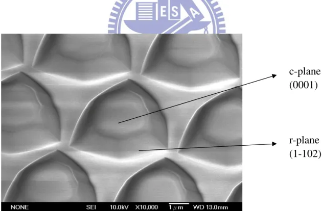
Compared with the Dry-etching PSS, the Wet-etching provided the advance fabrication technique. In the Dry-etching fabrication, the sapphire surface was be damaged unavoidably during the Dry-etching. The damaged surface would increase the difficulty while epitaxy. Otherwise, the Wet-etching would cause the particular crystallography-etched facet with an inclined slope about 45° and 57°[36]( Figure 10.). Refer to the Rhombohedral structure and surface planes of sapphire[37][38] ( Figure 11.). The particular slant was defined the r-plane(1-102)[39]. Many groups had prove the slants would enhance the light extraction efficiency usefully.
Figure 10. The SEM image of Wet-etching PSS
c-plane (0001)
r-plane (1-102)
The Wet-etching PSS fabricate process usually employed the mixture solution of H3PO4 and H2SO4 with the ratio of 5 to 2 in 240 to ℃
300 [℃ 40]. The fabricated procedure was similar the Dry-etching. But no matter what shape of the mask in photo lithography process, the etching pattern always obtained the r-plane facet. Furthermore, the pattern as etching time increase as become triangle-shape of the flat c-pane(0001). Finally the c-plane disappeared and only remained r-plane(1-102) showed in Figure 12. The r-plane(1-102) demonstration showed in Figure 13.
Figure 11. The structure of sapphire[37][38] ˙:Al
Figure 12. The etching time of sapphire Wet-etching[41] (a) 1’40” (b) 3’30” (c) 5’20” (d) 7’10”
1.6 The Predicament of Wet-etching PSS
However, the Wet-etching technique provided excellent performances of GaN LED development. The slants(r-plane) of sapphire enhanced the light extraction. But also raise the difficult of epitaxy on PSS. Normally, the GaN epilayer will grow on c-plane(0001) of sapphire. But in epitaxy on Wet-etching PSS, the GaN epilayer will also grow on r-plane(1-102). Thereforer we could obtain 2 orientation crystals of the GaN growth on Wet-etching PSS[42]. According to the Figure 14. The 2 different orientations of GaN crystals, GaN I and GaN II observed in the cross-section TEM image. The growth schematic showed in Figure 15. Though the GaN epilayer growth on r-plane will reduce the dilocation density, but the GaN grains growth on c-plane and r-plane won’t coalesence among the different grains[43]. Futhermore the bondary among the different grains existed many thread dislocations extended to the GaN surface as figure 16.
Figure 14. Cross-sectional TEM image of GaN grown on stripe Wet-etching PSS [42]
(a) Bright-field TEM image of GaN grown on stripe-patterned sapphire substrate.
(b) Enlarged image of side etching faces of sapphire striped mesa.
(c) Bright-field image of one complete GaN stripe and schematic representation of orientation relationship among GaN I, GaN II, and sapphire substrate.
(d) and (e) SAD patterns taken from the interface region between sapphire and GaN I and between sapphire GaN II
Figure 15. Schematic of the GaN growth on Wet-etching PSS [42]
Figure 16. SEM image of GaN growth on Wet-etching PSS [43]
There was undulation on the GaN surface in figure (a). In the magnified title-view could observe the split GaN I and GaN II obvious.
The dislocations extended to surface were the major reason of leakage current for the GaN LED. Beside, the dislocations will also reduce the capability for against ESD (Electro Static Discharge) seriously. Therefore the GaN growth on r-plane would cause more difficult of epitaxy on Wet-etching PSS even though that could provide high light extraction efficiency and low fabrication coast. There is only few LED manufacturer employ the Wet-etching PSS. The yield is the great issue.
In this thesis, we try to avoid the GaN growth on r-plane in epitaxy and fabricate high quality GaN LED growth on Wet-etching PSS.
Chapter 2
Experiment Purpose and Design
In this thesis, we employed the MOCVD ( Metalorganic Chemical Vapor Deposition ) to demonstrate the experiments. The MOCVD is the major technique for fabricate GaN base LED. The MO sources include TMGa ( Trimethylgallium )、TMAl ( Trimethylaluminum )、TMIn
( Trimethylindium )、Cp2Mg (Biscyclopentadienyl-Magnesium ) and NH3
( Ammonia )、 SiH4 ( Silane ) for hydride sources. The Wet-etching PSS was
fabricated by the mixture solution of H3PO4 and H2SO4 with the ratio of 5 to
2 in 270℃ for 12 mins. The shape and dimension of the patterns are popular specifications as 2 x 1.5 x 1.5 ( µm ) as indicating in figure 17.
Figure 17. The dimension of the patterns on Wet-etching PSS
Shape:::: Triangle pyramidal
Diameter::::2µm
Pitch::::1.5µm
2.1 The Experiment Principle
There were few reports or discussions relate the GaN growth condition of Wet-etching PSS by epitaxy before. And not to mention about how to avoid the GaN epilayer growth on r-plane. Therefore the past reports had no much reference in public information.
In 1991, the K. Hiromatsu defined the procedure of the GaN growth on sapphire for the purpose of AlN buffer[44]. The procedure include :
( 1 ) AlN growth formed Columnar in low temperature ( 2 ) GaN growth nucleated in high temperature
( 3 ) GaN film growth continued
( 4 ) GaN growth formed the island shape ( 5 ) GaN lateral growth
( 6 ) Coalescence
The procedure showed in figure 18. The GaN would be formed the columns in low growth temperature because the GaN didn’t has enough crystallize energy. The GaN columns only grew up vertically but not coalescent. Therefore the GaN won’t form a large superficial of film and the flat surface. In the same year, S. Nakamura employed the GaN buffer to replace AlN buffer and proved the GaN buffer possessed the higher performace than AlN buffer[45].
The other side, the study of GaN grown on Si(111) substrate, that employed a low growth temperature AlN inserted the interface between the GaN and Si substrate[46]. Because the LT-AlN had lots pits that will lead the
Therefore, we supposed the same mechanisms should also suit the GaN growth on Wet-etching PSS. The critical point is to prevent the GaN formed the large dimension grains by low growth temperature. The difference compare to conventional epitaxy is persisting the low growth temperature to grow GaN columns until cover the pattern completely. Than increase the growth temperature to cause the GaN lateral growth over the patterns and form a flat film finally. The GaN growth in low temperature perhaps grew become the polymer even amorphous. There are most exist a lot of defects in GaN. The defects will release the stress between GaN and sapphire. Then increases the growth temperature, the LT-GaN will be recovered by lateral growth in high temperature. Though the LT-GaN was poor but that would improve during heating to high temperature[47]. The recover temperature demonstrated about 1000℃[48]. Finally, grows n-GaN in the high temperature and accomplishes the LED structure. The LT-GaN growth mechanism lists below and sketches as figure 19.
(1) Buffer growth
(2) GaN growth in Low Temperature (3) GaN Columnar growth
(4) GaN island growth in High Temperature (5) GaN Lateral growth
1.
(1)Buffer growth
2.
(2)GaN growth in Low Temperature
3.
(3)GaN Column growth
4.
(4)GaN island growth in High
Temperature
5.
(5)GaN Lateral growth
6.
(6)Coalescence
2.2 The Normal GaN LED Structure
The generally, GaN LED has the basic structures : (1)Buffer layer (2) u-GaN (3) n-GaN (4) MQW (5) p-AlGaN (6) p-GaN. Recently, most research groups will insert a CART ( Charge Asymmetric Resonance Tunneling ) that composed by InxGa1-xN or GaN/InxGa1-xN Super lattice
before the MQW[49][50]. The CART structure could reduce the forward voltage, relaxed the QW stress, and enhance output power. The general sketch of CART GaN LED structure showed in figure 20. In this thesis, the purpose is grow the GaN on Wet-etching PSS. Therefore we employed the same structure of GaN LED for all the samples. The sketch and growth conditions as showed in figure 21. and table 4. The u-GaN divided 2 stages of roughing and recover layer. The roughing layer is low temperature grow and the recover layer is high temperature grow in definition. The durations of roughing and recover are 60 minutes and 30 minutes respectively and illustrated by reflectance of surface as figure 22. The reflectance was provided by MOCVD for mornited the epilayer thickness during epitaxy.
Parameters Parameters Parameters Parameters Layer Layer Layer Layer Growth Temperature Growth Temperature Growth Temperature Growth Temperature ((((℃℃℃℃)))) Growth Pressure Growth Pressure Growth Pressure Growth Pressure (mbar) (mbar) (mbar)
(mbar) ThicknessThicknessThicknessThickness ( ( ( (ÅÅÅÅ)))) Contact Layer
Contact Layer Contact Layer
Contact Layer p+GaNp+GaNp+GaNp+GaN 750 200 200
pppp----GaNGaNGaNGaN 1000 100 2500
pppp----AlGaNAlGaNAlGaNAlGaN 950 100 300
InGaN InGaN InGaN InGaN 750 200 30 QW QW QW
QW x 6 pairs x 6 pairs x 6 pairs x 6 pairs
GaN GaN GaN GaN 850 200 120 CART CART CART
CART InGaNInGaNInGaNInGaN 900 200 600
nnnn----GaNGaNGaNGaN 1060 200 25000
Recover Recover Recover
Recover 1060106010601060
uuuu----GaNGaNGaNGaN
Roughing Roughing Roughing Roughing 1030103010301030 300 15000 Buffer Buffer Buffer Buffer 530 500 200 1. Buffer 200Å 2. u-GaN 1.5 μm 3. n-GaN 2.5 μm 4. CART 5. MQW 6 pairs 6. p-AlGaN 7. p-GaN 2500Å 8. p+GaN
Figure 21. The sketch of GaN LED structure
2.3 The Experiment Design
Base on the normal GaN LED, we try to employ low temperature to grow the GaN recover layer. Therefore we fixed the growth parameters but the growth temperature of roughing layer. Adjust the growth temperature to 1030℃℃ 、℃℃、、、1000℃、、、、970℃、、、、and 940℃respectively for 4 experiments.
Furthermore, increased the recover layer thickness to 3 µm for fully cover the patterns. The other growth parameters would fix as possible as the normal GaN LED(Table 4.) and finish the GaN LED epitaxy. The growth parameters of 4 experiments were list in table 5.
• Buffer Layer
Temperature:530℃ Thickness :200Å
• Roughing / Recover / u-GaN Layer Temperature:1030 =>1060 ℃ Thickness :1.5 μm •n-GaN Temperature:1060 ℃ Thickness :2.5 μm • HT Clean Temperature:1080℃ 5 min. Recover Layer Roughing Recover u-GaN n-GaN Buffer Wafer Temp. HT Clean
• Buffer Layer
Temperature:530℃ Thickness :200Å
• Roughing / Recover /u-GaN Layer Temperature:1030 =>1060 ℃ Thickness :1.5 μm • n-GaN Temperature:1060 ℃ Thickness :2.5 μm • HT Clean Temperature:1080℃ 5 min.
• Roughing / Recover Layer Temperature:1000 =>1060 ℃ Thickness :3 μm
• Roughing / Recover Layer Temperature:970 =>1060 ℃ Thickness :3 μm
• Roughing / Recover Layer Temperature:940 =>1060 ℃ Thickness :3 μm
Experiment 2.
Experiment 3.
Experiment 4.
• Roughing / Recover Layer Temperature:1030 =>1060 ℃ Thickness :3 μm
Experiment 1.
Table 5. The Experiment parameters
Chapter 3
Experiment Result and Analysis
In this chapter, we characterized the 4 samples with OM ( Optical Microscope ), X-RD ( X-Ray deffractometer ), SEM ( Scanning Electron Microscope ), EL ( Electro Luminescence ), TEM ( Transmission Electron Microscope ), IS ( Integrating Sphere ) , etc. to verify the optical and electrical characteristic and proved the optimum growth condition for GaN growth on Wet-etching PSS. Furthermore, we also febricated the Dry-etch PSS LED and conventional GaN LED with the same structure for contrasted.
Referred to the reflectance curve by MOCVD. The reflectance indicated the smoothness of the film surface. The figure 23. and figure 24. showed the reflectance of sample 1 and sample 4 respectively. The major difference between 2 figures was the reflectance curve during u-GaN growth. The reflectance kept fluctuated and higher in figure 23. But in figure 24, the reflectance was dropped to minimum then raised up. That we supposed the GaN film became 2-Dimension growth while the temperature higher than 1000℃[48], and until to n-GaN growth. The other side, there was the second recover layer during u-GaN growth in figure 24. That meant the GaN epilayer passed through 3-Dimension growth in low temperature, then became 2-Dimension growth in high temperature. Supposed the low reflectance duration indicated the GaN had fully cover the pattern on sapphire and the GaN Columns began lateral growth. The reflectance raised duration indicated the GaN islands had coalescence.
Figure 23. The Reflectance of GaN growth in 1030℃
Figure 24. The Reflectance of GaN growth in 940℃
Recover Layer Roughing Recover u-GaN n-GaN Buffer Wafer Temp. Reflectance HT Clean Recover Layer Roughing Recover u-GaN n-GaN Buffer Wafer Temp. Reflectance HT Clean 2nd Recover
3.1 OM Morphology
The surface of the GaN LED is a simple estimate indication for the epilayer quality. There would observe the v-shape pits obvious if the GaN LED had a poor crystallization, especially in GaN growth on Wet-etching PSS. The pits are usually large and visibly. The figure 25. showed the surface morphologies of the sample 1. by OM. The magnification is 1000x and focused at patterns and surface of the sample. There would observe lots of pits on the surface in figure 25(a). The figure 25(b) and 25(c) were the same position as the 25(a) but focus at middle and bottom of epilayer respectively. That illustrated the pits always appeared at the apex of the triangle patterns. The figure 26. was the comparison of the surface mophology of 4 samples. That observed the sample 1 had more pits than sample 2. The sample 3 and sample 4 were not.
(a) Focus at surface
(b) Focus at middle
(c) Focus at bottom
Sample 1. 1030℃
Sample 2. 1000℃
Sample 3. 970℃
3.2 X-RD Analysis
The X-Ray deffractometer could verify the quality of the crystallization[51]. Usually depend on the full-widths at half-maximum (FWHM) of (102) plane measurement. The X-RD comparison and the FWHM f (102) plane showed as figure 27. The X-RD FWHM of ( 102 ) plane were 500.38, 432.85, 413.39, and 358.25 for sample 1 to sample 4 respectively. The FWHM of conventional GaN LED and Dry-etch PSS are 415.15 and 372.44 respectively. The narrow FWHM usually indicated the crystal quality was better.
0 1000 2000 3000 4000 5000 23.7 23.8 23.9 24 24.1 24.2 24.3 24.4 24.5 Sample 1 1030℃ FWHM : 500.38 Sample 2 1000℃ FWHM : 432.85 Sample 3 970℃ FWHM : 413.39 Sample 4 940℃ FWHM : 358.25 Dry-etch PSS FWHM : 372.44 Conventinal FWHM : 415.15
3.3 SEM images
The SEM image would provide the more accurate morphology and dimension measurement of surface or cross section. The figure 28. was the cross section image of GaN LED growth on the Dry-etching PSS. The difference of pattern size is because the cross section cutting position. There had not obviously irregular GaN crystal growth arround the pattern. The figure 29. showed the SEM images of the samples. There were lots defects obvious on surface and cross section of sample 1 and sample 2. The sample 3 and sample 4 were not.
Figure 28. The SEM images of GaN LED growth on the Dry-etching PSS
Figure 29. The SEM images of samples Sample 1 1030℃
Sample 2 1000℃
Sample 3 970℃
3.4 EL Data
The samples formed the chip before EL measured. The chip process included n-GaN mesa etching, 2500Å thick ITO coated on p+GaN for transparent contact layer, and 2 µm thick Cr/Pt/Au metal deposited on ITO and exposed n-GaN for electrodes. Then back polished to total thickness of wafer about 90 µm and cut the chip size to 10 x 23 mil as figure 30. The EL test parameters for optical character, leakage current, reverse voltage were 20 mA, -8 v and -10 μA respectively. The ESD test parameters were from -1000 v to -8000 v and measured -1000 v per step with human body mode(HBM). The EL measurements and test parameters listed in table 6. The comparison of forward voltage showed in figure 31. The comparison of ESD and Ir showed in figure 32.That had a obvious variation in ESD and Ir ability. The Vf, Ir, Vz, and ESD of conventional GaN LED were 3.23 v, 0.012μA, 20 v, and 6432 v respectively. Those accorded the normal GaN LED specifications. Therefore the GaN LED structure employed in this experiment was referable. Both the optical and electrical characteristic of sample 4 had approch to the Dry-etchng PSS but other samples not.
10 mil 23 mil
LOP1
LOP1
LOP1
LOP1 WLD1
WLD1
WLD1 WLP1
WLD1
WLP1
WLP1
WLP1 VF1
VF1
VF1 HW1
VF1
HW1 Ir
HW1
HW1
Ir
Ir
Ir
VZ1
VZ1
VZ1
VZ1
20mA 20mA 20mA 20mA 20mA -8v -10µA
Sample 1 Sample 1 Sample 1 Sample 1 - 1030℃ - 1030℃ - 1030℃ - 1030℃ 543 6.2% 11.1% 108.8 452.1 447.1 3.21 22.9 0.134 16.6 Sample 2 Sample 2 Sample 2 Sample 2 - 1000℃- 1000℃- 1000℃- 1000℃ 489 10.6% 23.4% 116.3 452.6 447.1 3.18 22.6 0.059 16.3 Sample 3 Sample 3 Sample 3 Sample 3 - 970℃- 970℃- 970℃- 970℃ 3943 65.5% 74.7% 125.6 453.4 448.1 3.23 20.7 0.032 19.7 Sample 4 Sample 4 Sample 4 Sample 4 - 940℃- 940℃- 940℃- 940℃ 6531 81.5% 82.7% 114.8 450.0 444.6 3.21 20.7 0.011 20.0 Dry-etching PSS Dry-etching PSS Dry-etching PSS Dry-etching PSS 6448 82.9% 83.2% 120.2 451.8 445.6 3.23 20.6 0.009 19.7 Convventional Convventional Convventional Convventional 6432 81.6% 81.9% 72.4 447.8 441.9 3.23 20.1 0.012 20.0 Wafer No Wafer No Wafer No Wafer No
HBM ESD(w/o IR fail)
Chip form prob measurement
Chip form prob measurement
Chip form prob measurement
Chip form prob measurement
AVG >2000 >1000 VF1 VF1 VF1 VF1 3.15 3.16 3.17 3.18 3.19 3.20 3.21 3.22 3.23 3.24 Sample 1 -1030℃ Sample 2 -1000℃ Sample 3 - 970℃ Sample 4 - 940℃ Dry-etching PSS Convventional V
Table 6. The EL measurement
Leakage Current Leakage CurrentLeakage Current Leakage Current 0.000 0.020 0.040 0.060 0.080 0.100 0.120 0.140 0.160 Sample 1 -1030℃ Sample 2 -1000℃ Sample 3 - 970℃ Sample 4 - 940℃ Dry-etching PSS Convventional μA HBM ESD(w/o IR fail) HBM ESD(w/o IR fail)HBM ESD(w/o IR fail) HBM ESD(w/o IR fail) 0 1000 2000 3000 4000 5000 6000 7000 Sample 1 -1030℃ Sample 2 -1000℃ Sample 3 - 970℃ Sample 4 - 940℃ Dry-etching PSS Convventional V
3.5 TEM images
The TEM image that would verify the GaN crystal quality and analyze the material structure. Refer to the reports past indication. The GaN growth on r-plane was zinc blende structure ( figure 33 ) [52]. The GaN II was observed from r-plane as figure 33 (a) – d. Used selected area diffraction ( SAD ) analyzed the region figure 33 (a) – c to f and obtained the images figure 33 (c) to (f). The normal GaN was wurtzite structure as figure 33(c). Zinc blende structure GaN showed in figure 33(d). The sapphire showed in figure 33(e). The zinc blende GaN was only observed along the r-plane of sapphire.
The figure 34 is the TEM and SAD image of the sample 4. There was no obviously different crystal between GaN and sapphire. The SAD analysis indicated the GaN in 1 and 3 regions were both the same orientation of wurtzite structure.
5977.37 nm
1
2
3
3.6 IS measurement
The output power and efficiency droop of LED device was measured by IS system. The samples need mount on Ag-TO first. Control the input power from low current to high current and measure the output power each step. The output power reduction at high injection current could determine the behavior of device. Recently, the efficiency droop was discussed more and more in LED illumination market. The cause of the efficiency droop proposed including Auger recombination, junction heating, polarization field, carrier leakage, and defect [53]. Therefore the dislocation density is also the one of the efficiency droop causes. The IS tend diagrams of the output power, Wall-Plug Efficiency(WPE), and Extraction Quantum Efficiency(EQE) drew in figure 35, figurer 36, and figure 37 respectively. The Output Power at 20 mA measurement listed in table 7. In the measurement, the sample 4 has both the higher output power and WPE. Especially in high injection current, as the figure 35(b), figure 36(b), and figure 37(b). That meant the sample 4 has better crystal quality than others. Furthermore, the figure 38(a), (b), and (c) showed the comparison of sample 4, Dry-etching PSS, and conventional GaN of output power, WPE, and EQE curve respectively. The result of sample 4 was similar to Dry-etching PSS and the output power was 1.27 times enhance than conventional GaN LED. That showed the behaviors of sample 4 had approach to Dry-etching PSS LED and better than other samples.
Output Power
0 20 40 60 80 100 120 140 0 50 100 150 200 250 300 350 400 450 mA mW Sample1-1030℃ Sample2-1000℃ Sample3-970℃ Sample4-940℃Output Power
80 85 90 95 100 105 110 115 120 125 130 150 170 190 210 230 250 270 290 mA mW Sample1-1030℃ Sample2-1000℃ Sample3-970℃ Sample4-940℃ (a) (b)WPE
0% 5% 10% 15% 20% 25% 30% 35% 40% 0 50 100 150 200 250 300 350 400 mA mA mA mASample1-1030℃
Sample2-1000℃
Sample3-970℃
Sample4-940℃
WPE
3% 4% 5% 6% 7% 8% 9% 10% 11% 12% 200 220 240 260 280 300 mA mA mA mASample1-1030℃
Sample2-1000℃
Sample3-970℃
Sample4-940℃
Figure 36. The WPE measurement comparison (b)
EQE
0% 5% 10% 15% 20% 25% 30% 35% 40% 0 50 100 150 200 250 300 350 400 mA mA mA mASample1-1030℃
Sample2-1000℃
Sample3-970℃
Sample4-940℃
EQE
20% 22% 24% 26% 28% 30% 32% 34% 36% 38% 40% 0 20 40 60 80 100 120 mA mAmA mASample1-1030℃
Sample2-1000℃
Sample3-970℃
Sample4-940℃
(a) (b)NO. Wd(nm) If (mA) Vf(v) If (mA) OP ( mW ) WPE EQE Sample 1 - 1030℃℃℃℃ 455 20 3.18 20 15.89 24.98% 29.14% Sample 2 - 1000℃℃℃℃ 450 20 3.17 20 18.17 28.67% 33.00% Sample 3 - 970℃℃℃℃ 455 20 3.18 20 18.31 28.82% 33.60% Sample 4 - 940℃℃℃℃ 451 20 3.16 20 19.05 30.13% 34.69% Dry-etching PSS 452 20 3.18 20 19.23 30.26% 35.09% Conventional 449 20 3.20 20 15.02 23.47% 27.23%
Table 7. The Output Power at 20 mA measurement
Output Power 0 20 40 60 80 100 120 140 0 100 200 300 400 mA mW Sample4-940℃ Dry-etching PSS Conventional WPE 0% 5% 10% 15% 20% 25% 30% 35% 40% 0 50 100 150 200 250 300 350 400 m A m A m A m A Sample4-940℃ Dry-etching PSS Conventional EQE 0% 5% 10% 15% 20% 25% 30% 35% 40% 0 50 100 150 200 250 300 350 400 m A m A m A m A Sample4-940℃ Dry-etching PSS Conventional
3.7 Etching-Pits Density
The etching-pits density is an other way to verify the structure quality. The sample fabrication was etched by H3PO4 in 240 for 2 minutes.℃
Than observed the surface morphology by SEM. The SEM image of sample 4 was shown in figure 39. But there were not obviously etching-pits on the surface. However, the side-wall of the device had the bevel angle etching shape. That perphaps meant the interface between low growth temperature GaN and sapphire was etched easier than high growth temperature GaN.
10000 X 200 X
5000 X
10000 X 5000 X
Chapter 4
Conclusions and Future Work
In this thesis, w e tried to avoid the GaN crystal growth on r-plane of Wet-etching PSS by modify epitaxy condition. In the experiment, we decreased the recover layer GaN growth temperature for expected the GaN grew become large grains. Than increased the growth temperature to cause the epilayer growth laterally and coalescence. Finally, compared the characters of samples and proved the optimum epitaxy parameters. We also compared the behaviors of Dry-etching PSS and conventional GaN to confirm the improvement was not due to the LED structure over u-GaN.
4.1 Results discussion
Refer to the Chapter 3, we compared the surface morphology of 4 samples. There were lots pits on the surface of sample 1 and 2 ( figure 24 ). But the sample 3 and 4 were not. The observation of cross section by SEM was proved the sample 1 and 2 had more defects existed between GaN and sapphire ( figure 27 ). The sample 3 seemed also has the unobvious defects in the SEM image. The sample 4 was no visible pit in either of OM and SEM images. The X-RD FWHM of ( 102 ) plane were 500.38, 432.85, 413.39, and 358.25 for sample 1 to sample 4 respectively ( figure 25 ). In electronic characterization, the leakage current were 0.134 µA, 0.059 µA, 0.032 µA, and 0.011 µA at -8 v for sample 1 to sample 4 respectively ( figure 29 ). The ESD average value were 543 v, 489 v, 3943 v, and 6531 v, the yield over -2000 v were 6.2 %, 10.6 %, 65.5 %, and 81.5 % respectively. The leakage current and ESD behaviors indicated the performance of the
structure quality. The output power were 15.89 mw, 18.17 mw, 18.31 mw, and 19.05 mw at 20mA for sample 1 to sample 4 respectively ( Tabe 7. ). But the output power were the almost the same level at low injection current. That perhaps related to the junction heating cause the recombination efficiency reducing. Otherwise, the observation of the TEM image for sample 4, there were not different crystal between GaN and sapphire ( figure 31 ). And the SAD analysis indicated the GaN epilayer was complete wurtzite structure.
Summarize the analysis above we could determine the sample 4 had the better structure quality than others. Furthermore, there had not irregular GaN crystal growth on r-plane of Wet-etching PSS in observation. Compared to the Dry-etching PSS and conventional GaN LED with sample 4, the electrical characteristics were all the same level in Electro Luminescence test. Therefore the method of the epitaxy recover layer GaN growth in low temperature would avoid GaN crystal growth on r-plane of Wet-etching PSS and wouldn’t reduce the structure quality.
4.2 Future Work
The Wet-etching PSS for GaN LED is advantageous to production. But the GaN on r-plane will reduce the yield of device. That’s the major reason for most corporations didn’t employ the Wet-etching PSS. Even though the Wet-etching PSS has the excellent performance. We expect thesis would provide the some contribution for GaN LED fabricate technique. However, the last report indicated the output power of GaN LED had
a great gap to us. We still need more efforts.
Suppose the method of low temperature grow GaN should not only suit growth on Wet-etching PSS. That should suit apply to growth on any lattice mismatch substrate such as Si, SiC, etc. The growth temperature probably related to the variation of material. And the recover layer duration should as increase as growth temperature reduce. The otherwise, due to the bevel angle etching pattern under epilayer in figure 33. That perphaps meant the low growth temperature GaN was etched easier than high growth temperature GaN. The effect maybe contributes the side-wall etching process or the chemical GaN lift-off.
References
[1] J. I. Pankove et al. “Electoluminescence in GaN” J. Luminescence, 4, 63, 1971
[2] S. D. Lester et al. “High dislocation densities in high efficiency GaN-based light-emitting diodes,” Appl. Phys. Lett., vol. 66, pp. 1249–1251, 1995
[3] S. Yoshida, et al. “Improvements on the electric and luminescent properties of reactive molecular beam epitaxially grown GaN films by using AlN-coated sapphire substrates,” Appl. Phys. Lett., vol. 42, pp. 427–429, 1983
[4] H. Amano et al. “Metalorganic vapor phase epitaxial growth of a high quality GaN film using an AlN buffer layer,” Appl. Phys. Lett., vol. 48, pp. 353–355, 1986
[5] S. Nakamura et al. “Novel metalorganic chemical vapor deposition system for GaN growth,” Appl. Phys. Lett., vol. 58, pp. 2021–2023, 1991
[6] I. Akasaki et al. “Effects of an AlN buffer layer on crystallographic structure and on electrical and optical properties of GaN and Ga1-xAlAxN(0<x0.4)films grown on sapphire substrates by MOCVD,”
J. Cryst. Growth,, vol. 98, p. 209, 1989
[7] B. Beaumont, et al. “Epitaxial Lateral Overgrowth of GaN” phys. stat.
sol., (b) 227, No. 1, 1–43, 2001
[8] K. Tadatomo et al. “High output power InGaN ultraviolet light emitting diodes fabricated on pattern substrates using MOVPE” Jpn. J. Appl.
[9] M. Yamada, et al. “InGaN-based near-ultraviolet and blue light emitting diodes with high external quantum efficiency using a patterned sapphire substrate and a mesh electrode,” Jpn. J. Appl. Phys., Vol. 41, pp. L1431 ,2002
[10] S.J. Chang, et al. “Nitride-based LEDs fabricated on patterned sapphire substrates,” P. S. Solidi A, Vol. 47, pp. 1539, 2003
[11] Y.P. Hsua, et al. “Lateral epitaxial patterned sapphire InGaN/GaN MQW LEDs,” J. Cryst. Growth, Vol. 261, pp. 466, 2004
[12] Z.H. Feng, et al. “GaN-based blue lightemitting diodes grown, and fabricated on patterned sapphire substrates by metalorganic vapor-phase epitaxy,” J. Cryst. Growth, Vol. 272, pp. 327, 2004
[13] Y.J. Lee, et al. “Improvement in light-output efficiency of near-ultraviolet InGaNGaN LEDs fabricated on stripe patterned sapphire substrates,” Materials Science, and Engineering B-Solid State Materials
for Advanced Technology, Vol. 122, pp. 184, 2005
[14] D.S. Wuu, et al. “Enhanced output power of near-ultraviolet InGaN–GaN LEDs grown on patterned sapphire substrates,” IEEE
Photonics Technology Letters, Vol. 17, pp. 2, 2005
[15] W.K. Wang, et al. “Near-ultraviolet InGaN/GaN light-emitting diodes grown on patterned sapphire substrates,” IEEE Journal Of Quantum
Electronics, Vol. 44, pp. 2512, 2005
[16] W.K. Wang, et al. “Efficiency improvement of near-ultraviolet InGaN LEDs using patterned sapphire substrates,”IEEE Journal Of Quantum
Electronics, Vol. 41, pp. 1103, 2005
[17] Y.J. Lee, et al. “Enhancing the output power of GaN-based LEDs grown on wet-etched patterned sapphire substrates,” IEEE Photonics
Technology Letters, Vol. 18, pp. 1152, 2006
[18] Y.J. Lee, et al. “Fabrication, and characterization of GaN-based LEDs grown on chemical wetetched patterned sapphire substrates,” Journal of
the Electrochemical Society, Vol. 153, pp. G1106, 2006
[19] D.S. Wuu, et al.“Defect reduction, and efficiency improvement of near-ultraviolet emitters via laterally overgrown GaN on a GaN / patterned sapphire template,” Appl. Phys. Lett., Vol. 89, pp. 161105, 2006
[20] D.S. Wuu, et al. “Fabrication of pyramidal patterned sapphire substrates for high-efficiency InGaN-based light emitting diodes,” Journal of the
Electrochemical Society, Vol. 153, pp. G765, 2006
[21] W.K. Wang, et al. “Fabrication, and efficiency improvement of micropillar InGaN/Cu light-emitting diodes with vertical electrodes,”
Appl. Phys. Lett., Vol. 88, pp. 181113, 2006
[22] W.K. Wang, et al. “Characteristics of flip-chip InGaN-based light-emitting diodes on patterned sapphire substrates,” Jpn. J. Appl.
Phys., Vol. 45, pp. 3430, 2006
[23] R.H. Horng, et al. “Growth, and characterization of 380-nm InGaN/AlGaN LEDs grown on patterned sapphire substrates,” J. Cryst. Growth, Vol. 298, pp. 219, 2007
[24] P.C. Tsai, et al.“Lifetime tests, and junctiontemperature measurement of InGaN light-emitting diodes using patterned sapphire substrates,”
Journal of Lightwave Technology, Vol. 25, pp. 591, 2007
[26] C.E. Lee, et al. “Enhancement of flip-chip light-emitting diodes with omni-directional reflector, and textured micropillar arrays,” IEEE
Photonics Technology Letters, Vol. 19, pp. 1200, 2007
[27] H.S. Cheong, et al. “Structural, and optical properties of near-UV LEDs grown on V-grooved sapphire substrates fabricated by wet etching,” J.
Cryst. Growth, Vol. 298, pp. 699, 2007
[28] T.V. Cuong, et al. “Enhanced light output from aligned micropit InGaN-based light emitting diodes using wet-etch sapphire patterning,”
Appl. Phys. Lett., Vol. 90, pp. 131107, 2007
[29] T.S. Kim, et al. “Increase of light extraction from GaN based light emitting diodes incorporating patterned structure by colloidal lithography,” Appl. Phys. Lett., Vol. 91, pp. 171114, 2007
[30] J.H. Lee, et al. “Growth and characteristics of InGaN/GaN films grown on hemispherical patterned sapphire by using MOCVD,” The Journal of
the Korean Physical Society, Vol. 51, pp. S249, 2007
[31] W.K. Wang, et al. “Growth and characterization of InGaN-based light-emitting diodes on patterned sapphire substrates,” The Journal of
Physics, and Chemistry of Solids, Vol. 69, pp. 714, 2008
[32] H.Y. Gao, et al. “Enhancement of the light output power of InGaN/GaN lightemitting diodes grown on pyramidal patterned sapphire substrates in the micro- and nanoscale,” J. Appl. Phys., Vol. 103, pp. 014314, 2008 [33] H.Y. Gao, et al. “Fabrication of nano-patterned sapphire substrates, and
their application to the improvement of the performance of GaN-based LEDs,” Journal of Physics, Vol. 41, pp. 115106, 2008
[34] J.-C. Song et al. “Characteristics comparison between GaN epilayers grown on patterned and unpatterned sapphire substrate (0 0 0 1)” J.
Cryst. Growth, 308, 321, 2007
[35] T. S. OH et al. “GaN-Based Light-Emitting Diodes on Micro-Lens Patterned Sapphire Substrate” Jpn. J. Appl. Phys., Vol. 47, No. 7, 2008
[36] Yang Zhang et al. “High-brightness GaN-based blue LEDs grown on a wet-patterned sapphire substrate” Proc. of SPIE Vol. 6841, 68410T-2 [37] O Ambacher “Growth and applications of Group III-nitrides “J. Phys. D:
Appl. Phys., 31, 2653–2710, 1998
[38] 王偉凱, “Fabrication and characterization of Gan-based light-emitting
diodes grown on patterned sapphire substrate.”國立中興大學, 博士論
文 民國 95 年 7 月
[39] 謝奇勳, ”成長於圖案化藍寶石基板之氮化鎵發光二極體特性分析”
國立中央大學, 碩士論文 民國 96 年 7 月
[40] 潘昌吉, ” Investigation of InGaN Ultraviolet Light Emitting Diodes”
國立中央大學, 博士論文 民國 96 年 10 月
[41] 張育嘉, ”圖形化藍寶石基板應用於氮化鎵發光二極體之研究”國立
中央大學, 碩士論文 民國 97 年 7 月
[42] H. G. Chen et al. “Investigation on microstructure in GaN epitaxial growth on the stripe-patterned r-plane sapphire substrates” J. Cryst.
Growth, vol 310 1627–1631, 2008
[44] K. Hiramatsu et al. “Growth mechanism of GaN grown on sapphire with A1N buffer layer by MOVPE.” J. Cryst. Growth, vol. 115, p. 628, 1991.
[45] S. Nakamura “GaN growth using GaN buffer layer” Jpn. J. Appl. Phys., Vol. 30, No. 10A, 1991
[46] B.S. Zhang “Reduction of tensile stress in GaN grown on Si(1 1 1) by insertinga low-temperature AlN interlayer” J. Cryst. Growth, vol.270, 316–321, 2004
[47] X. H. Wu et al. “Nucleation layer evolution in metal-organic chemical vapor deposition grown GaN” Appl. Phys. Lett., 68, 1371, 1996
[48] A. Wickenden et al. “The effect of thermal annealing on GaN nucleation layers deposited on (0001) sapphire by metalorganic chemical vapor deposition”J. Appl. Phys., vol.75, 1994.
[49]Y. T. Rebane et al. “Light Emitting Diode with Change Asymmetric Resonance Tunneling” phys. stat. sol., (a) 180, 121, 2000
[50] Z. C. Feng et al. “Optical and structural properties of dual wavelength InGaN/GaN multiple quantum well light emitting diodes” Proc. of
SPIE Invited Paper Vol. 7058 70580S-12, 2008
[51] D. Keith Bowen and Brain K. Tanner, “High Resolution X-ray Diffractometry and Topography”, Page: 2, 1998
[52] Ji-Hao Cheng et al. “Improved crystal quality and performance of GaN-based light-emitting diodes by decreasing the slanted angle of patterned sapphire” Appl. Phys. Lett., 96, 051109, 2010
[53] Martin F. Schubert et al. “Effect of dislocation density on efficiency droop in GaInN/GaN light-emitting diodes” Appl. Phys. Lett., 91,
231114 , 2007
[54] Y. Narukawa et al. “White light emitting diodes with super-high luminous efficacy” J. Phys. D: Appl. Phys., 43, 354002, 2010
![Figure 5. The GaN growth on stripe PSS[8]](https://thumb-ap.123doks.com/thumbv2/9libinfo/8560566.188478/17.892.166.746.479.1038/figure-gan-growth-stripe-pss.webp)
![Table 3. PSS studies List[8]~[33]](https://thumb-ap.123doks.com/thumbv2/9libinfo/8560566.188478/19.892.135.786.173.1091/table-pss-studies-list.webp)
![Figure 8. The SEM of GaN growth on PSS[34]](https://thumb-ap.123doks.com/thumbv2/9libinfo/8560566.188478/21.892.137.759.526.928/figure-sem-gan-growth-pss.webp)
![Figure 9. The comparison of CL and SEM for GaN growth on PSS[35]](https://thumb-ap.123doks.com/thumbv2/9libinfo/8560566.188478/22.892.140.787.112.783/figure-comparison-cl-sem-gan-growth-pss.webp)