行政院國家科學委員會專題研究計畫 期中進度報告
子計畫五:DVB-T 數位視訊廣播系統之高效能數位運算核心
的設計與實現(1/2)
計畫類別: 整合型計畫 計畫編號: NSC92-2220-E-110-006- 執行期間: 92 年 08 月 01 日至 93 年 07 月 31 日 執行單位: 國立中山大學電機工程學系(所) 計畫主持人: 邱日清 計畫參與人員: 杜領彥, 林任邦, 李俊憲, 周裕良 報告類型: 完整報告 處理方式: 本計畫可公開查詢中 華 民 國 93 年 5 月 24 日
行政院國家科學委員會專題研究計畫 期中進度報告
子計畫五:DVB-T 數位視訊廣播系統之高效能數位運算核心的設計與實
現(1/2)
計畫類別: 整合型計畫 計畫編號: NSC 92-2220-E-110-006 執行期間: 92 年 08 月 01 日 至 93 年 07 月 31 日 執行單位: 國立中山大學電機工程學系(所) 計畫主持人: 邱日清 報告類型: 完整報告 處理方式: 本計畫可公開查詢中 華 民 國 93 年 5 月 17 日
目錄
目錄 ---II 中英文摘要---IV 內容 Chapter 1. DVBT_DSP Architecture ---1 1.1 VLIW ---1 1.2 Architecture Overview ---21.3 Super Element Architecture ---2
1.4 Registers ---4
Chapter 2. Addressing Mode ---7
2.1 Indirect Addressing ---7
2.2 Conditional Addressing ---8
2.3 Modulo Addressing ---9
Chapter 3. Repeat Mode ---10
Chapter 4. Instruction Set ---12
4.1 ALU Instruction ---12 4.2 Multiple Instruction ---13 4.3 Load Instruction ---15 4.4 Store Instruction ---18 4.5 Branch Instruction ---19 4.6 Repeat Instruction ---20
Chapter 5. Verification and Analysis ---21
5.1 Verification Environment ---21
5.2 Synthesis Result ---21
6.1 Implementation overview ---26
6.2 Sequential DVBT DSP assembly code generation ---28
結果與討論---37
參考文獻---38
計畫相關之著作---45
中英文摘要
一、計畫中文摘要 關鍵字: 數位訊號處理器、DVB-T、VLIW、COFDM、向量式的管道運算、FFT、 最佳化 C 語言編譯器 本計畫之主要目的在於設計與實現符合 DVB-T 數位視訊廣播系統接收器之 相關演算法運算所需之高效能數位運算核心,提供即時之資料處理以產生足夠的 訊號流的輸出。其中完成 COFDM 單元 (需即時完成 2k/8k FFT 運算)之即時運算 是本計劃最重要的關鍵。以 DSP 實現 DVB-T 系統中 COFDM 及相關演算法之 設計,其最大的好處是以軟體的方式將之實現於規律化的運算核心,簡化了大量 的資料路徑連結的問題。我們將以演算法為主軸來考慮硬體設計提供即時之資料 處理,採 VLIW 模式之向量式的管道運算結構(Vectorized Pipelining Architecture) 技術設計,此運算核心稱之為 DVBT_DSP,以產出最佳化的矽智產權,且為配 合其他子計劃的應用,本計劃除運算核心的完成外,並需設計最佳化 C 語言編譯 器設計,以配合系統整合設計之應用,以達到下列的優點: 1. 可程式的設計環境 --- 彈性化, 2. 有效率的 Cost/Performance 的考慮, 3. 高效率處理器結構 --- 前瞻性。DVBT_DSP 微架構建立了高效能的 Instruction/Data Stream buffer、
Zero-Overhead Looping( ZOL ) fetcher 和 Parallel execution data paths 等功能。若 與其他當前高效能 DSP 處理器處理 FFT 所需要的 Cycle 做比較,經評估後可達 5 倍以上的執行效能。其他子計劃將其所發展之演算法,利用本計畫所研發之整 體發展系統,轉譯成 DVBT_DSP 的可執行程式,以達成其數位訊號處理之 SOC 單元,以利總計畫之實現,且建立國內在高效能 DSP 晶片的設計基本能力與學 生的訓練培養,以協助國內產業擁有關鍵晶片的開發技術與人才。 在第一年的研究計畫中,主要目的在於 DVBT_DSP 微架構的設計。因此, 以 VLIW 模式之向量式的管道運算結構(Vectorized Pipelining Architecture) 設計為架構,並定義出高效能導向之結構的 DVBT_DSP 指令集。DVBT_DSP 的 指令集可以分成四個子集,分別是 ALU、Multiple、Load 與 Store。ALU 與 Multiple
指令集提供了並行化的乘法與 ALU 運算作業,Load 指令則支援循環儲列式的運 算結構,Store 指令值則提供零負擔的迴圈結構 (Zero-overhead Looping)。 DVBT_DSP 之指令集將會以 VLIW 之架構建立,每一個 Instruction Word 包 容有 8 = 8 個指令,每個指令長度為 16bits,因為 DVBT_DSP 可以同時處理兩個 VLIW 指令,所以指令匯流排的寬度為 256bits。
DVBT_DSP 主要是由兩個運算核心構成,此運算核心稱為 Super Element (SE)。每個 SE 的執行單元包含兩個部份,分別是 Basic Element 1(BE1)與 Basic Element 2(BE2)。BE1 以一個 16bits 算數邏輯處理器為核心,另外提供了兩個 Load 單元做 Memory read 與一個 Store 單元做 Memory write 的位址計算。BE2 則是以一個 16bits 算數邏輯處理器與 16x16bits 的乘法器為核心,另外提供了 一個 Load 單元做 Memory read 與一個 Store 單元做 Memory write 的位址計算。 整個 SE 共可提供三個 memory load、兩個 memory write 、2 個 ALU 與一個 Multiplier 的功能,在做一般運算時,BE1 與 BE2 最多可各自獨立平行處理四個 指令,資料源則來自各自的運算元。 依據 DVBT_DSP 微架構,目前已完成 DSP 核心 FPGA 硬體之設計,並於 模擬軟體與 FPGA 版上驗證指令執行無誤。目前 DVBT_DSP 主要是以數位訊號 處理常用的四個演算法(FIR、IIR、FFT 與 DCT)來做驗證,並評估處理的這些 演算法之效能。 為配合其他子計劃的應用,本年度除 DVBT_DSP 運算核心的完成外,並著 手設計 C 語言編譯器。目前完成的進度為將 C 語言轉譯成 DVBT_DSP 的機器碼。
二、計畫英文摘要
Keywords : DSP、DVB-T、VLIW、COFDM、Vectorized Pipelining、FFT、Optimized C Compiler
The main goal of this project is to design and implement the high performance processor core for completing those digital signal processing algorithms applied at the DVB-T systems to the DSP units to support the signal flow in time. In those DSP units, the COFDM unit is the key one to the real time computing, because this unit must complete the FFT algorithm at 2K and 8K input signal points. The idea to implement this unit in digital signal processors is to use the software methods instead of the hardwire methods to solve the large routing path complexity problems with the regular processing core. By the algorithm oriented design, this processing core is named as DVBTDSP. It is designed by the vectorized pipelining architecture techniques in the VLIW concepts to complete the optimal SIP and to support the DSP applications of other subprojects. In addition to complete the DVBTDSP processing core, we will design the high level language supporting in the C language extension version for the user programming interface. In this approaches to integrate the whole projects, we can get the following advantages:
(1) Programmable environments --- Flexible; (2) Efficient cost/performance tradeoff;
(3) High performance computer architecture --- Advancing.
In the DVBTDSP microarchitecture, we build the Instruction/Data Stream buffer、the Zero-Overhead Looping( ZOL ) fetcher and the parallel execution data paths. To compare with the current DSP processors, there is 5 times estimation performance advancing gotten by the DVBTDSP. Though we have been successfully designing the CPU cores, the entire project indeed sets a very challenging target for us. Nevertheless, the result of this project will significantly affect the system-level integration design of the whole project. Besides, we faithfully believe in the acquisition of fruitful experience and capability from the
development of the H/W chips, S/W simulations and high performance CPU designs. In addition, those students who are exposed to this project are believed to absorb and learn the advanced techniques and knowledge in the mentioned areas. We would like to apply for a 3-year grant from NSC for this project.
Chapter 1. DVBT_DSP Architecture
1.1 VLIW
VLIW 是一個 multiple-issue 的處理器架構,此架構的特點是使用較長(64、 128 或 256 bits)且高度並行的指令,並將這些指令均勻的分配給晶片中眾多的 執行單元來執行。在一個 VLIW 指令中,通常包含了 ALU、MUL、LOAD 與 STORE 指令,因此這些指令可以在同一個 clock cycle 執行。
使用 VLIW 架構的好處在於可以同時利用眾多獨立的執行單元來進行運 算,而缺點就是在於如何盡量使指令並行化,使執行單元能告保持忙碌的狀態。 因此,VLIW 架構的瓶頸在於指令不夠並行化,這個部份必須依靠 smart compiler 來完成。
目前已經有許多公司使用 VLIW 的架構來設計高效能的 DSP,如 TI 的 TMS320C6x 系列、Motorola 的 DSP563xx、Lucent Technologics 的 DSP16xx、 Analog Devices 的 ADSP-2116x 與 TigerSHARC 處理器。本計劃所要完成的 DVBT_DSP 也是基於 VLIW 架構所設計的 DSP。
DVBT_DSP 的 VLIW 指令配置如下,理想狀態下 DVBT_DSP 可以同時執行 兩個 ALU、一個 Multiple、三個 Load 與兩個 Store 的動作。
ALUR MUL Load1 Load2 Load3 Store1 Store2 ALUL
255 224223 192191 160159 128127 9695 6463 3231 0
1.2 Architecture Overview
DVBT_DSP 是由兩個 Super element(SE)所構成的,而每一個 Super element 都有個自的 Fetcher、Decoder、Execution Unit、Registers 與 Memory 的 Execute Unit。也就是說,一個 SE 已經是一個完整的處理核心。因此,DVBT_DSP 可說 是一個有兩個處理核心的 DSP。至於兩個處理核心 SE1 與 SE2 的溝通,則是依 靠 Shared Register 來完成這個工作。 RegisterFile Super Element Operand Dispatch Instruction Decoder Instruction Fetcher ROM RAM RegisterFile Super Element Operand Dispatch Instruction Decoder Instruction Fetcher ROM RAM Shared Registers(R16&R17) SE1 SE2 圖二、DVBT_DSP 之架構
1.3 Super Element Architecture
Super Element 的執行單元是由 Basic element 1(BE1)與 Basic element 2(BE2) 所構成。如下圖所示,BE1 包含了兩個 Load Unit(L1 與 L2),一個 Store Unit (S1)與一個 ALU(ALUL)。在 BE1 中的 ALUL,除了一般的數學運算與邏輯 運算外,還包含一個 Shifter,可以做 shift 的動作。
另外還有一個 Multiplier(MUL)與 ALU(ALUR)。在 BE2 中的 ALUL 與 BE1 中的 ALUR 功能略有不同,不同點在於 ALUR 能夠和 MUL 聯合一起提供乘加 的運算,這時候可以將 ALUR 與 MUL 看成是一個乘加器,但是 ALUR 並沒有 加入 Shifter 的部份,因此不能進行 shift 的動作。
ALUL
ALUR
MUL
L1
L2
S1
L3
S2
BE1
BE2
op1 op2 op3 op4 op5 op6
Result Result Result
addr. data addr. data RA1 RA2 RA4
Addr. RA5 RA3 Addr.
data data
data
圖三、Super Element 執行單元之架構
Super Element 是一個三階管線的設計,分別為 Fetch、Decode 與 Execute。 在 Fetch 的階段,DSP 會從 ROM 中讀取 256-bit 的 VLIW 指令,並分成八個 32-bit 之指令,交由 Decoder 來解碼。除此之外,Fetcher 還需要須先對指令作 predecode, 以預先得知 Repeati 與 Repeatb 這兩個 repeat 指令,並立刻執行,如此才能符合 repeat 的需求。
在 Decode 階段,八個 32-bit 的指令分別交由各自的 Decoder 解碼,對各執 行單元發出 Control Co 或 Immediate Value。而 Decoder 所得的 Register Tag 會立
此外,為了加速 branch 指令的執行,在 SE 的設計中,是將 branch 指令預先交 由 Decoder 來執行,如此可以在執行 conditional branch 時早一步得知是否要作 branch 的動作,如此可以減少 branch 的 penalty 一個 clock cycle。
最後在 Execute 階段,接收 Decoder 所送出的 Control Code 與運算所需的值, 運算完後將得到的值寫回暫存器或記憶體。上面所述的兩個 Basic element 僅是 Execute 此階的設計,由此可以得知 DVBT_DSP 的執行單元有兩個 ALU,一個 Multiplier,三個 Load Unit 與兩個 Store Unit。
EXE MEM MEM Forward ID Registers Register Forward IF PC Instr. branch taken target address clock reset ROM Address path Register Tag path Data path 圖四、Super Element 之架構
1.4 Registers
DVBT_DSP 共有五十四個 16-bit 暫存器。由於 DVBT_DSP 是由兩個 SE 所 構成的,因此每個 SE 有二十六個暫存器,和作為兩個 SE 間溝通的 shared registers R16 與 R17,下表示一個 SE 所擁有的暫存器。Number Mnemonic Group Number Mnemonic Group 00 16 01 17 R16~ R17 Shared Registers 02 18 RC 03 19 RS 04 20 RE Repeat Registers 05 21 06 22 07 23 08 24 09 25 RA0 ~ RA4 Auxiliary Registers 10 26 11 27 12 28 CI0 ~ CI2 Circular Index Registers 13 29 14 30 15 R00 ~ R15 General Purpose Registers 31 - - 表一、DVBT_DSP Register Table
General Purpose Registers(R00~R15):
這十六個暫存器是一般用途的暫存器,所有的指令都可以存取這十六個暫存 器。
Shared Registers(R16~R17):
這兩個暫存器是用來溝通兩個在 DVBT_DSP 中的 SE,這兩個暫存器是兩個 SE 共有的,因此整個 DSP 實際上只有一組 Shared Registers,其行為與 General Purpose Registers 相同,所有的指令都可以存取這兩個暫存器。
Repeat Count Register(RC):
這個暫存器是用來儲存執行 Repeat 指令集時,目標的 instruction 或 block 需 要重複執行的次數,RC 的值會在執行 Repeati 或 Repeatb 時自動載入與改變,其 他指令並不能讀取或改變此暫存器的內容。
Repeat Start Register(RS):
這個暫存器是用來儲存執行 Repeat block 指令時,目標的 block 的起始位址。 RS 的值會在執行 Repeatb 時自動載入,其他指令並不能讀取或改變此暫存器的 內容。
Repeat End Register(RE):
這個暫存器是用來儲存執行 Repeat block 指令時,目標的 block 的結束位址。 RE 的值會在執行 Repeatb 時自動載入,其他指令並不能讀取或改變此暫存器的 內容。
Auxiliary Registers(RA0~RA4):
這五個暫存器的主要目的是用來產生 16-bit address。其中 RA0~RA2 是專供 Load Unit 1~Load Unit 3 使用,而 RA3、RA4 則是分別供 Store Unit 1 與 Store Unit 2 使用。能使用 Auxiliary Registers 除了 LOAD 和 STORE 指令集外,MOV 指令 也可以使用這些暫存器。Auxiliary Registers 並不能當成 General Purpose Registers 來使用。
Circular Index Registers(CI0~CI2):
在 DVBT_DSP 中有設計對循環儲列式的運算結構做加速的 Load 指令,這 三個暫存器即是設計來儲存儲列長度。CI0~CI2 分別供 Load Unit 1~Load Unit 3 使用,除了 LOADRZ、LOADRZ%和 MOV 指令外,其他指令不能存取這三個暫 存器。
Chapter 2. Addressing Mode
在 DVBT_DSP 中有三種記憶體定址的方式,分別是 Indirect Addressing、 Conditional Addressing 與 Modulo Addressing。目前 DVBT_DSP 可以定址出 16-bit 的位址。
2.1 Indirect Addressing
在 Indirect Addressing 定址方式中,計算出記憶體位址的方式是將 auxiliary
register 的值加上 displacement 或 index register 的值。Displacement 是一個 unsigned 12-bit 的值,而 auxiliary register 與 index register 的值是一個 unsigned 16-bit 的值。 因此在做 displacement 與 auxiliary register 運算是時是,displacement 是將 12-bit 的值補零成 16-bit,以進入 Load 單元運算出位址。下表是 Indirect Addressing 計 算位址所能使用的運算方式,Load 和 Store 指令集都可以使用下列的定址運算方 式。
Syntax Operation Description
disp addr=ARn+disp with displacement add disp++ addr=ARn with post-displacement add
ARn=ARn+disp
disp-- addr=ARn with post-displacement subtract ARn=ARn-disp
++disp ARn=ARn+disp with pre-displacement add addr=ARn
--disp ARn=ARn-disp with post-displacement subtract addr=ARn
IRn addr=ARn+IRn with index register value add 表二、Indirect Addressing
2.2 Conditional Addressing
Conditional Addressing 是設計來針對循環儲列式的運算結構做加速,使得原
本離散的向量能被視為一個新的連續向量,避免了因向量中斷所造成的管線延 遲。Conditional Addressing 只能在 Load 指令集中使用,並不能在 Store 指令集中 使用。
Conditional Addressing 的行為如下圖所示。計算出一個連續記憶體區塊的位 址,以供 Load Unit 讀取資料,再將 addressing point 跨過同樣大小的記憶體區塊, 再計算下一個連續記憶體區塊的位址。在 Conditional Addressing 中,連續記憶體 區塊的大小為 k*CI,k 是 displacement,而 CI 是 CI 暫存器的內容值。計算出記 憶體位址的方式是將 auxiliary register 的值加上 k*CI 的值,由於 CI 會一直遞減 到零再恢復成原本的值,因此所計算出來的位址都是連續的位址,而這些連續位 址所構成的記憶體區塊大小亦相同。
Memory
k * CI k * CI …. …. …. …. …. …. RA RA+k RA+(CI-1)*k RA+CI*k RA+(CI+1)*k k * CI k * CI k * CI k * CI 圖五、Conditional Addressing2.3 Modulo Addressing
許多 DSP 的演算法,如 convolution 和 correlation,都需要重複讀取記憶體 某個區塊的值,因此 DVBT_DSP 提供 Modulo Addressing 來達到重複讀取記憶體 區塊的需求。Modulo Addressing 只能在 Load 指令集中使用,並不能在 Store 指 令集中使用。
Modulo Addressing 的行為如下圖所示。計算出一個連續記憶體區塊的位址, 以供 Load Unit 讀取資料,再將 addressing point 指回到此記憶體區塊開始的位 址,以供下次讀取資料時使用。而此區塊的大小為 k*CI,k 是 displacement,而 CI 是 CI 暫存器的內容值。計算出記憶體位址的方式是將 auxiliary register 的值加 上 k*CI 的值。由於 CI 會一直遞減到零再恢復成原本的值,因此所計算出來的位 址都是連續的位址,而這些連續位址所構成的記憶體區塊大小亦相同。
Memory
k * CI …. RA RA+k RA+(CI-1)*k RA+CI*k RA+(CI+1)*k …. …. k * CI k * CI 圖六、Modulo AddressingChapter 3. Repeat Mode
許多數位訊號處理的演算法都是在一個小迴圈內做計算,而一般的迴圈運算 結構,多有計數器維護的負擔,這將影響資料流計算的效能。為了消除這項負擔, 以 Repeated instruction fetcher 的結構作為迴圈區段的控制,如此可以將 Fetcher 讀取 ROM 的次數降低,以減低 Fetcher 與 ROM 間的溝通,並使 loop overhead 降低。DVBT_DSP 提供下面兩個指令以支援 Zero-overhead Looping。
Repeatb(Repeat a block):此指令會重複執行由 Repeat Start Register(RS)和
Repeat End Register(RE)所構成的區塊,執行的次數則是 Repeat Counter Register (RC)的值加一。
Repeati(Repeat a instruction):此指令會重複執行下一個 Fetch 進來的指令,
執行的次數則是 RC 的值加一。
在 repeat mode 中,有一個限制必須注意。在 Repeatb 指令中要重複執行的 區塊,或 Repeati 指令中要重複執行的 instruction,都不能有 control flow 的指令, 如 branch 指令等,否則會導致 program counter 被修改,而不能完成 repeat 的動 作。
Repeat block k+1 times RC<-imm12
RS<-PC+1 RE<-PC+1+imm6 Repeatb imm6,k(imm12)
Repeat next instruction k+1 times RC<-imm12 RS<-PC+1 RE<-PC+1 Repeati k(imm12) Operation Symbolic code
RC:Repeat Counter Register RS:Repeat Start Register RE:Repeat End Register
雖然 RC 是一個 32-bit 的暫存器,但是可以重複執行的次數只有2 +1 次。12 這是因為受限於 Repeati 與 Repeatb 指令 immediate 欄位的大小只有 12-bit。如果 將 RC 的值設為 0,則可以終止 Repeati 與 Repeatb 指令的執行。而 Repeatb 指令 則多了一個 offset 的欄位,共有 6-bit,因此可以得知可以重複執行區塊的大小為 64 個指令。
-8-bit opcode 8-bit opcode 6-bit Unsigned imm6 12-bit Unsigned imm12-
Unsigned imm1212-bitRepeati imm12
Repeatb imm6,imm12
immediate offset
Chapter 4. Instruction Set
DVBT_DSP 的指令集大致上分為四種,分別為 ALU、Multiple、Load 與 Store 指令,下面幾節將會分別介紹。
4.1 ALU Instruction
下表是 ALU 單元所能支援的指令,包括了這些指令的 symbolic code、 operation 與 op code。ALU 指令又可以分成兩種指令,分別是 2-operand 與 3-operand。2-operand 的指令有一個 source operand 和一個 destination operand,其 中 source operand 可以是暫存器或 immediate value,而 destination operand 就只能 是暫存器。如果是 3-operand 的指令,則有兩個 source operand,其中一個一定是 暫存器,而另一個可以是暫存器或 immediate value,至於 destination operand 就 只能是暫存器。 10 11 00 00 Rd <- Rs[11:0]+imm12 Add Rd,Rs,imm12 11 11 11 00 Rd <- imm12 MOV Rd,imm12 10 10 11 00 If Rs<Rn,Rd<-1 CMPLT Rd,Rs,Rn 10 11 10 00 If Rs[11:0] == imm12,Rd <- 1 CMPEQ Rd,Rs,imm12 10 10 10 00 Rd <- Rs[11:0] – imm12 Sub Rd,Rs,imm12 10 10 00 00 Rd <- Rs >> imm6 SHR Rd,Rs,imm6 10 10 01 00 Rd <- Rs << imm6 SHL Rd,Rs,imm6 11 01 11 00 Rd <- Rs MOV Rd,Rs 10 01 10 00 If Rs==Rn,Rd <- 1 COMPEQ Rd,Rs,Rn 10 01 01 00 Rd <- not Rs Not Rd,Rs 10 01 00 00 Rd <- Rs + Rn Add Rd,Rs,Rn 10 00 11 00 Rd <- Rs or Rn Or Rd,Rs,Rn 10 00 10 00 Rd <- Rs – Rn Sub Rd,Rs,Rn 10 00 01 00 Rd <- Rs xor Rn Xor Rd,Rs,Rn 10 00 00 00 Rd <- Rs and Rn And Rd,Rs,Rn
Op code
Operation
Symbolic code
表四、ALU InstructionAnd:兩個來源暫存器作邏輯運算 AND 的動作,最後將 0 或 1 存在目標暫存器 中,這個 0 或 1 是一個 16-bit 的值。 Xor:兩個來源暫存器作邏輯運算 XOR 的動作,最後將 0 或 1 存在目標暫存器 中,這個 0 或 1 是一個 16-bit 的值。 Or:兩個來源暫存器作邏輯運算 OR 的動作,最後將 0 或 1 存在目標暫存器中, 這個 0 或 1 是一個 16-bit 的值。 Sub:兩個有號數作減法,其中被減數一定是從暫存器得到,而減數則可以從暫 存器或 immediate value 得到,最後再將所得的值存到目標暫存器。 Add:兩個有號數作加法,其中被減數一定是從暫存器得到,而減數則可以從暫 存器或 immediate value 得到,最後再將所得的值存到目標暫存器。 Not:來源暫存器作位元邏輯運算 NOT 的動作,再將值存到目標暫存器中。 COMPEQ:兩個有號數作比較,其中被比較的數一定是從暫存器得到,而比較 的數可以從暫存器或 immediate value 得到,最後將 0 或 1 存在目標暫存器中,0 為兩個數不同,1 表示兩個數相同,這個 0 或 1 是一個 16-bit 的值。 COMPLE:兩個有號數作比較,這兩個有號數都只能從暫存器得到,最後將 0 或 1 存在目標暫存器中,0 表示被比較大於或等於比較的數,1 表示被比較的數 小於比較的數,這個 0 或 1 是一個 16-bit 的值。
MOV:將來源暫存器的值或 immediate value 移到目標暫存器中。
SHR:將來源暫存器往右移動 immediate value 個位元,並將此值存到目標暫存 器。 SHL:將來源暫存器往左移動 immediate value 個位元,並將此值存到目標暫存 器。
4.2 Multiple Instruction
下表是乘法單元所能支援的指令,因為 DVBT_DSP 的乘法單元是 16-bit 有號數乘法器,因此計算出來的結果是一個 32-bit 的有號數,所以提供的乘法指令 可以將計算的結果分成高位與低位的 16-bit,存入不同的暫存器。由於在數位處 理的演算法中,有許多都需要進行乘加的運算,因此 DVBT_DSP 也提供了乘加 的指令,所有乘加的指令是被歸在乘法指令集中。
乘法指令又可以分成兩種指令,分別是 3-operand 與 4-operand。3-operand 的指令有兩個 source operand 和一個 destination operand,其中 source operand 其 中一個一定是暫存器,而另一個可以是暫存器或 immediate value,至於 destination operand 就只能是暫存器。而 4-operand 的指令則是有三個 source operand,其中 source operand 其中兩個一定是暫存器,而另一個可以是暫存器或 immediate value,至於 destination operand 就只能是暫存器,且 4-operand 的指令一定是乘加 指令。 11 10 11 00 Rd<-(Rs*imm6)[31:15]+Rn MACHI Rd,Rs,Rn,imm6 11 11 01 00 Rd<-(Rs*Rn)[31:16]+imm6 MACH Rd,Rs,Rn,imm6 11 11 00 00 Rd<-(Rs*imm12)[31:16] MULH Rd,Rs,imm12 11 01 00 00 Rd<-(Rs*Rn)[31:16] MULH Rd,Rs,Rn 11 10 10 00 Rd<-(Rs*Rn)[15:0]-imm6 MSCL Rd,Rs,Rn,imm6 11 10 01 00 Rd<-(Rs*Rn)[15:0]+imm6 MACL Rd,Rs,Rn,imm6 11 10 00 00 Rd<-(Rs*imm12)[15:0] MULL Rd,Rs,imm12 11 11 10 00 Rd<-(Rs*Rn)[31:15]-imm6 MSCH Rd,Rs,Rn,imm6 11 01 10 00 Rd<-(Rs*Rn)[31:15]-Ra MSCH Rd,Rs,Rn,Ra 11 01 01 00 Rd<-(Rs*Rn)[31:16]+Ra MACH Rd,Rs,Rn,Ra 11 00 11 00 Rd<-(Rs*imm6)[15:0]+Rn MACLI Rd,Rs,Rn,imm6 11 00 10 00 Rd<-(Rs*Rn)[15:0]-Ra MSCL Rd,Rs,Rn,Ra 11 00 01 00 Rd<-(Rs*Rn)[15:0]+Ra MACL Rd,Rs,Rn,Ra 11 00 00 00 Rd<-(Rs*Rn)[15:0] MULL Rd,Rs,Rn
OP code
Operation
Symbolic code
表五、Multiple InstructionMULL:將來源暫存器乘以另一個來源暫存器或 immediate value 再將所得到的
MACL:將兩個來源暫存器相乘,將所得到的值的低位 16-bit 加上第三個來源暫
存器的值或 immediate value,再將結果存到目標暫存器中。
MSCL:將兩個來源暫存器相乘,將所得到的值的低位 16-bit 減掉第三個來源暫
存器的值或 immediate value,再將結果存到目標暫存器中。
MULH:將來源暫存器乘以另一個來源暫存器或 immediate value,再將所得到的
值的高位 16-bit 存到目標暫存器中。
MACH:將兩個來源暫存器相乘,將所得到的值的高位 16-bit 加上第三個來源暫
存器的值或 immediate value,再將結果存到目標暫存器中。
MSCH:將兩個來源暫存器相乘,將所得到的值的高位 16-bit 減掉第三個來源暫
存器的值或 immediate value,再將結果存到目標暫存器中。
MACLI:將來源暫存器與 immediate value 相乘,將所得到的值的低位 16-bit 加
上第二個來源暫存器的值或 immediate value,再將結果存到目標暫存器中。
MACHI:將來源暫存器與 immediate value 相乘,將所得到的值的高位 16-bit 加
上第二個來源暫存器的值或 immediate value,再將結果存到目標暫存器中。
4.3 Load Instruction
Load 指令都是 2-operand 的指令,但是實際 source operand 除了指令標示的 暫存器或 immediate value 外,還有一個 Auxiliary 暫存器,以 Auxiliary 暫存器的 值作 base,以 source operand 的值當成 offset,如此可以計算出記憶體的位址以 將記憶體內的值存入目標暫存器中,關於記憶體定址的問題,可以參考 Chaper 2 Addressing Mode。下表是定址方式為 Indirect Addressing 的 Load 指令。
00011100 Ra<-Ra-k,Rd<-[Ra] Load Rd,#--k 00011000 Ra<-Ra+k,Rd<-[Ra] Load Rd,#++k 00010100 Rd<-[Ra],Ra<-Ra-k Load Rd,#k--00010000 Rd<-[Ra],Ra<-Ra+k Load Rd,#k++ 00001100 Rd<-[Ra+Rs] Load Rd,[Rs] 00001000 Rd<-[Ra+k] Load Rd,#k 00000000 NO operation NOP Op code Operation Symbolic code
表六、Load Instruction(Indirect Addressing)
NOP:執行單元不做任何動作,可以出現在任何一個 VLIW slot 中。
LOAD:將來源暫存器或 immediate value 加上 Auxiliary 暫存器的值,計算出記
憶體的位址並將內容值載入到目標暫存器中。
LOAD Rd,k++:將 immediate value 加上 Auxiliary 暫存器的值,計算出記憶體的
位址並將內容值載入到目標暫存器中,之後再將 Auxiliary 暫存器的值加一。
LOAD Rd,k--:將 immediate value 加上 Auxiliary 暫存器的值,計算出記憶體的
位址並將內容值載入到目標暫存器中,之後再將 Auxiliary 暫存器的值減一。
LOAD Rd,++k:先將 Auxiliary 暫存器的值加一,再將 immediate value 加上
Auxiliary 暫存器的值,計算出記憶體的位址並將內容值載入到目標暫存器中。
LOAD Rd,++k:先將 Auxiliary 暫存器的值減一,再將 immediate value 加上
Auxiliary 暫存器的值,計算出記憶體的位址並將內容值載入到目標暫存器中。 下表是定址方式為 Conditional Addressing 與 Modulo Addressing 的 Load 指 令。雖然表面上是 2-operand 的指令,但是實際上還隱含了 Auxiliary 暫存器與 Circular Index 暫存器當作 source destination,關於記憶體定址的問題,可以參考 Chaper 2 Addressing Mode。
00110000 If CI /= 0, CI<-CI-1,Rd<-[Ra],Ra<-Ra+k Else CI<-CIinit-1,Ra<-Ra-(k*CIinit-k),Rd<-[Ra],Ra<-Ra+k LoadRZ% Rd,#k++ 00110100 If CI /= 0, CI<-CI-1,Rd<-[Ra],Ra<-Ra-k
Else CI<- CIinit-1,Ra<-Ra+(k*CIinit-k),Rd<-[Ra],Ra<-Ra-k LoadRZ% Rd,#k--00111000 If CI /= 0, CI<-CI-1,Ra<-Ra+k,Rd<-[Ra] Else CI<-CIinit-1,Ra<-Ra-(k*CIinit-k),Rd<-[Ra] LoadRZ% Rd,#++k 00111100 If CI /= 0, CI<-CI-1,Ra<-Ra-k,Rd<-[Ra] Else CI<-CIinit-1,Ra<-Ra+(k*CIinit-k),Rd<-[Ra] LoadRZ% Rd,#--k 00101100 If CI /= 0,CI<-CI-1, Ra<-Ra-k,Rd<-[Ra] Else CI<-CIinit-1,Ra<-Ra-(k*CIinit+k),Rd<-[Ra] LoadRZ Rd,#--k 00101000 If CI /= 0,CI<-CI-1,Ra<-Ra+k,Rd<-[Ra] Else CI<-CIinit-1,Ra<-Ra+(k*CIinit+k),Rd<-[Ra] LoadRZ Rd,#++k 00100100 If CI /= 0,CI<-CI-1,Rd<-[Ra],Ra<-Ra-k
Else CI<- CIinit-1,Ra<-Ra-(k*CIinit+k),Rd<-[Ra],Ra<-Ra-k LoadRZ Rd,#k--00100000 If CI /= 0,CI<-CI-1,Rd<-[Ra],Ra<-Ra+k Else CI<-CIinit-1,Ra<-Ra+(k*CIinit+k),Rd<-[Ra],Ra<-Ra+k LoadRZ Rd,#k++ Op code Operation Symbolic code
表七、Load Instruction(Conditional Addressing & Modulo Addressing)
LOADRZ Rd,k++:如果 Circular Index 暫存器(CI)不等於零,將 CI 減一,並
將 Auxiliary 暫存器(RA)的值加上 immediate value,計算出記憶體的位址並將 內容值載入到目標暫存器中,之後再將 RA 的值加一。如果 CI 不等於零,則將 CI 的初始值減一存回 CI,並將 RA 的值跨過 CI 尚未被減成零之前所計算出來的 區塊大小,將此位址的內容值載入到目標暫存器中,之後再將 RA 的值加一。
LOADRZ Rd,k--:工作原理與 LoadRZ Rd,k++大致相同,不同點在於計算記憶
體位址時不是 RA 的值加上 immediate value,而是將 RA 的值減掉 immediate value。
LOADRZ Rd,++k:如果 CI 不等於零,將 CI 減一,再將 RA 的值加一,讓 RA
的值加上 immediate value,計算出記憶體的位址並將內容值載入到目標暫存器 中。如果 CI 不等於零,則將 CI 的初始值減一存回 CI,並將 RA 的值跨過 CI 尚
中。
LOADRZ Rd,--k:工作原理與 LoadRZ Rd,--k 大致相同,不同點在於計算記憶體
位址時不是 RA 的值加上 immediate value,而是將 RA 的值減掉 immediate value。
LOADRZ% Rd,k++:如果 Circular Index 暫存器(CI)不等於零,將 CI 減一,
並將 Auxiliary 暫存器(RA)的值加上 immediate value,計算出記憶體的位址並 將內容值載入到目標暫存器中,之後再將 RA 的值加一。如果 CI 不等於零,則 將 CI 的初始值減一存回 CI,並將 RA 的值恢復到初始值,將此位址的內容值載 入到目標暫存器中,之後再將 RA 的值加一。
LOADRZ% Rd,k--:工作原理與 LoadRZ Rd,k++大致相同,不同點在於計算記
憶體位址時不是 RA 的值加上 immediate value,而是將 RA 的值減掉 immediate value。 LOADRZ% Rd,++k:如果 CI 不等於零,將 CI 減一,再將 RA 的值加一,讓 RA 的值加上 immediate value,計算出記憶體的位址並將內容值載入到目標暫存器 中。如果 CI 不等於零,則將 CI 的初始值減一存回 CI,並將 RA 的值恢復到初 始值,將此位址的內容值載入到目標暫存器中。 LOADRZ% Rd,--k:工作原理與 LoadRZ Rd,--k 大致相同,不同點在於計算記憶
體位址時不是 RA 的值加上 immediate value,而是將 RA 的值減掉 immediate value。
4.4 Store Instruction
Store 指令都是 2-operand 的指令,但是實際 source operand 除了指令標示的 暫存器或 immediate value 外,還有一個 Auxiliary 暫存器,以 Auxiliary 暫存器的 值作 base,以 source operand 的值當成 offset,如此可以計算出記憶體的位址以 將目標暫存器的值存入記憶體中,關於記憶體定址的問題,可以參考 Chaper 2。
01011100 Ra <- Ra-k,[Ra] <- Rd Store Rd,#--k 010110 00 Ra <- Ra+k,[Ra] <- Rd Store Rd,#++k 01010100 [Ra] <- Rd,Ra <- Ra-k
Store
Rd,#k--01010000 [Ra] <- Rd,Ra <- Ra+k
Store Rd,#k++ 01001100 [Ra+Rs] <- Rd Store Rd,[Rs] 01001000 [Ra+k] <- Rd Store Rd,#k Op code Operation Symbolic code 表八、Store Instruction
Store:將來源暫存器或 immediate value 加上 Auxiliary 暫存器的值計算出記憶體
的位址,並將目標暫存器的值存入此位址。
Store Rd,k++:將 immediate value 加上 Auxiliary 暫存器的值計算出記憶體的位
址,並將目標暫存器的值存入此位址,之後再將 Auxiliary 暫存器的值加一。
Store Rd,k--:將來 immediate value 加上 Auxiliary 暫存器的值計算出記憶體的位
址,並將目標暫存器的值存入此位址,之後再將 Auxiliary 暫存器的值減一。
Store Rd,++k:先將 Auxiliary 暫存器的值加一,再將 immediate value 加上
Auxiliary 暫存器的值計算出記憶體的位址,並將目標暫存器的值存入此位址。
Store Rd,++k:先將 Auxiliary 暫存器的值減一,再將 immediate value 加上
Auxiliary 暫存器的值計算出記憶體的位址,並將目標暫存器的值存入此位址。
4.5 Branch Instruction
Branch 指令包括了 Conditional Branch 與 Unconditional Branch 兩種指令, Condition Branch 因為需要判斷來源暫存器是否為零以作 branch,因此需要兩個 clock cycle 的時間,而 Unconditional Branch 不需要做判斷,因此只需一個 clock
因為來源暫存器與 immediate value 的值均只有 16-bit,因此可以 PC 可以 branch 的範圍 64k。 10110100 PC <- imm16 B imm16 10111100 If Rs /= 0,PC <-imm16 BNZ Rs,imm16 10011100 If Rs /= 0,PC <- Rn BNZ Rs,Rn Op code Operation Symbolic Code
表九、Control Flow Instruction
BNZ:如果源暫存器 Rs 的值不為零,則將來源暫存器 Rn 的值或 immediate value
載入到 PC。這個指令必須花費兩個 clock cycle 的時間。
B:將 immediate value 的值載入到 PC,這個指令只須花費一個 clock cycle 的時
間。
4.6 Repeat Instruction
Chapter 5. Verification and Analysis
5.1 Verification Environment
在驗證 DVBT_DSP 時,選擇常用在數位訊號處理的幾個演算法,如 FIR、 IIR、FFT 與 DCT 來做驗證。在驗證正確後,計算運算這幾個演算法所需要的 instruction cycle 數,並與 TI 公司所生產的 TMC320C6200 這個以 VLIW 為架構 的 DSP 晶片做比較。DVBT_DSP 和 C62X 硬體資源的比較如下表所示。
目前 DVBT_DSP 只進行了 FPGA 的驗證,合成與驗證所使用的軟體為 Altera QuartusII 4.0sp1,使用的 FPGA 板為 Altera EP20K1500EBC652-1X。
Unit TMC320C62X DVBT_DSP ( 1SE) DVBT_DSP ( 2SE)
ALU 4 2 4
MUL 2 1 2
LOAD 3 6
STORE
2
(hybrid load/store unit) 2 4
表十、DVBT_DSP 與 TI C6200 比較表
5.2 Synthesis Result
目前 DVBT_DSP 合成出來結果是: Total logic elements:24,157/51,840(46%)
Total memory bits:53,504/442,368(12%) Frequency:10.07Mhz
下面是對 FFT、FIR、IIR 與 DCT 這四個演算法在 DVBT_DSP 上運算所得 到的結果。
FFT Algorithm:
cycle 數比 C6200 快了一倍。下表是運算 FFT,DVBT_DSP 與 C6200 在不同 point 所需要的 clock cycle 數。
表十一、C6200 與 DVBT_DSP FFT clock cycle 數比較表
FIR Algorithm:
FIR 是一個連續進行乘加運算的演算法,運算一個 trap 需要兩個 Load 指令 (載入 sample data 與 coefficient)與一個乘加指令。
圖八、FIR signal flow
N C6200 DVBT_DSP
(
2 7 log)
2 9 4 N N N+ + +(
N
+
3 log
)
2N+
1
64 835 403 128 1882 918 256 4225 2073 512 9416 4636 1024 20815 10271 2048 45654 22562 8192 215140 106536因為 C6200 可以透過兩條 cross path 分享 data 與 coefficient,其行為與 DVBT_DSP 相同,因此模擬出來的結果相差不多。 Data Coefficient C6200 DVBT_DSP M N 13 2 N M× + 5 2 N M× + 16 8 77 69 64 8 269 261 512 8 2061 2053 1024 8 4109 4101 16 16 141 132 64 16 525 517 512 16 4109 4101 1024 16 8205 8197
表十二、C6200 與 DVBT_DSP FIR clock cycle 數比較表
IIR Algorithm:
IIR運算一個trap需要四個Load指令(分別載入兩組data與coefficient)與
兩個乘加指令。由於C6200只有兩個Load單元,會因為要同時Load的值太多
而導致效能降低,而DVBT_DSP有足夠的Load單元,因此執行所需instruction cycle數比C6200快了不少。
圖九、IIR signal flow M N C6200 DVBT_DSP
5
M
+
16
(
2)
2 2 N M× × + 16 4 96 66 64 4 336 258 512 4 2576 2050 16 8 Not available 130 64 8 Not available 514 512 8 Not available 4098 16 16 Not available 258 64 16 Not available 1026 512 16 Not available 8194DCT Algorithm:
DCT運算通常是以一個1-dimensiion 8*8 pixels的block作為運算的基礎, 如果是計算2-dimension的block,則是將此block拆解成兩個1-dimension的block 來做運算。下圖是N=8 1-D DCT演算法的signal flow。 1 -N 1 , 2 ) ( 1 ) 0 ( 1 0 , 2 1) (2n cos ) ( ) ( ) ( 1 -N 0 n ≤ ≤ = = − ≤ ≤ + =
∑
= k N k N N k N k n u k k v α α π α 圖十、DCT signal flow 表十四、C6200 與 DVBT_DSP DCT clock cycle 數比較表 Pixels # 8x8 block C6200 DVBT_DSP 8*8 1 160 144 16*16 4 640 576 32*32 16 2560 2304 640*480 6400 1024k 291.6k 1024*768 16384 2641k 2359kChapter 6. DVBT DSP C Compiler Implementation
6.1 Implementation
overview
DVBT DSP Optimize Compiler 的設計目的目的是要將C語言轉譯成 送給DVBT DSP 執行的VLIW Words,的設計流程如圖6-1。分成五部份解 釋 : a .Scanner : 讀取原始C程式的一連串符號,並將這些符號組織成一 個個語法基本單元(Token),送給Parser處理。b .Parser : 將Scanner所送進來的Tokens依據C語言的語法建立出語 法分析樹(parse tree)。
c .Code generator : 利用語法分析樹來產生sequential DVBT DSP assembly codes。
d .Optimizer :消除各指令指之間的dependence,並根據可以使用的 resource產生適合的VLIW Word。
e .Symbol Table : 儲存Scanner 跟Parser 分析原始程式所得到的資訊, 給Code generator產生目的程式用。 Source program sequential program Symbol-table manager Scanner Parser Optimizer Code generator tokens parse tree (Used by all phases of The compiler ) (character stream) VLIW words 圖十五、DVBT DSP Optimize Compiler 流程圖
在Scanner的實作上,我們是以LEX (Lexical Analyzer)來完成的。利用LEX Language 跟LEX Compiler我們可以很容易的建立出我們的Scanner。LEX的使
用方式如圖6-2的架構。 LEX compiler LEX的原始程式 lex.l 產生一個 lex.yy.c 的C程式 C compiler lex.yy.c scanner scanner input token 圖十六、使用 LEX 建立一個 Scanner 首先利用LEX 語言,把C 語言的語彙分析規則寫成一個lex.l的程式,然
後交給LEX compiler處理,而產生一個lex.yy.c的C 語言程式,再經由C compiler 後,即可得到scanner。
在Parser實作上,是以Yacc(Yet Another Compiler Compiler)來完成的, 利用Yacc Language 跟Yacc Compiler我們可以很容易的建立出我們的Parser。 Yacc的使用方式如圖6-3的架構。
YACC compiler C compiler parser YACC的原始程式 parser.y y.tab.c tokens 產生一個 y.tab.c 的C程式 parser syntactic structure 圖十七、使用 Yacc 建立一個 parser 首先利用Yacc 語言,把C 語言規定的語法規則寫成一個parser.y的程式, 然後交給Yaccc compiler處理,而產生一個y.tab.c的C 語言程式,再經由C compiler後,即可得到parser。
Code generator實現上,是利用parser所建立出來的語法分析樹,以先走左 子樹再走右子樹的規則來產生出equential DVBT DSP assembly codes。
6.2 Sequential DVBT DSP assembly code generation
接下來是介紹DVBT DSP Compiler所支援的C語言的敘述句如何轉譯成
DVBT DSP assembly codes。在DVBT DSP的架構中,所有有關記憶體存取的指 令都必需經由RA暫存器來運作,其中RA0,RA1,RA2是給LOAD用,RA3,RA4
是給STORE用。所以在整個循序DVBT DSP指令產生的時候,只要先給RA0,RA3
一個初始的記憶體位址,來執行基本的LOAD與STORE指令。所以在C語言中
所宣告的變數,相當於是相對於RA暫存器位址的位移量,而不是位址。以FOR
Void main (void){
int a,b;
a=0;
for(
b=0
;
b<10
;
b++
)
{
a++;
}
}
mov RA3,0x0000 mov RA0,0x0000 mov R0,0 store R0,#0 mov R0,0 store R0,#1 FLoop0: load R0,#1 cmplt R1,R0,10 bnz R1,for_true_0 b outloop0 for_true_0: load R0,#0 add R0,R0,1 store R0,#0 load R0,#1 add R0,R0,1 store R0,#1 b FLoop0 outloop0: 圖十八、FOR 迴圈 DVBT DSP 程式範例 因為程式中宣告了兩個變數,所以Compiler會分配給a一個0的位移量 ,分配給b一個1的位移量。以a=0來看,首先先將0 移動到暫存器R0,再將 R0的值存回RA0+0的記憶體位址中,即可完成a=0的動作。圖x-x中顏色相同 的地方,代表相對應的C語言跟DVBT DSP 指令。整個FOR迴圈的架構由FLOOP , for_true , outloop三個標籤所構成,在執行完b=0以後接下來會判斷b
是否小於0,如果條件成立,程式跳到for_true繼續執行,如果不成立,則跳到
outloop,在執行完b++後,還必須判斷b是否小於10,如果成立跳回FLOOP。 FLOOP , for_true , outloop三個標籤後面的數字代表有幾個FOR迴圈,如果FOR 迴圈裡面還有第二個FOR迴圈for_true , outloop三個標籤後面的數字則會變成 1,以此類推。圖6-5是DVBT DSP compiler在Cygwin下執行的結果。
圖十九、FOR 迴圈執行結果
Void main(void){
int a;
a=0;
while(
a<10
){
a++;
}
}
mov RA3,0x0000
mov RA0,0x0000
mov R0,0
store R0,#0
b test
WLoop0:
load R0,#0
add R0,R0,1
store R0,#0
test:
load R0,#0
cmplt R1,R0,10
bnz R1,WLoop0
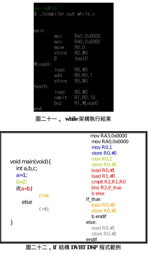
圖二十、while 結構 DVBT DSP 程式範例 在比較指令的部份,DVBT DSP可以作暫存器與暫存器之間的比較,跟暫存 器與立即值之間的比較。將結果值存到暫存器中。分之指令在利用此暫存器的值決定是否要發生跳躍。整個while架構是由WLOOP與test兩個標籤所構成,程 式一開始即跳到test去判斷a是否小於0,如果成才跳到WLOOP中執行while
架構中的指令。WLOOP與test兩個標籤後面的數字功能與FOR迴圈相同。
圖6-7是執行while的結果。 圖二十一、 while 架構執行結果 void main(void){ int a,b,c; a=1; b=2; if(a<b) c=a; else c=b; } mov RA3,0x0000 mov RA0,0x0000 mov R0,1 store R0,#0 mov R0,2 store R0,#1 load R0,#1 load R1,#0 cmplt R2,R1,R0 bnz R2,if_true b else If_true: load R0,#0 store R0,#2 b endif else: load R0,#1 store R0,#2 endif 圖二十二、if 結構 DVBT DSP 程式範例
If的架構方面,是由if_true , else , endif三個標籤所構成,如果if的判斷是 true,則跳到if_true執行,如果是false,則跳到else執行。如果是不完整的if 架構,也就是沒有else 的if,則compiler將不會產生else標籤,在b else的那行 指令會變成b endif。圖6-9跟圖6-10是if架構執行結果。
圖二十三、if else 架構執行結果 圖二十四、if 架構執行結果
void main(viod){ int a; a=0; do{ a++; }while(a<10) } mov RA3,0x0000 mov RA0,0x0000 mov R0,0 store R0,#0 DLoop0: load R0,#0 add R0,R0,1 store R0,#0 load R0,#0 cmplt R1,R0,10 bnz R1,DLoop0 圖二十五、do while 結構 DVBT DSP 程式範例
在do while架構中,跟while的架構差不多,只是判斷放在架構的最後執行, 所以do while架構中的指令至少會被執行一次。圖6-12使是do while架構執行 結果。 圖二十六、do while 架構執行結果 在ARRAY的宣告部份,DVBT DSP compiler的做法跟變數的宣告相同, ARRAY宣告以後,compiler會依序將位移量分配下去。假設宣告的變數為 int a,b,c[4],d,則位移量的分配如下: Offset variable 0 a 1 b 2 c[0] 3 c[1] 4 c[2] 5 c[3] 6 d 表十六、位移分配表
執行結果
void main(){
int a,b,c[4],d;
a=d;
b=c[1];
}
圖二十七、 宣告變數的執行結果由圖x-x可知,在宣告c[4]後,程式執行到a=d,是做load R0,#6跟storeR0,#0, 可見compiler給 d位移量的是6沒錯。
初值的給定
void main(){
int a=1,b,c[]={9,8,7,6};
b=c[0];
}
圖二十八、初值給定的執行結果 由圖6-14可知,當在變數宣告的時候,同時安排初始值的話,在程式的一 開始就會先把值一個一個存到memory中,在開始執行其他指令。執行sort
main(){
int A[]= {11, 2 , 3, 6, 4, 20, 13, 8, 25, 7}; int i, j,tmp;
for(i=0; i< 10; i++){ for( j=0; j<9; j++){ if( A[j]<A[j+1] ){ tmp= A[j]; A[j]=A[j+1]; A[j+1]=tmp; } } } } 圖二十九、一個 bubble sort C 程式
最後對compiler作依個粽合的驗證,我們將一個bubble sort C 程式,送進compiler
結果與討論
第一年的計畫主要在DVBT_DSP微架構的設計與指令集的定義。目前計畫 進行的狀態,已將DVBT_DSP硬體透過模擬軟體與FPGA版驗證完畢,並使用 幾個常在數位訊號處理中使使用的演算法評估效能,以更精確的評估實作上的時 脈限制、成本限制,回饋改進原來的設計,以及克服實作的限制及成效的保證, 從事系統參數調整及結構修正。不過DVBT_DSP應用分析環境正在建立當中, 因此計畫目前執行的進度大約是百分之九十。在下年度的計畫中,主要目標是將 DVBT_DSP處理核心驗證及整合於400MHz之IC晶片,並精確地估計得出各單 元電路大小,即進入第二次電路配置,更詳細地規劃各單元在晶片上的位置及大 小。並依配置上的困難回饋修改原設計。在初步的實作電路整合完成後,在總計 畫的整合驗證環境下,以實際的應用程式、作業系統等,與其他子計畫進行整合 測試,以對設計進行相容性驗證。一但有相容性的問題出現,就要回饋修改原設 計。 DSP核心高階語言支援設計,目前已經可以將C語言轉譯成 DVBT_DSP 的目的 程式。第二年目標實現DSP核心高階語言最佳化編譯器設計,將設計相容於C語言 的高階語言的支援環境,此環境包括高階語言編譯器及除錯環境,並最佳化的轉 譯指令排程以增進DVBT_DSP 的執行效能,以下兩點是預計進行最佳化的方式。 (1) 支援資料流方面有向量化運算與窗型運算(Data Windowing Computing )結構的分析。(2) 支援指令並行方面有零負擔的迴圈(Zero-overhead Looping)、軟式管
道運算(Software Pipelining)與多引線的指令排程( Multi-threading) 的結構分析。
參考文獻
[1] J. F. Parker, et al., “A CMOS continuous-time NTSC-to-color-difference decoder,” IEEE Journal of Solid-State Circuits, Vol. 30, pp. 1524-1532, Dec. 1995.
[2] M. McGinn and J. Alberkrack, “An advanced multi-standard TV video/sound IF,” IEEE Transactions on Consumer Electronics, Vol. 40, pp. 290-298, Aug. 1994.
[3] D.-S. Han, J.-H. Seo, and J.-J. Kim, “Fast carrier frequency offset compensation in OFDM systems,” IEEE Transactions on Consumer Electronics, Vol. 47, pp. 364-369, Aug. 2001.
[4] Y. Wu, E. Pliszka, B. Caron, P. Bouchard, and G. Chouinard, “Comparison of Terrestrial DTV Transmission Systems: The ATSC 8-VSB, the DVB-T COFDM, and the ISDB-T BST-OFDM,” IEEE Trans. Broadcasting, Vol. 46, No. 2, June 2000.
[5] F. Classen and H. Meyr, “Frequency synchronization algorithms for OFDM systems suitable for communication over frequency selective fading channel,” in Proc. IEEE Vehic. Technol. Conf., Stockholm, Sweden, pp. 1655-1659, June 1994.
[6] S. A. Fechtel, “OFDM carrier and sampling frequency synchronization and its performance on stationary and mobile channels,” IEEE Transactions on Consumer Electronics, Vol. 46, pp. 438-441, Aug. 2000.
[7] A. G. Armada, B. Bardon, and M. Calvo, “Parameter optimization and simulated performance of a DVB-T digital television broadcasting system,” IEEE Transactions on Broadcasting, Vol. 44, pp. 131-138, March 1998.
[8] J. Rinne, “Diversity reception schemes for COFDM in a mobile environment utilizing soft-bit information,” IEEE International Conference on Communications 2001, pp. 3041-3045, 2001.
[9] S. Armour, et al., “Complexity evaluation for the implementation of a pre-FFT equalizer in an OFDM receiver,” IEEE Transactions on Consumer Electronics,
Vol. 46, pp. 428-437, Aug. 2000.
[10] S. Cacopardi et al, ”High end implementation of DVB-T OFDM demodulator using general purpose DSPs”, International Conference on Consumer Electronics, pp. 382-383, 1998.
[11] F. Frescura et al, “DSP based OFDM demodulator and equalizer for professional DVB-T receivers”, IEEE Trans. on Broadcasting, vol. 45, No.3, pp. 323-332, September 1999.
[12] C. D. Toso et al, “0.5-um CMOS circuits for demodulation and decoding of an OFDM-based digitl TV signal conforming to the European DVB-T standard”, IEEE Journal of Solid-State Circuits, vol.33, pp. 1781-1791, November 1998. [13] C. C. W. Hui et al, “A 64-point Fourier transform chip for vedio motion
compensation using phase correlation”, IEEE Journal of Solid-State Circuits, vol.31, pp. 1751-1761, November 1996.
[14] E. E. Swartzlander, W. K. W. Young and S.J. Joseph, “A radix-4 delay commutator for fast Fourier transform processor implementation,” IEEE Journal of Solid-State Circuits, vol. SC-19, pp. 702-709, October 1984.
[15] E. E. Swartzlander, V. Jain. And H. Hikawa, “A radix-8 wafer scale FFT processor,” IEEE Journal of VLSI Signal Processing, pp.165-176, May 1992. [16] E. H. Wold and A. M. Despain, “Pipeline and parallel-pipeline FFT processors
for VLSI implementation,” IEEE Transactions on Computers, vol. C-33, pp.414-426, May 1984.
[17] B. Gold and T. Bially, “Parallelism in fast Fourier transform hardware,” IEEE Transactions on Audio Electroacoustics, vol.21, no.1, pp. 5-16,1973.
[18] A. M. Despain, “Fourier transform computer using CORDIC iterations”, IEEE Transactions on Computer, pp. 993-1001, Oct 1974.
[19] A. M. Despain, “Very fast Fourier transform algorithms hardware for implementation,” IEEE Transactions on Computers, vol. C-28, no.5, May 1979. [20] E. Bidet, D. Castelain, C. Joanblanq, and P. Stenn, “A fast single chip
Circuits, vol.30, pp. 300-305, March 1995.
[21] S. He and M. Torkelson, “Design and implementation of a 1024-point pipeline FFT processor”, IEEE Custom Integrated Circuits Conference, pp. 131-134, Santa Clara, CA, May 1998.
[22] B. M. Bass, “A 9.5mW 330usec 1024-point FFT processor”, IEEE Custom Integrated Circuits Conference, pp. 127-130, San Jose, CA, May 1998.
[23] G. Bi and E. Jones, “A pipelined FFT processor for word-sequential data,” IEEE Transactions on Acoustics, Speech, and Signal Processing, vol.37, pp.1982-1985, December 1989.
[24] Yutai Ma, “A effective memory addressing scheme for FFT processors”, IEEE Transactions on Signal Processing, vol.47, No.3 pp. March 1999.
[25] D. Sima, “Superscalar instruction issue”, IEEE Micro, Vol. 17, Sept. 1997, pp. 28-39.
[26] Albert Yu, “The future of microprocessors”, IEEE Micro, Dec 1996, pp. 46-53. [27] Gregory A. Uvieghara, Wen-mei W. Hwu, etc, “An experimental single-chip data
flow CPU”, IEEE J. Solid-State Circuits, Vol. 27, No. 1, Jan. 1992, pp.17-28. [28] Ellen Spertus, and William J. Dally, Experiments with Dataflow on a
General-Purpose Parallel Computer, MIT AI Laboratory Report, April 1994.
[29] P. B. Endecott, “Superscalar instruction issue in an asynchronous microprocessor”, IEE Proc. Comput. Digit. Tech., Vol. 143, No. 5, Sep. 1996, pp. 266-272.
[30] R. S. Nikhil, G. M. Papadopoulos, Arvind, “a multithreaded massively parallel architecture”, ACM, 1992.
[31] Lundberg, M.; Muhammad, K.; Roy, K.; Wilson, S.K., “High-level modeling of switching activity with application to low-power DSP system synthesis”, Proceedings of IEEE International Conference on Acoustics, Speech, and Signal Processing, vol. 4, pp. 1877 - 1880, March 1999.
hardware topology on hardware selection for low power DSP”, Proceedings of International Symposium on Low Power Electronics and Design, pp. 94-96, Aug. 1998.
[33] An-Yeu Wu; Liu, K.J.R.; Zhongying Zhang; Nakajima, K.; Raghupathy, A., “Low-power design methodology for DSP systems using multirate approach”, Proceedings of IEEE International Symposium on Circuits and Systems, ISCAS '96, pp. 292 - 295 vol.4, May 1996.
[34] An-Yeu Wu; Liu, K.J.R.; Zhongying Zhang; Nakajima, K.; Raghupathy, A., “Algorithm-based low-power DSP system design: methodology and verification”, VLSI Signal Processing, VIII, pp. 277 – 286, Sept. 1995.
[35] Prayati, A.; Chun Wong; Marchal, P.; Cossement, N.; Catthoor, F.; Lauwereins, R.; Verkest, D.; De Man, H.; Birbas, A., “Task concurrency management experiment for power-efficient speed-up of embedded MPEG4 IM1 player”, Proceedings of Parallel Processing, pp. 453 – 460, Aug. 2000.
[36] Mun Gi Choi; Yingchun Xu , “A new multimedia network architecture using 3G CDMA2000”, Vehicular Technology Conference, pp. 2937 – 2944, Sept. 2000. [37] Bellas, N.; Hajj, I.; Polychronopoulos, C.; Stamoulis, G., “Energy and
performance improvements in microprocessor design using a loop cache”, Proceedings of International Conference on Computer Design, pp. 378 – 383, Oct. 1999.
[38] Chingren Lee; Jenq Kuen Lee; TingTing Hwang, “Compiler optimization on instruction scheduling for low power”, Proceedings of The 13th International Symposium on System Synthesis, pp.55-60, Sept. 2000.
[39] Talla, D.; John, L.K.; Lapinskii, V.; Evans, B.L., “Evaluating signal processing and multimedia applications on SIMD, VLIW and superscalar architectures”, Proceedings of International Conference on Computer Design, pp. 163 – 172, Sept. 2000.
[40] Sami, M.; Sciuto, D.; Silvano, C.; Zaccaria, V., “Instruction-level power estimation for embedded VLIW cores”, Proceedings of the Eighth International
[41] Frantz, G., “Digital signal processor trends”, IEEE Micro, pp. 52 – 59, vol. 20, Nov/Dec 2000.
[42] Furber, S.B.; Edwards, D.A.; Garside, J.D., “AMULET3: a 100 MIPS asynchronous embedded processor”, Proceedings of International Conference on Computer Design, pp. 329 - 334, Sept. 2000.
[43] Eyre, J.; Bier, J., “The evolution of DSP processors”, IEEE Signal Processing Magazine, pp. 43 – 51, vol.17, March 2000.
[44] Gatherer, A.; Stetzler, T.; McMahan, M.; Auslander, E., “DSP-based architectures for mobile communications: past, present and future”, IEEE Communications Magazine, pp. 84-90, vol. 38, Jan. 2000.
[45] Gunn, J.E.; Barron, K.S.; Ruczczyk, W., “A low-power DSP core-based software radio architecture”, IEEE Journal on Selected Areas in Communications, pp. 574 – 590, vol. 17, April 1999.
[46] Gonzalez, R.; Horowitz, M., “Energy dissipation in general purpose microprocessors”, IEEE Journal of Solid-State Circuits, pp. 1277-1284, vol. 31, Sept. 1996.
[47] Zhao Wu; Wolf, W., “Data-path synthesis of VLIW video signal processors,” 11th International Symposium on System Synthesis, pp 96 -1012-4, Dec 1998. [48] Banerjee, S.; Sheikh, H.R.; John, L.K.; Evans, B.L.; Bovik, A.C., “VLIW DSP vs.
superscalar implementation of a baseline 11.263 video encoder,” Conference Record of the Thirty-Fourth Asilomar Conference on Signals, Systems and Computers, 2000 , pp 1665 -1669 , Vol: 2 , 2000.
[49] Sunghyun Jee; Palaniappan, K., “Dynamically scheduling VLIW instructions with dependency information,” Proceedings. Sixth Annual Workshop on Interaction between Compilers and Computer Architectures, pp 15 -23, 2002. [50] Ebcioglu, K.; Fritts, J.; Kosonocky, S.; Gschwind, M.; Altman, E.; Kailas, K.;
Bright, T., “An eight-issue tree-VLIW processor for dynamic binary translation,” International Conference on Computer Design: VLSI in Computers and Processors, 1998. ICCD '98, pp 488 -495, 5-7 Oct 1998.
[51] Shyh-Kwei Chen; Fuchs, W.K., “Compiler-assisted multiple instruction word retry for VLIW architectures,” IEEE Transactions on Parallel and Distributed Systems, Vol 12, pp 1293 -1304, Dec 2001.
[52] Gray, J.; Naylor, A.; Abnous, A.; Bagherzadeh, N., “VIPER: A 25-MHz, 100-MIPS peak VLIW microprocessor,” Proceedings of the IEEE Custom Integrated Circuits Conference, pp 4.1.1 -4.1.5, 9-12 May 1993.
[53] Wolfe, A.; Fritts, J.; Dutta, S.; Fernandes, E.S.T., “Datapath design for a VLIW video signal processor,” Third International Symposium on High-Performance Computer Architecture, 1997., pp 24 -35, 1-5 Feb 1997.
[54] Talla, D.; John, L.K.; Lapinskii, V.; Evans, B.L., “Evaluating signal processing and multimedia applications on SIMD, VLIW and superscalar architectures,” International Conference on Computer Design, 2000, pp 163 -172.
[55] Moon, S.-M.; Park, S., “Performance analysis of VLIW compilation techniques,” IEE Proceedings- Computers and Digital Techniques, Vol.147 Issue: 2 , pp 117 -123, Mar 2000.
[56] Colwell, R.P.; Hall, W.E.; Joshi, C.S.; Papworth, D.B.; Rodman, P.K.; Tornes, J.E., “Architecture and implementation of a VLIW supercomputer,” Proceedings of Supercomputing '90., pp 910 -919, 12-16 Nov 1990.
[57] Conte, T.M.; Banerjia, S.; Larin, S.Y.; Menezes, K.N.; Sathaye, S.W., “Instruction fetch mechanisms for VLIW architectures with compressed encodings,” Proceedings of the 29th Annual IEEE/ACM International Symposium on Microarchitecture, 1996. MICRO-29. , pp 201 -211, 2-4 Dec 1996.
[58] Agarwala, S.; Koeppen, P.; Anderson, T.; Hill, A.; Ales, M.; Damodaran, R.; Nardini, L.; Wiley, P.; Mullinnix, S.; Leach, J.; Lell, A.; Gill, M.; Golston, J.; Hoyle, D.; Rajagopal, A.; Chachad, A.; Agarwala, M.; Castille, R.; Common, N.; Apostol, J.; Mahm, “A 600 MHz VLIW DSP,” IEEE International Solid-State Circuits Conference, 2002. Digest of Technical Papers. ISSCC. 2002 , Vol. 1 , pp 56 -444, 2002.
retargetable VLIW compiler framework for DSPs with instruction-level parallelism,” IEEE Transactions on Computer-Aided Design of Integrated Circuits and Systems, Vol. 20 Issue: 11 , pp 1319 -1328, Nov 2001.
[60] Sunghyun Jee; Palaniappan, K., “Compiler processor tradeoffs for DISVLIW architecture” International Symposium on Parallel Architectures, Algorithms and Networks, 2002. I-SPAN '02., pp 175 -180, 2002.
[61] Lee, M.; Tirumalai, P.; Ngai, T.-F., “Software pipelining and superblock scheduling: compilation techniques for VLIW machines,” Proceeding of the Twenty-Sixth Hawaii International Conference on System Sciences, 1993, pp 202 -213 , 5-8 Jan 1993.
[62] Seshan, N., “High VelociTI processing [Texas Instruments VLIW DSP architecture],” IEEE Signal Processing Magazine , Vol. 15 Issue: 2 , pp 86 -101, Mar 1998.
[63] Suzuoki, M.; Kutaragi, K.; Hiroi, T.; Magoshi, H.; Okamoto, S.; Oka, M.; Ohba, A.; Yamamoto, Y.; Furuhashi, M.; Tanaka, M.; Yutaka, T.; Okada, T.; Nagamatsu, M.; Urakawa, Y.; Funyu, M.; Kunimatsu, A.; Goto, H.; Hashimoto, K.; Ide, N.; Murakami, H.; Ohtagu, “A microprocessor with a 128-bit CPU, ten floating-point MAC's, four floating-point dividers, and an MPEG-2 decoder,” IEEE Journal of Solid-State Circuits, Vol. 34 Issue: 11 , pp 1608 -1618, Nov 1999.
[64] Stoodley, M.G.; Lee, C.G., “Software pipelining loops with conditional branches,” Proceedings of the 29th Annual IEEE/ACM International Symposium on Microarchitecture, 1996. MICRO-29., pp 262 -273, 2-4 Dec 1996.
[65] Sair, S.; Kaeli, D.R.; Meleis, W., “A study of loop unrolling for VLIW-based DSP processors,” 1998 IEEE Workshop on Signal Processing Systems, SIPS 98. , pp 519 -527, 8-10 Oct 1998.
[66] Lee, L.; Suparjo, B.S.; Wagiran, R.; Sidek, R., “DSP design using VLIW architecture,” IEEE International Conference on Semiconductor Electronics, pp 160 -167, 2000
VLIW DSP,” IEEE International Conference on Acoustics, Speech, and Signal Processing, 2000. ICASSP '00., Vol. 6 , pp 3390 -3393, 2000.
[68] Li Fanghui; Long Teng, “A high-speed real-time digital pulse compression system based on TMS320C6201,” 2001 CIE International Conference on Radar, pp 557 -561, 2001.
[69] Rizzo, D.; Colavin, O., “A video compression case study on a reconfigurable VLIW architecture,” Proceedings of Design, Automation and Test in Europe Conference and Exhibition, pp 540 -546, 2002
[70] Iseli, C.; Sanchez, E., “Spyder: a reconfigurable VLIW processor using FPGAs,” Proceedings. IEEE Workshop on FPGAs for Custom Computing Machines, 1993. , pp 17 -24, 5-7 Apr 1993.
[71] Intel, Intel Itanium 2 Processor Reference Manual, 2002. [72] Lex & yacc / John R. Levine, Tony Mason, Doug Brown
[73] Crafting a Compiler with C Charles N. Fischer and Richard J. Leblanc, Jr.
[74] Compilers : Principles, Techniques and Tools A. V. Aho, R. Sethi and J. D. Ullman
[75] System Software L. L. Beck
計畫相關之著作
[1] Te-Shin Yang, Jih-Ching Chiu,"Improving ILP with the Vectorized Computing Mechanism in VLIW DSP Architectures,"Submit to IEE Proc. Computers & Digital Techniques, Nov. 2003.
[2] Chih-Kang Wu and Jih-Ching Chiu,"Design of Buffering Mechanism for Improving Instruction and Data Stream,"Submit to IEE Proc. Computers & Digital Techniques, Oct. 2003.
[3] Te-Shin Yang and Jih-Ching Chiu,"Vectorized Code Scheduling Method for the FFT Algorithm in VLIW Architecture ,"The Ninth Workshop on Compiler Techniques for High-Performance Computing, pp. 11-14, Mar. 2003.
計畫成果自評
數位訊號處理器核心在數位無線通訊系統晶片設計中,實現演算法設計,扮
演著決定性的角色。當前相關的高效能的DSP 核心的發展如 TI的TMS320C6x
系列、Motorola 的DSP563xx、Lucent Technologics 的DSP16xx、Analog Devices
的 ADSP-2116x與TigerSHARC處理器,提供了各種高效能的技術參考,但若直
接將之應用於 OFDM 的相關技術的開發則將無法提供經濟的因應高資料頻寬的
資料運算需求。基於本實驗室在微處理設計與實作的經驗(曾參與國內P7前瞻性
微處理器設計計劃、曾完成 SiS 公司之 ARM 指令相容之五個 Pipeline Stage 的
CPU 核心設計),提出此計劃,除完成實現符合 OFDM 解調變器演算法運算所
需之高效能數位運算核心之設計外,提供國內在高效能 DSP 晶片設計之前瞻性
學術研究,並能對參與之學生相關能力的訓練培養,以協助國內產業擁有關鍵晶
片的開發技術與人才。本計畫所設計的 DSP 架構是結合VLIW技術與向量式的
管 道 運 算 結 構(Vectorized Pipelining Architecture) 觀 念 的 一 個 可 重 結 構 ( reconfigurable ) 的高度指令並行化的前瞻性的設計,計劃實現 40MHz FPGA SIP 雛型與400MHz之晶片設計與相關程式開發環境,不僅可充分符合於本計劃 的需求,更能應用於高效能的數位訊號處理上,如 Software Radio 的演算處理 需求。 本計劃第一年的目標在於建立 DVBT_DSP 微架構與定義指令集,並建立可以 將 C 語言轉譯成 DVBT_DSP 的目的程式高階指令編譯器雛型,目前已完成 95%的 進度執行率。 已經建立的 DVBT_DSP 架構,主要是由兩個運算核心構成,此運算核心稱為 Super Element (SE)。每個 SE 的執行單元包含兩個部份,分別是 Basic Element 1(BE1)與 Basic Element 2(BE2)。BE1 以一個 16bits 算數邏輯處理器為核心, 另外提供了兩個 Load 單元做 Memory read 與一個 Store 單元做 Memory write 的 位址計算。BE2 則是以一個 16bits 算數邏輯處理器與 16x16bits 的乘法器為核 心,另外提供了一個 Load 單元做 Memory read 與一個 Store 單元做 Memory write 的位址計算。整個 SE 共可提供三個 memory load、兩個 memory write 、2 個 ALU 與一個 Multiplier 的功能,在做一般運算時,BE1 與 BE2 最多可各自獨立