國
立
交
通
大
學
電機學院微電子奈米科技產業研發碩士班
碩
士
論
文
電漿處理氧化鋁鉿閘極介電層之研究
The study of plasma treatment on HfAlO gate dielectrics
研 究 生:蘇明紳 Student:Ming-Shen Su
指導教授:張國明 Advisor:Kow-Ming Chang
電漿處理氧化鋁鉿閘極介電層之研究
The study of plasma treatment on HfAlO gate dielectrics
研 究 生:蘇明紳 Student:Ming-Shen Su
指導教授:張國明 Advisor:Kow-Ming Chang
國 立 交 通 大 學
電機學院微電子奈米科技產業研發碩士班
碩 士 論 文
A ThesisSubmitted to College of Electrical and Computer Engineering National Chiao Tung University
in partial Fulfillment of the Requirements for the Degree of
Master in
Industrial Technology R & D Master Program on Microelectronics and Nano Sciences
January 2008
Hsinchu, Taiwan, Republic of China
電漿處理氧化鋁鉿閘極介電層之研究
研究生:蘇明紳
指 導 教 授 : 張 國 明 博 士
國立交通大學電機學院產業研發碩士班
摘要
隨著場效電晶體的尺寸縮小到1.2奈米以下,以二氧化矽當作閘極介電層, 將產生一些諸如電子穿遂效應的問題。摩爾定律將面臨無法繼續適用的窘境,因 此需以高介電係數材料取代二氧化矽作為閘極絕緣層,其中鉿為基礎的氧化物就 是目前被認為最有可能取代二氧化矽的材料。但是矽和高介電係數材料的介面卻 會有缺陷過多的問題,我們利用電漿氮化來解決此問題。本實驗以鋁-鈦-氧化鋁 鉿-矽之電容結構為分析元件。首先利用金屬有機化學沉積法沉積氧化鋁鉿介電 層。接下來,試片在氧化後立刻去做快速熱退火及各種不同時間的電漿處理,其 氣體來源分別是氮氣,氨氣及一氧化二氮,最後再做快速熱退火去修補電漿處理 後的表面。在不同電漿處理條件下的薄膜電性,經由C-V 和I-V 量測得知。另外 也藉由高溫熱處理、磁滯效應、應力引致漏電流測試、定電壓加壓測試及昇溫量 測來討論各種電漿處理條件下元件的可靠度。在這些條件之中,其中以通三十秒 一氧化二氮電漿的樣品呈現出第二大的電容值(增加了25.1%),最小的漏電流(兩 個數量級的下降),以及優異的可靠度。這是因為一氧化二氮電漿處理中的氮原 子會修補介面的缺陷,而氧原子會增加介面氧化層厚度來抑制漏電流,所以其電 容值及漏電流在被電漿傷害破壞前,會因修補介面的效應而持續的改善。另一方 面,氮氣和氨氣電漿處理在適當製程時間內依然是有效改良電性的方法。The study of plasma treatment on HfAlO gate dielectrics
Student:Ming-Shen Su Advisor:Dr. Kow-Ming Chang
Industrial Technology R & D Master Program of
Electrical and Computer Engineering College
National Chiao Tung University
ABSTRACT
When the MOSFET gate insulator is scaled below 1.2 nm, SiO2 as the gate
insulator will has some serious problems such as direct tunneling. The moore’s law will face difficult condition to continue constantly. Therefore, high dielectric constant material is desired to replace SiO2. The oxide of using Hafnium-based is a most
promising material for future MOSFET gate oxide applications. But the interface of between Si and high dielectric constant material has many defects, we will use plasma nitridation to solve this problem. In this study, we used Al-Ti-HfAlO-Si MIS capacitor as our analysis device. First, we used MOCVD system to deposit HfAlO. After oxidation process, we had an additional post-deposition annealing and then plasma treatment with N2, NH3, or N2O plasma for different process durations. Finally,
the samples are treated by post-nitridation annealing to repair the surface of after plasma treatment. The electrical characteristics of the film under different oxidation conditions were discussed by C-V and I-V curves. Moreover, the reliability of the films under different plasma treatment conditions were discussed by high temperature treatment, hysteresis effect, SILC ( Stress Induced Leakage Current ) profile, CVS ( Constant Voltage Stress ) test and increasing temperature measurement. Among these conditions, the sample treated by N2O plasma for 30 sec represents the second
capacitance ( 25.1 % increasing ), lowest leakage current ( 2 order reduction ), and excellent reliability. Since the nitrogen atoms of N2O plasma treatment can repair the
defects of the interface, the oxygen atoms can form additional interfacial oxide between the high-k/Si interface to suppress the leakage current. The capacitance and the leakage current of the high-k dielectric can be improved by the N2Oplasma treatment before the
plasma damage occurring. On the contrary, the N2 and NH3 plasma treatment of the
誌謝
首先,我要感謝指導教授張國明博士這二年來的指導,老師對做
學問的謹慎態度,以及堅持作研究需要仔細探討物理觀念及機制,給
了我很多啟發,著實讓我獲得了豐碩的研究成果。
其次,實驗室學長陳柏寧學長給予的指導相當受用。在實驗過程
中不斷的給予建議,並提供我寶貴的經驗,使得本論文可以順利的完
成。對於學長這兩年來的照顧,我將永遠感恩於心。
另外,實驗室的同學文全、明聰、鈞凱、永茂、勝軍,大家一起
努力打拚,那種患難與共的感覺相當的美好,我將永遠放在心中不會
忘記。
最後,要感謝我的家人,你們的支持與鼓勵是使我順利取得碩士
學位的原動力。
Contents
Abstract (in Chinese) ...i
Abstract (inEnglish) ...ii
Acknowledgments (in Chinese)... iii
Contents ...iv
Table Captions ...vi
Figure Captions...vi
Chapter 1 Introduction
1.1 Background... 11.2 The problem of poly-silicon gate... 2
1.3 Need for high-k materials... 3
1.4 Carrier Transport in High-k GateDielectrics... 3
1.4.1 Schottky Emission (SE) ... 4
1.4.2 Frenkel-Poole Emission (FP) ... 5
1.4.3 Fowler-Nordheim Tunneling (F-N) ... 6
1.5 Use in industry ... 6
1.6 The choice of High-K materials ... 7
1.7 Why choose HfAlO ... 8
1.8 The Roles of Nitrogen in High-k Gate Dielectric ... 9
1.9 The Effects of Interface Engineering on High-k Gate Dielectric... 10
1.10 Plasma Nitridation ... 10
1.11 Thesis Organization ... 12
2.1 How to deposit HfAlO thin film...13
2.2 MOCVD system...14
2.3 Advantages of MOCVD...15
2.4 Rapid Thermal Annealing system...16
2.5 Plasma treatment system...17
2.6 MIS Capacitors Fabrication Process...17
2.7 The theorem of MIS Capacitors measurement ...19
Chapter 3 Electrical Characteristics of Al/HfO
2/Si MIS Capacitors
3.1 Capacitance-Voltage Characteristics...223.2 Current-Voltage Characteristics ...24
3.3 Summary ... 26
Chapter 4 Reliability of Al/HfO
2/Si MIS Capacitors
4.1 Hysteresis...284.2 Stress Induced Leakage Current (SILC)...29
4.3 Constant Voltage Stress (CVS) ...30
4.4 Thermal reliability………...31
Chapter 5 Conclusions and Future Work
5.1 Conclusions ...325.2 Future Work ...33
Table
………..……….….…34Figure-Chapter 2
...41Figure-Chapter 3
...46Figure-Chapter 4.
...50Reference
………...….57Table Captions
Chapter 1
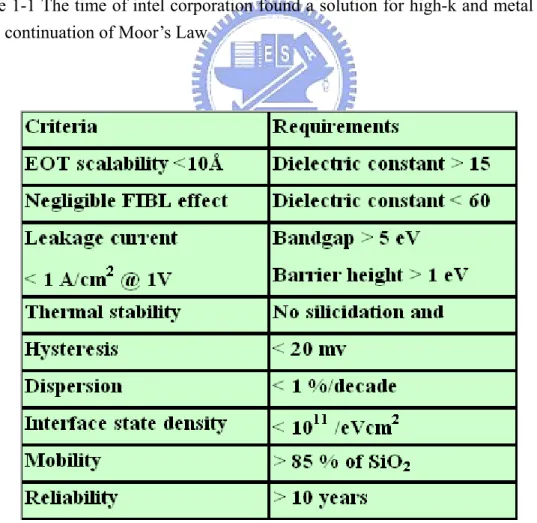
Table 1-1 The time of intel corporation found a solution for high-k and metal gate to keep continuation of Moor’s Law
Table 1-2 Material requirements of high-k dielectrics
Table 1-3 Comparison of relevant properties for various high- k candidates [32].
Chapter 2
Table 2-1 Comparison of deposition techniques: Sputter, ALCVD, and MOCVD [53].
Figure Captions
Chapter 1
Figure 1-1 Illustration of Moore’s law: number of transistors integrated in the different generations of Intel’s microprocessors vs. the production year of these circuits.
Figure 1-2 Trend of device scaling: Transistor physical gate length will reach ~ 15nm before end of this decade and ~ 10nm early next decade.
Figure 1-3 With the marching of technology nodes, gate dielectric has to be shrunk and five silicon atoms thick of gate dielectric is predicted for 2012.[2] Figure 1-4 Measured and simulated Ig-Vgcharacteristics under inversion condition
for nMOSFETs. The dotted line indicates the 1A/cm
2
limit for the leakage current. [3]
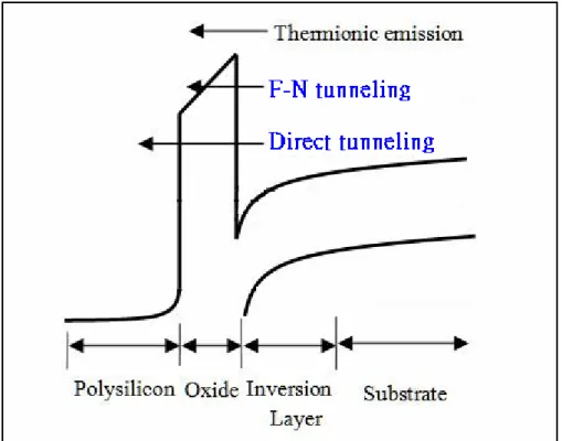
Figure 1-5 Conduction mechanism in oxide for the MOS structure.
Figure 1-6 (a)Energy band chart of NMOS device (b)The influence of poly-Si depletion for capacitance density.
Figure 1-7 High-k+ metal gate transistors provide significant performance increase and leakage current reduction , ensuring continuation of moor’s law. Figure 1-8 Power consumption and gate leakage current density comparing to the
potential reduction in leakage current by an alternative dielectric exhibiting the same equivalent oxide thickness [5].
Figure 1-9 (a)Schottky Emission (SE) (b)Frenkel-Poole Emission (FP)
(c)Fowler-Nordheim Tunneling (F-N) current transport mechanism. Figure 1-10 schemes of important regions in gate stack of a field effect transistor
Chapter 2
Figure 2-1 Schematic diagram of MOCVD system structure.
Figure 2-2 The ICP plasma system that was used in this experiment.
Figure 2-3 (1)Si substrate RCA clean (2)6 nm HfAlO was deposited on the sub-Si by MOCVD.
Figure 2-4 (1) PDA by RTA (2) Plasma treatment (3) PNA by RTA
Figure 2-5 40 nm Ti was deposited on the HfAlO layer by dual e-gun evaporation system .
Figure 2-6 400 nm Al was deposited on the Ti layer as top electrode by thermal evaporation coater.
Figure 2-7 Undefined Al was removed by wet etching
Figure 2-8 Undefined Ti was removed by wet etching (1%HF).
Figure 2-9 Al was deposited on the back side of sub-Si as bottom electrode by thermal evaporation coater.
Figure 2-10 MOS diode capacitance structure
Figure 2-11 The energy band plot and electric charges distribution of MOS diode capacitance under bias voltage.
Figure 2-12 The capacitance-voltage curve of three different conditions
Chapter 3
Figure 3-1 The capacitance-voltage (C-V) characteristics of HfAlO gate dielectrics treated with N2 plasma treatment for different process time.
Figure 3-2 The capacitance-voltage (C-V) characteristics of HfAlO gate dielectrics treated with NH3 plasma treatment for different process time.
Figure 3-3 The capacitance-voltage (C-V) characteristics of HfAlO gate dielectrics treated with N2Oplasma treatment for different process time.
Figure 3-4 The capacitance-voltage (C-V) characteristics of HfAlOgate dielectrics treated with N2 plasma treatment, NH3 plasma treatment and N2O
plasma treatment all for 30 sec.
Figure 3-5 The J-V characteristics of p-type HfAlOcapacitors treated by N2 plasma
with different process time from 0 V to -2 V.
Figure 3-6 The J-V characteristics of p-type HfAlO capacitors treated by NH3
plasma with different process time from 0 V to -2 V.
Figure 3-7 The J-V characteristics of p-type HfAlO capacitors treated by N2O
Figure 3-8 The J-V characteristics of HfAlOgate dielectrics treated with N2 plasma
treatment, NH3 plasma treatment and N2Oplasma treatment all for 30
sec.
Chapter 4
Figure 4-1 The hysteresis of p-type HfAlOgate dielectrics treated without PDA, plasma treatment, PNA.
Figure 4-2 The hysteresis of p-type HfAlOgate dielectrics treated with PDA, N2
plasma treatment, PNA.
Figure 4-3 The hysteresis of p-type HfAlOgate dielectrics treated with PDA, NH3
plasma treatment, PNA.
Figure 4-4 The hysteresis of p-type HfAlOgate dielectrics treated with PDA, N2O
plasma treatment, PNA.
Figure 4-5 The SILC curve of p-type HfAlOgate dielectrics treated with N2 plasma
treatment for different process time.
Figure 4-6 The SILC curve of p-type HfAlO gate dielectrics treated with NH3
plasma treatment for different process time.
Figure 4-7 The SILC curve of p-type HfAlO gate dielectrics treated with N2O
plasma treatment for different process time.
Figure 4-8 The gate current shift of p-type HfAlOgate dielectrics treated with N2
plasma treatment for different process time as a function of stress time during Vg = -3 V CVS stress.
Figure 4-9 The gate current shift of p-type HfAlOgate dielectrics treated with NH3
plasma treatment for different process time as a function of stress time during Vg = -3 V CVS stress.
plasma treatment for different process time as a function of stress time during Vg = -3 V CVS stress.
Figure 4-11 The CVS compare of HfAlOgate dielectrics treated with N2 plasma
treatment , NH3 plasma treatment and N2Oplasma treatment all for 30
sec.
Figure 4-12 The capacitance-voltage (C-V) characteristics of HfAlOgate dielectrics treated with PDA, N2, NH3, N2O plasma treatment all for 30 sec, PNA
plus 950℃ 30 sec.
Figure 4-13 The J-V characteristics of HfAlOgate dielectrics treated with PDA, N2,
NH3, N2O plasma treatment all for 30 sec, PNA plus 950℃ 30 sec.
Figure 4-14 The J-V characteristics of HfAlOgate dielectrics treated with N2 plasma
treatment , NH3 plasma treatment and N2Oplasma treatment all for 30
Chapter 1
Introduction
1.1 Background
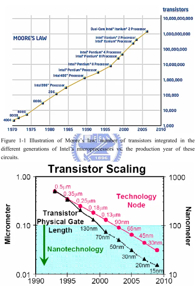
The success of the semiconductor industry relies on the continuous improvement of integrated circuit (IC) performance. This improvement is achieved by reducing the dimensions of metal oxide semiconductor field effect transistor (MOSFET). Size reduction of MOSFET has provided further improvement in speed performance, circuit density, and cost per transistor over the past few decades. As a result, the scaling of MOSFET follows the famous Moore’s law, which predicts the exponential increase in the number of transistors integrated on a chip. Gordon Moore, the Chairman Emeritus of Intel Corporation, made his famous research in 1965 [1]. He observed an exponential growth in the number of transistors per integrated circuit and predicted that this trend would continue. As shown in Fig. 1-1, through Intel's relentless technology advances, "Moore's Law", the doubling of transistors every couple of years has been maintained, and still holds true today. Since the circuit density will continue to increase in the future, further device scaling is needed. As shown in Fig. 1-2, the transistor physical gate length will be expected to down to 15nm in 2010.
Over the past 30 years, SiO
2 has served its role as a perfect gate dielectric, and
node today, in order to gain a large Cg and a higher density. Schulz in Nature
predicted that, in order to keep up with the roadmap goal, in 2012 the thickness of gate oxide is slated to scale down to 1nm, which represents only five silicon atoms thick (see Fig 1-3)[2]. Thus the direct tunneling current which depends strongly on film physical thickness will increase to an unacceptable range, resulting in a huge power dissipation and heat (1.1).
We can see from Fig. 1-4 to find that the gate oxide can be scaled down to 2nm before exceeding the limit of 1A/cm2 from the viewpoint of allowable stand-by power dissipation. As shown in Fig. 1-5, below 2nm the oxide tunneling current will quickly becomes problematic. For easily sensing the seriousness of leakage problem: as SiO
2
thickness is reduced, leakage current increases exponentially (~10×/2Å)[3].
1.2 The problem of poly-silicon gate
For increasing the performance and circuit density of CMOS, scaling down gate length and insulator layer thickness must be done. As the size of CMOS is scaled down, the gate of poly silicon and the insulator layer of SiO2 have problems as
followed:As shown in Fig. 1-6, device with such a small size will aggravates some problems like poly-silicon (poly-Si) gate depletion effect, high gate resistance, dopant penetration from doped poly-Si gate and high gate tunneling leakage current [4]. To alleviate these undesired performances in nanoscale transistors, there is immense interest in the replacement of the conventional materials.
1.3 Need for high-k materials
This rapid shrinking of the transistor feature size has focused the channel length and gate dielectric thickness to also decrease rapidly. This has been reported that the CMOS gate dielectric SiO2 thickness can scale to a least 13 Å [5]. However, while
SiO2 thickness is less than 20-25 Å, large direct-tunneling current is inevitable.
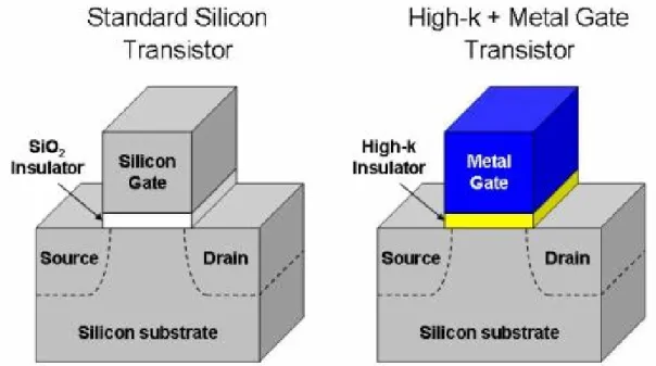
Therefore, as shown in Fig.1-7, it is necessarily for high dielectric constant material (high-κ) gate dielectrics to be studied as alternative gate dielectrics in order to suppress excessive gate leakage current and power consumption.
High-κ gate materials can maintain the same EOT with thicker physical thickness, and is therefore expected drastically reduced direct-tunneling current. From Figure 1-8, the increased physical thickness significantly reduces the probability of tunneling across the insulator, and hence, reduces the amount of off-state leakage current [6].The relationship between dielectrics constant and thickness is followed (1.2):
1.4 Carrier Transport in High-k Gate Dielectrics
The continuous scaling down of gate silicon dioxide thickness in metal oxide semiconductor devices achieve continued improvement in integrated circuit (IC) performance. However, the accompanying high leakage current of thin silicon oxide
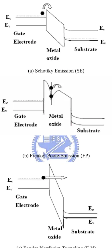
is a significant problem for IC application. A high-k gate dielectric with a large physical thickness, while an identical equivalent oxide thickness has recently been proposed to solve this leakage issue. A survey of the literature on high-k gate dielectric shows that the leakage current densities are strongly dependent on the deposition method, pre-deposition, and post-deposition annealing treatments performed to enhance the properties of high-k gate dielectric [7]. Depending on the applied voltage and the thicknesses of the high-k films, the conduction process identified in Hf-based dielectric is generally attributed to a Schottky emission (SE), the Frenkel-Poole (FP) emission, or Fowler-Nordheim tunneling (F-N). Therefore, it is important to study the various leakage mechanisms in these dielectrics with the aim of minimizing their leakage current for advanced IC devices applications.
1.4.1 Schottky Emission (SE)
The carrier transport mechanism of Schottky emission (SE) in high-k gate dielectric was shown in the Fig 1-10 (a). The SE emission is due to the transport of electrons from gate electrode over the potential barrier into the Si substrate resulting from thermionic emission. The current density (J) – field (E) relation for SE is given by the Schottky-Richardson relation as [8],
(1.3)
whereβSE is given by
(1.4) and
(1.5) withεr is the dynamic dielectric constant, ε0 the permittivity of the free space, k is
the Boltzmann constant and T the absolute temperature; CRD is the Richardson
constant and is expressed as,
(1.6) where m* is the effective mass of electrons in dielectric.
1.4.2 Frenkel-Poole Emission (FP)
The carrier transport mechanism of Frenkel-Poole (FP) emission in high-k gate dielectric was shown in the Fig 1-10 (b). The FP emission is due to the thermal excitation of charge carriers from Coulombic traps in the bulk of a dielectric or semiconductor, enhanced by the application of an electric field. The general expression for the FP current density is given by
(1.7) where Ct is a trap density related constant; qφB is the ionization potential in eV,
which is the amount of energy required for the trapped electron to escape from the influence of the positive nucleus of the trapping center when no field is applied; β
E is the amount by which the trap barrier height is reduced by the applied electric
field, E. The factor ξ in the denominator of the exponential may vary between 1 and 2, depending on the amount of acceptor compensation. Rewriting Eq. (1-5) as
which is referred as the FP plot.
1.4.3 Fowler-Nordheim Tunneling (F-N)
The carrier transport mechanism of Fowler-Nordheim (FN) tunneling in high-k gate dielectric was shown in the Fig 1-10 (c). The FN emission is caused by field ionization of trapped electron into the conduction band or by electrons tunneling from the metal Fermi energy into insulator conduction band. The tunnel emission has the strongest dependence on the applied voltage but is essentially independent of the temperature. The general expression for the F-N current density is given by [9]
(1.9) where C is a function of the electron effective mass
1.5 Use in industry
In early 2007, as shown in table 1-1, Intel announced the deployment of hafnium-based high-k dielectrics in conjunction with a metallic gate for components built on 45 nanometer technologies, expected to ship in 2007. At the same time, IBM announced plans to transition to high-k materials, also hafnium-based, for some products in 2008. While not identified, it is most likely the dielectrics used by these companies are some form of HfSiON. HfO2 and HfSiO are susceptible to crystallization during dopant activation annealing. NEC Electronics has also announced the use of a HfSiON dielectric in their 55 nm Ultimate Low Power technology. However, there is no absolute guarantee that hafnium will be the basis of future high-k dielectrics. The 2006 ITRS roadmap predicts the implementation of high-k materials to be commonplace in the industry by 2010.
1.6 The choice of High-K materials
The replacement of silicon dioxide as a gate insulator in MOS devices by materials of higher dielectric permittivityεr is motivated by the need of increasing
the capacitance density without further reducing the physical thickness. Despite a considerable effort in this direction, the formation of a thin SiO2 interlayer between
silicon substrate and the high-k material appears to be unavoidable [10]. Most of high-k materials are not stable in direct contact with silicon and require a thin SiO2
layer to stabilize the dielectric film on silicon substrate. Thin SiO2 layer can improve
interface states, surface roughness and electron mobility. The use of dielectric layers with high-k will give us thicker films with equivalent SiO2 electrical thickness, and
should allow us to reduce the leakage current and improve the reliability of the gate dielectric layer. Currently many experimental efforts are to investigate for alternative gate dielectric materials. Many metal oxides such as TiO2, Al2O3, Ta2O5, ZrO2 , HfO2,
La2O3, Y2O3, [11-17] etc. and ferroelectric materials (e.g., PZT [18], BST, etc.) are
being investigated as candidate material to replace silicon dioxide. The required material properties of alternative gate oxide can be summarized as follows.
1. Dielectric constant significantly larger than 3.9 in thin film phase. 2. Thermodynamic stability in direct contact with silicon .
3. Low diffusion constant for dopant atoms in poly-Si.
4. Large band gap with more than 1 eV tunneling barrier for both electrons and holes in order to achieve low leakage current.
5. Low interface trap defect density, Dit ≦1010-1011cm-1eV-1. 6. Low defect density within oxide layer.
7. Preferably stable amorphous phase to avoid grain boundary problem.
Table 1-2 illustrates Material requirement of high-k dielectrics. For most high-k materials, the higher dielectric constant comes at the expense of narrow band gap. The lower barrier height for tunneling tend to compensate the benefit of the higher dielectric constant. Even though there are many materials with significantly high k values, many of them are not suitable for gate dielectric applications since they do not satisfy several of these necessary conditions. For example, TiO2 has a higher k value
of 80-100 but has a small band gap of 3.5 eV and band offset of 0.05 eV. Most other ferroelectric materials such as SrTiO3 with very high dielectric constants have the
same problem of small potential barrier [19]. Table 1-3 shows material properties comparison of Al2O3, ZrO2 ,HfO2.
1.7 Why choose HfAlO
HIGH- materials have been studied as alternative gate dielectric materials for high performance and low stand-by power CMOS. Among all high- gate dielectric materials, HfO2 is being extensively investigated as one of the most promising
candidate materials. HfO2 appears promising due to its relatively high dielectric
constant ( 25) as compared to SiN and Al2O3 [20], its relatively high free energy of
reaction with Si (47.6 kcal/mole at 727 C) as compared to TiO2 and Ta2O5 [21] and its
relatively high band gap ( 5.8 eV) among its high-k contenders [22]. It is desirable for high- materials to remain amorphous after device fabrication. However, HfO2
crystallizes at temperatures less than 500℃. Grain boundaries in crystallized gate dielectric can be the fast paths for oxygen or dopants diffusion into gate dielectric and
even FET channel region in silicon substrate, causing uncontrolled interfacial layer growth at the interface, threshold voltage instability, and defect generation. Therefore, there have been several reports on using nitrogen or aluminum incorporation into high- materials to raise the crystallization temperature [20, 21, 23, 24].
1.8 The Roles of Nitrogen in High-k Gate Dielectric
The nitrogen-incorporated gate dielectrics have been shown to possess a higher breakdown field, better crystalline retardation, and reduced leakage current with the same EOT [25]. For electrons injected from the interface, the nitrogen-rich layer near the dielectric/Si substrate interface has the capability of lowering the leakage current tunneling through the dielectric [26].
It has been also reported that the nitrogen in the gate dielectric can reduce the amount of detrimental species diffused from the gate electrode [27]. Moreover, the electrical property degradation of MOS devices is influenced by the concentration of nitrogen in the high-k gate dielectric [28]. In general, either bottom nitrided (BN) or top nitrided (TN) can be used to improve the electrical properties of MOS devices with HfO2, and HfSiO gate dielectric. The 3 BN techniques usingsurface nitridation
has shown reduced leakage current and is effective in preventing boron penetration [29]. The TN approach using a reactive sputtering method to control the nitrogen profile in HfO2 gate dielectric has been reported to possess thermal stability and be
effective in preventing oxygen diffusion through HfO2 [30]. In addition, excellent
electrical properties of MOS devices with HfOxNy gate dielectric have been achieved
by sputtering of HfN layer in an Ar+N2 ambient in comparison with HfO2 [25]. It is
also reported that the nitrogen concentration in HfOxNy gate dielectric can
above indicate that the roles of nitrogen in high-k gate dielectric are important in improving the electrical characteristics of MOS devices.
1.9 The Effects of Interface Engineering on High-k Gate
Dielectric
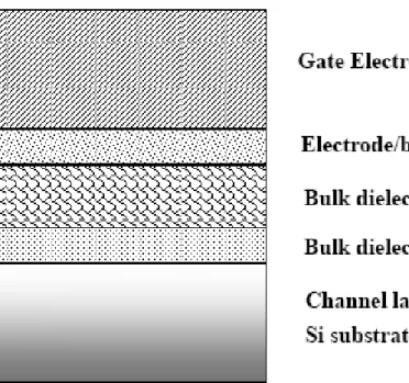
Fig. 1-10 shows the scheme of important regions in gate stack of a field effect transistor [32]. The high-k material/silicon interfaces are regarded as unideal due to the presence of defect states [33]. The originations of these interface defects may be related to the stray metal atoms within the Si adjacent to the interface or due to surface structural defects, oxidation-induced defects, or defects caused by radiation [33-34]. Interface traps have a major impact on device lifetime and play an important role in determining the threshold voltage, inversion layer mobility and low frequency noise of MOS devices, the surface perfection comparable to Si-epitaxial growth required for reduction of interface traps are a significant concern [35-36]. Moreover, interface trap of MOS devices is another major contributor to leakage current besides the characteristics of dielectric material itself. If the interface between dielectric/Si is rough, intensive electric field will take place at the sharp corners which may then lead to a high leakage current and low breakdown voltage [37]. Various processes can influence the interface quality; dry etching is one example [37-38]. Accordingly, to achieve a smooth surface and to form a undamaged layer on substrate is an important task in modern metal-oxide-semiconductor field-effect-transistor (MOSFET) devices [38]. In short, to achieve a good dielectric/Si interface as a surface channel of MOS device, the defect density at silicon surface must be minimized.
According to traditional view of improving SiO2 device performance, we could
find that nitridation is a common method to improve the interface [39]. Property with the result that there is often Nit or Dit in the interface, imperfect bonding of interface
usually makes the characteristic of the device deteriorate. Such as charge will be trapped by the defects of the interface, it produce flat band voltage shift and also reduce mobility. Another shortcoming is that these dangling bonds will easily bond with oxygen atom in the following high temperature environment. The extra chemical reaction will let the interfacial oxide growth, and it will reduce the C value because of the lower dielectric constant. In addition, the quality of interfacial layer formed by oxidation is worse, and it would cause the problem of charge trapping. In order to solve these problems, nitridation treatment could let the atom of nitrogen bond with these dangling bonds and fix it while entering the interface layer, and then improve the stability and reliability of interface. Consequently, nitridation treatment is a workable solution to improve interface quality. As we note before, the question about using high-k materials to replace SiO2 is that there are too many defects in the
interface to cause reliability degradation. Therefore, when we use high-k materials, it is consider that nitridation treatment is a more suitable way to improve reliability and thermal stability of device. These kind of treatment have already used in some relevant references [40] [41]. Among them, someone take nitridation treatment at high temperature, others take so-called plasma nitridation . According to [42], we could understand that the effect of plasma nitridation is better than thermal nitridation. The reason is that high-k materials could not sustain high thermal stress. As long as the temperature reaches certain degree, we would see the phenomenon of crystallization. The crystallization of dielectric would increase leakage current substantially, because it offers the path of leakage current. On the other hand, the meaning of plasma
nitridation is to activate the source gas first. The high activation energy of radical will provide better mend which is better than nitridation at high temperature. For all these reasons, we adopt plasma nitridation in present experience.
1.11 Thesis Organization
Following chapters in the thesis are primarily organized as follow:
In chapter 2, we make a description of experimental details. Metal Organic Deposition system is used to deposit HfAlO material on silicon surface.
In chapter 3, we discuss the characteristics of HfAlO insulator by Metal Insulator Semiconductor (MIS) capacitors.
In chapter 4, we discuss the reliability of HfAlO insulator by Metal Insulator Semiconductor (MIS) capacitors and the effects of Post-Metallization-Annealing.
In chapter 5, we make the conclusions for this thesis and provide some suggestions for future work.
Chapter 2
Experiments of Al/Ti/ HfAlO
/Si MIS Capacitor
2.1 How to deposit HfAlO thin film
There are many methods to deposit high-κ gate dielectrics stack, such as physical vapor deposition (PVD) [43], atomic layer deposition chemical vapor deposition (ALCVD) [44-48], and metal-organic chemical vapor deposition (MOCVD) [49-51]. In the industrial production viewpoint, PVD is not an appropriate tool for high-κ film deposition due to both poor step coverage and bad uniformity. Nowadays, ALCVD and MOCVD have paid more efforts to be evaluated for high-κ dielectrics deposition in the industry. Table 2-1 is the comparison of deposition techniques which have been used. MOCVD has the advantage of superior step coverage, high deposition rate, good controllability of film composition, and excellent thickness uniformity on large dimension wafers. MOCVD system is therefore chosen to deposit high-κ dielectrics in this thesis.
Recently, aluminum oxide (Al2O3) had been proved as promising candidates for
the gate dielectrics of sub-0.1μm device due to their higher κ value, relatively high
φ
Band superior thermal stability [49]. Due to the high dielectric constant and high thermal stability, Al2O3 is suitable to be integrated into trench DRAM process and is
therefore chosen in this thesis. Figure 2-1 shows the detail schematic structure of the MOCVD system. The MOCVD chamber is equipped with a turbo-molecular pump
and a liquid injection system which has four independent-controlled injectors. A liquid pump is consisted of the injector and pumps the precursors through a hot nickel frit with a proper rate. The vapors are carried with a 200 sccm flow of Argon to gas distribution ring which is located at a proper distance from the substrate. On the contrary of the conventional bubbler system, the liquid injection system is with sufficient temperature window to alleviate the thermal aging of the precursor. This is because the precursor remains in liquid state at room temperature until it is pumped into the vaporizer and injected into the deposition chamber. However, the precursor should keep at long-term chemical stability in solvent and non-reactive with other precursors in solvent [52]. The components of the vaporizer, the gas ring and the connecting tube are maintained at 190°C with heating tapes and blankets, while the substrate temperature is controlled at 500 ° C with quartz-halogen lamps and a thermocouple. A rotating susceptor is used for uniformly heating during processing. A flow of 100 sccm N2 is maintained throughout the deposition cycle. The base pressure
of the MOCVD chamber is ~ 10-8torr. The deposition pressure of the deposition is at the 5 mtorr where the gas-phase collisions are scarce.
2.2 MOCVD system
MOCVD (metal-organic CVD) is a widely used technology for depositing a variety of thin films, including metal oxide and metal silicate films, for high-k gate dielectric applications. The basic steps in MOCVD deposition method are as follows: 1. MO precursor in company with N2 process gas and O2 process gas are injected into
the reactor.
2. The sources are mixed inside the reactor and transferred to the deposition process chamber.
of sources and other gas-phase reactions, forming the film precursors that are useful for film growth and byproducts.
4. The film precursors transport to the growth surface. 5. The film precursors absorb on the growth surface. 6. The film precursors diffuse to the growth site.
7. At the surface, film atoms incorporate into the growing film through surface reaction.
8. The byproducts of the surface reactions desorb from the surface.
9. The byproducts transport to the main gas flow region away from the deposition area toward the reaction. Then the wafer exits.
Most of the devices with MOCVD HfO2 and HfSixOy when a poly-Si gate is
used have EOT greater than 2 nm. Unlike metal electrode, using poly-Si electrode requires the high-k gate stack to go through a 1000°C/10 sec S/D activation anneal step. This step not only results in chemical and structural changes in the high-k film, but also affects interfaces between the high-k film/substrate and the high-k/poly-Si electrode. All devices fabricated with MOCVD ZrO2 and ZrSiO films using poly-Si
gate electrode were too leaky to give any meaningful C-V results. In general, using poly-Si gate electrode results in around 0.7 to 1 nm higher EOT for gate stacks fabricated with HfO2 and HfSixOy gate dielectric films. This additional interfacial
oxide thickness is too large to be acceptable. In view of this, the MOCVD is not a good tool for high-k material deposition with poly-Si gate. However, the MOCVD has very good throughput and can process a 25-wafer lot in ~2 hours (roughly 4X better than ALCVD). Thus, from a throughput perspective, the MOCVD has a distinct advantage over the ALCVD [53].
In our study, the depositions of TiO2 thin films were prepared by MOCVD among the most important techniques for depositing thin, high purity epitaxial films with applications in electronics and optics [54]. MOCVD is a very attractive technique which has many advantages, such as: high deposition rate, high crystallization without post annealing, large-area deposition, high throughput, excellent uniformity, excellent step coverage on three-dimensional complex geometries, flexibility for large-scale processing, and a simple experimental system compared to physical vapor deposition which requires high-vacuum equipments. So in this study, low-pressure MOCVD technique was adopted.
2.4 Rapid Thermal Annealing system
METAL RTA-AG 610 was a single-wafer lamp-heated and computer controlled rapid thermal processing (RTP) system. Water and compressed dry air (CDA) cooling system were used to cool down the quartz chamber. High intensity visible radiation heating and cold-heating chamber walls allow fast wafer heating and cooling rate. The tungsten halogen lamps were distinguished into five groups, and the relative percentage of lamp intensity can be adjusted individually for each group to achieve uniform temperature distribution. Temperature was obtained from pyrometer and precise controlled by computer. Two gas lines were used in the system which can be switched between Ar and N2. Before RTA process started, one minute N2 gas
purge was performed to minimize the water vapor introduced during wafer loading and also swept unwanted particles induced during process. A fast heating rate of 100 /s was chosen in this work. When anneal was complete, chamber temperature ℃ was quickly cooled down from 900 to 500 by N℃ ℃ 2 purge 30 seconds. Then, the
chamber was slowly cooled down to 280 without N2 purge to avoid creaking of ℃ films. After five minutes later, wafers can be taken out from the chamber. Films’ creak can be avoided by two-steps-cooling method.
2.5 Plasma treatment system
When the PDA (Post-Deposition-Annealing) was finished, some samples were subjected to an additional plasma treatment in order to improve the electrical properties of gate dielectric. There were various source gas (N2, NH3, N2O) and
process time (10 sec, 30 sec, 60 sec, 90 sec) as the experiment conditions. Parallel plate high-density plasma reactor employing an ICP source was a single-wafer treated and computer-controlled system.
Fig. 2-2 illustrates ICP system that was used in this experiment. 13.56 MHz RF power was coupled to the top electrode through a matching network. After the sample load to reactor, the system was pumped down to keep the chamber clean enough. Subsequently, the source gas was become radical by the plasma system, as the chamber pressure was 100 mTorr and the substrate temperature was 300 ℃ so that to achieve the goal of low temperature process. The power of working plasma was kept constant at 200W and the flow rate of source gas was 100 sccm. While the process of plasma treatment was finished, these samples were brought to thermal treatment to reduce plasma damage.
2.6 MIS Capacitors Fabrication Process
HfAlO gate dielectrics. Figure 2-3 ~ Figure 2-9 shows the fabrication flow of this experiment. The starting wafer was four inch (100) orientated p-type. It was one side polished and its resistivity was 5~10 ohm-cm.
After standard initial RCA cleaning, wafers were put into chamber and grew HfAlO layer with metal organic deposition system. After the thin films were prepared, some samples were annealed after deposition (post-deposition anneal) and then subjected to an additional plasma treatment at the substrate temperature of 300℃ while the pressure was 100 mTorr and the plasma power was 200W. The plasma treatment conditions were in pure N2, NH3 and N2O for 10 sec, 30 sec, 60 sec, and 90 sec
respectively and the flow rate were 100 sccm. After nitridation, we also annealed these samples to reduce the plasma damage. Pure titanic was deposited on the HfAlO layer by dual e-gun evaporation system and aluminum films were thermally evaporated on the top side of wafers. Mask defined the top electrode. Then, we used wet etching to etch undefined Al and Ti films. After patterning, backside native oxide was stripped with diluted HF solution, and Al was deposited as bottom electrode. The detailed fabrication process flow was listed as follows.
1. As shown in Fig.2-3 (1)Si substrate RCA clean
(2)6 nm HfAlO was deposited on the sub-Si by MOCVD.
2. As shown in Fig.2-4
(1) Post-Deposition-Annealing by RTA(800℃-60 sec for HfAlO) .
(2) Plasma treatment with N2 , N2O or NH3 (10 sec,30 sec, 60 sec, 90 sec) .
3. As shown in Fig.2-5
40 nm Ti was deposited on the HfAlO layer by dual e-gun evaporation system .
4. As shown in Fig.2-6
400 nm Al was deposited on the Ti layer as top electrode by thermal evaporation coater.
5. As shown in Fig.2-7
Undefined Al was removed by wet etching (H20:CH3COOH : H3PO4:HNO3) .
6. As shown in Fig.2-8
Undefined Ti was removed by wet etching (1%HF).
7. As shown in Fig.2-9
Al was deposited on the back side of sub-Si as bottom electrode by thermal evaporation coater.
After the Al/Ti/HfAlO /Si MIS capacitors were prepared, we used semiconductor parameter analyzer (HP4156C) and C-V measurement (HP4284) to analysis electric characteristics (i.e. I-V, C-V, EOT, leakage current density etc.). Then we tested their reliability, including stress induced leakage current (SILC), constant voltage stress (CVS), hysteresis effect.
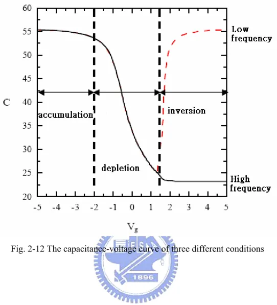
As shown in Fig.2-10, the theorem of we use on capacitance measurement is: we add a constant DC bias on the metal gate and then add a small AC signal of different frequency. Due to AC signal is changing constantly so the electric charges of being attracted are changing constantly, too. As the result of the above-mentioned, we will get the capacitance using the changing amount of the electric charges divided by the changing amount of the voltage (2.1).
We will illustrate the three different conditions of ideal MOS diode capacitance under three different bias voltage. As shown in Fig. 2-11, the first condition, we add a minus bias voltage on the metal gate and then the energy band of the interface between oxide layer and semiconductor bend upward. The interface will attract some holes to accumulate around and we name this condition: accumulation. This is real oxide capacitance.
The second condition, we add a small positive bias voltage and then the energy band bend downward. The holes of around interface will be repel and form a depletion layer. We name this condition: depletion. Due to the measurement capacitance is the oxide capacitance series connect depletion capacitance so the capacitance is smaller. The third condition, we add a large positive bias voltage on the metal gate and then the energy band bend downward drastically. The interface around will not only form depletion layer but also attract some electrons. When the numbers of minority electrons are more than majority holes and the surface will form inversion phenomenon. We name this condition is: inversion. If the measurement frequency is high frequency, the capacitance is constant due to the width of depletion layer up to maximum. If the measurement frequency is low frequency, the recombination and generation rate of the minority carrier will catch up with the changing of low
frequency. The carrier changing will happen at interface around totally and the capacitance is larger and larger up to oxide capacitance [55, 56]. The capacitance-voltage curves of three conditions are shown in Fig. 2-12.
Chapter 3
Electrical Characteristics of Al/Ti/HfAlO/Si MIS
Capacitors
3.1 Capacitance-Voltage Characteristics
In order to measure the C-V characteristics of our MIS capacitors we used HP2484C LCR meter in our experiments. We swept the gate bias from inversion region to accumulation region to obtain the curve at the frequency of 50 kHz. There are three kinds of plasma treatment with different source gas ( i.e. N2, N2O, and NH3 )
and they were treated for different process time ( i.e. 10 sec, 30sec, 60 sec,90 sec). Firstly, the relationship of difference process time in one kinds of plasma treatment will be discussed. Then compare with the effect of different source gas.
Fig. 3-1 reveals the capacitance-voltage (C-V) characteristics of HfAlOgate dielectrics treated with N2 plasma treatment for different process time. The capacitor
treated for 10 sec and 30 sec shows almost the same maximum capacitance among these conditions of process time. In addition, the capacitor treated for 60 second show the good C values which are larger then the capacitor with the condition of origin. This phenomenon indicates that the N2 plasma treatment was workable to
improve the capacitance. Maybe it is caused of the intensifying of the interface structure or high-k bulk itself. The growing of interfacial oxide has also been restrained. On the other hand, the capacitance treated for 90 sec is very low and it is even lower than the no-treated sample. It is seems that the plasma damage occur and then destroy the structure of high-k capacitance when the duration of plasma
treatment is too long. The degradation of capacitance also can be found at the case of 60 sec treatment time, although the C value is still larger then the case without plasma treatment.
Fig. 3-2 shows the capacitance-voltage (C-V) characteristics of HfAlO gate dielectrics treated with NH3 plasma treatment for different process time. Just like the
group of N2 plasma treatment. The improvement of capacitance and the damage cause
by excessive plasma treatment both can be seen. At this condition, the capacitance treated with NH3 plasma treatment for 30 second shows the largest value. Then, the
capacitance becomes worse and worse with the increase of the treatment time. By the way, the samples besides 60 sec and 90 sec all have larger capacitance than the original sample. It is indicated that NH3 plasma treatment is also a practicable method
to improve the capacitance-voltage characteristics of HfAlOgate dielectrics.
Fig. 3-3 shows the capacitance-voltage (C-V) characteristics of HfAlO gate dielectrics treated with N2O plasma treatment for different process time. The
experiment of plasma treatment only with oxygen radical is wanted to see if it is still existed the improvement of capacitance. Consequently, it is shown that the capacitors treated for 10 sec, 30 sec, 60 sec and 90 sec have larger capacitances than the origin sample, especially for 30ses provided the maximum capacitance. Take the view of 90 sec condition, its capacitance curve shift larger than the other samples. Besides 90 sec conditions, the other samples still remain good capacitances than origin sample. So it can be know that the long plasma time will damage the sample. It is suggested that plasma treatment with oxygen radical may cause additional oxidation followed by repairing of the interface structure. Because the interfacial oxide provides lower k value, the total capacitance was be affected and become lower.
Fig. 3-4 shows the capacitance-voltage (C-V) characteristics of HfAlO gate dielectrics treated with N2, NH3 andN2Oplasma treatment all for 30 sec. It is indicated
that the capacitance treated with N2 plasma treatment for 30 sec shows the most
excellent value (i.e. 31.1% increasing about capacitance). Among these samples, the capacitance treated with NH3 plasma treatment is the worst because NH3 has the least
N atoms to repair defects and dangling bonds. NH3 has hydrogen atoms to bond with
dangling bonds but the bond is weak. The capacitance treated with N2O plasma
treatment is the second because N2O has oxygen atoms and the growing of interfacial
oxide is unavoidable while the oxygen atoms become radical and enter the interface. This is the reason why the sample treated with N2O plasma has lower capacitance
than N2 plasma treatment. It is may be the growing of interfacial oxide made the
capacitance degradation. Thus, the capacitance improvement by interface repair was easily eliminated by the interfacial oxide which has lower k value.
3.2 Current-Voltage Characteristic
Fig. 3-5 shows the J-V characteristics of p-type HfAlOcapacitors treated by N2
plasma with different process time from 0 V to -2 V. We observed that the gate leakage current density is suppressed while treatment conditions are 10sec, 30sec, 60 sec. It is indicated that N2 plasma treatment supply an effective barrier against the
leakage current. The lower leakage shows that the weak structure of interface must be fixed by the plasma nitridation, especially for 30 sec capacitor which both has the lowest leakage and largest capacitance value from Fig. 3.1. Gate leakage current density of origin insulator at VG = -1 V is about 2.5×10⁻⁴ A/cm2. From fig.3-5,
however, gate leakage current density of the capacitor treated for 30 sec N2 plasma at
about 2 orders. Furthermore, we notices that the 60 sec capacitor although has little leakage, its capacitance has become degradation. This is an interesting phenomenon. Even though the plasma damage has begun to reduce C value, the amount of leakage current is still kept very well. It means that the capacitance value is more easily affected by plasma damage than leakage current. By the way, the 90 sec sample has the larger leakage current value than original that because the too long plasma time will damage the sample.
Fig. 3-6 shows the J-V characteristics of p-type HfAlO capacitors treated by NH3 plasma with different process time from 0 V to -2 V. After NH3 plasma treatment,
we can see the reduction of leakage current in contrast of original sample. It is worthy to be noticed that the capacitors treated by 30 sec NH3 plasma which has the best C
value also performs a low leakage current about 7.98×10⁻⁶A/cm2. In addition, we find that the leakage current of 10 sec treatment are larger than the other sample, but they are all not larger than original sample. Relative to the case of N2 plasma, we can see
that the level of leakage current increasing obviously mitigate.
Fig. 3-7 shows the J-V characteristics of p-type HfAlOcapacitors treated by N2Oplasma with different process time from 0 V to -2 V. Besides 60 sec sample, the
other samples depict the presence of the reduction in leakage current. It is indicated that there are not only the effect of improving interface quality but also another effect to suppress the leakage current in the case. According to the discussion about Fig. 3-3, we know that the growth of interfacial oxide layer will decrease the C value. Now the interfacial layer introduces a hard barrier to suppress leakage current. Consequently, the leakage current all displays a lower value including the capacitor treated by N2O
Fig. 3-8 shows the J-V characteristics of HfAlOgate dielectrics treated with treated with N2, NH3 andN2Oplasma treatment all for 30 sec. We find that N2Oplasma
treatment all for 30 sec has the lowest leakage current compared with N2, NH3 both for
30 sec. It is possibly due to the additional oxidation layer formed by oxygen atom. The interfacial oxidation layer will let the dielectric thicker to prevent from gate leakage. It is proved that without thick oxidation layer, it can also reach the smallest leakage current when there is suitable time treatment.
3.3 Summary
By the compare of the samples which has the best capacitance in their own gas, we can realize the most suitable treatment condition which both has the best capacitance and lowest leakage current. But from Fig. 3-4 and Fig. 3-8 show that no any plasma gas has the both advantages, we must find a relative optimum condition. It is showed that the N2 plasma treatment for 30 sec has the maximum C value and the
third leakage current compared with N2 and NH3 both for 30 sec. On the other hand, it
is showed that the NH3 plasma treatment for 30 sec has the second C value and the
second leakage current compared with N2 and N2O both for 30 sec. Finally, N2O
plasma treatment for 30 sec has the second C value and the lowest leakage current compared with N2 and NH3 both for 30 sec. We can determine the N2O sample to be
the relative optimum condition among our all samples.
If we take a look at all the samples, we find that the N2, N2O, and O2 plasma
treatment all shows better electrical properties than original sample. Furthermore, the N element can fix the interface and promote the electrical properties include of CV curve and JV curve. But for the reason of oxidation caused by oxygen radical, the
N2O plasma treatment samples shows the lower C value than N2. Just because the
oxidation phenomenon, the films will become thicker so that the plasma damage will not easily affect the leakage current profile.
Chapter 4
Reliability of Al/HfAlO/Si MIS Capacitors
4.1 Hysteresis
The name of Hysteresis was borrowed from electromagnetics. It is means that when a ferromagnetic material is magnetized in one direction, it will not relax back to zero magnetization when the applied magnetizing field is removed. It must be driven back to zero by the additional opposite direction magnetic field. If an alternating magnetic field is applied to the material, its magnetization will trace out a loop called a hysteresis loop [34].
The hysteresis phenomenon is similar in the C-V curve of the MIS capacitor device. When we apply a voltage in opposite direction, it will not fit the original C-V curve measured previously. It is due to the traps of interface which can trap charges to influence the flat band voltage and C-V curve. [23] Fig. 4-1 shows the hysteresis of p-type HfAlOgate dielectrics treated without PDA, plasma treatment and PNA and the hysteresis is 83 mV. Fig. 4-2 shows the hysteresis of p-type HfAlOgate dielectrics treated with N2 plasma treatment for 30 sec process time. Hysteresis of p-type HfAlO
capacitors is changed with the plasma treatment and it’s value is 6 mV. The hysteresis is suppressed by means of the fixing ability at the interface .
Fig. 4-3 shows the hysteresis of p-type HfAlOgate dielectrics treated with NH3
the case of N2 plasma treatment and it’s value is 7 mV. Fig. 4-4 shows the hysteresis
of p-type HfAlOgate dielectrics treated with N2Oplasma treatment for 30 sec process
time and it’s value is 8 mV. It also shows a likely tendency. As a consequence, the plasma treatment can improve the reliability of hysteresis all for the different plasma gas treatment. Among these samples, we can find that the hysteresis of N2 plasma
treatment for 30 sec is the smallest but three hysteresis values are almost the same. Therefore, we can speculate that the sample without plasma treatment which is not very good at quality of interface oxide layer so that the charge was be trapped at the interface and introduce hysteresis.
4.2 Stress Induced Leakage Current (SILC)
In order to investigate the reliability of MIS capacitor device, the stress induced leakage current is a common experiment. The machine about SILC is the stress induced trap density in the bulk in thin film. The trap density introduce new leakage path. Fig. 4-5 shows the SILC curve of p-type HfAlOgate dielectrics treated with N2
plasma treatment for 30 sec process time. After the stress of -3 constant voltage for 180 second, the gate leakage current become larger than before. The degree of leakage current degradation can be judged for the reliability of MIS capacitor. From Fig. 4-5, it displays the improvement of SILC compared with the capacitor of the original sample. Almost all the samples are considered that have smaller increasing of leakage current after SILC than original sample. On the other hand, it is also can be noticed that the SILC of 90 sec treated sample become worse due to the plasma damage.
Fig. 4-6 and Fig. 4-7 display the SILC curve of p-type HfAlOgate dielectrics treated with NH3 plasma treatment and N2Oplasma treatment respectively. They all
show the distinct improvement as long as they are treated with plasma treatment. So the plasma treatment including of N2, NH3, and N2Oas source gas can have the
reliability of devices to suppress SLIC.
4.3 Constant Voltage Stress (CVS)
To study the reliability of HfAlOfilm, stressing the film with a constant voltage or a constant current are two common methods. The machine about CVS is the charge trapping by the interfacial trap density which is caused by stress for long time. Furthermore, the mount of charges cause more interface trap density and from new leakage path to add leakage. In our experiments, we use constant voltage stress (CVS) to test the reliability of HfAlOfilm. Fig. 4-8 shows gate current shift of p-type HfAlO gate dielectrics treated with N2 plasma treatment for different process time as a
function of stress time during Vg = -3 V CVS stress. From the condition of 10 sec to 30 sec, the current shift is smaller and smaller. Then the current shift begins to become great by the damage of plasma at the process time of 60 sec and 90 sec . Fig. 4-9 shows gate current shift of p-type HfAlOgate dielectrics treated with NH3 plasma
treatment for different process time as a function of stress time during Vg = -3 V CVS stress. It has similar behavior about the trend compared with N2. Fig. 4-10 shows gate
current shift of p-type HfAlOgate dielectrics treated with N2Oplasma treatment for
different process time as a function of stress time during Vg = -3 V CVS stress. While the 30-sec treated sample presents the lowest current shift, the 90 sec treated sample become to be destroyed by the plasma damage. Fig. 4-11 shows the CVS compare of HfAlOgate dielectrics treated with N2 plasma treatment , NH3 plasma treatment and
N2Oplasma treatment all for 30 sec. We find the leakage current shift of three plasma
treatment almost the same.
4.4 Thermal reliability
Fig. 4-12 shows the capacitance-voltage (C-V) characteristics of HfAlOgate dielectrics treated with PDA, N2, NH3, N2O plasma treatment all for 30 sec, PNA plus
950℃ 30 sec. We find that after 950℃ 30 sec the capacitance of all the samples are decreasing smaller than 10%. Fig. 4-13 shows the J-V characteristics of HfAlOgate dielectrics treated with PDA, N2, NH3, N2O plasma treatment all for 30 sec, PNA plus
950℃ 30 sec. We find that after 950℃ 30 sec the capacitance of all the samples are increasing about one order. Fig. 4-14 The J-V characteristics of HfAlOgate dielectrics treated with N2 plasma treatment , NH3 plasma treatment and N2Oplasma treatment
all for 30 sec and then measured at 25℃ and 125℃. We find that the leakage current is increasing slightly.
Chapter 5
Conclusions and Future work
5.1 Conclusions
In this thesis, we used the post-deposition annealing, plasma treatment and post-nitridation to enrich the HfAlOfilm quality. The plasma treatment conditions are N2, NH3, and N2Oplasma for 10 sec, 30 sec, 60 sec, 90 sec individually. Several
important phenomena were observed and summarized as follows. First of all, improvement in the electrical characteristics of Al/Ti/HfAlO/Si MIS capacitors using plasma treatment has been demonstrated in this work. All of the plasma treatment can promote the electrical characteristics and reliability until the plasma damage happened. Among these treatments, the sample using N2, NH3 and N2Oplasma all for 30 sec
represent fairly great improvement, such as good capacitance (31.1 %, 19.0 % and 25.1 % increasing respectively at -2 V ), reduced leakage current (about 2 order reduction ). It is showed that the formation of interfacial layer has been suppressed and the weak structure of interface has been repaired by N2, NH3 and N2Oplasma
respectively. Besides, the sample treated by N2, NH3, and N2Oplasma all for 30 sec
also show excellence promotion about reliability issue, such as smaller hysteresis ( 6 mV, 7 mV, 8 mV respectively), less SILC and better CVS curve. These advancements were ascribed to the good interface quality. On the other hand, the N2O plasma
treatment has the lowest leakage current. The reason is that the samples using N2O
that the capacitance will be lower than N2. But for another hand, the thicker oxidation
layer becomes a good resistance against leakage current. Finally, in this thesis, the point we focus on both the improvement of capacitance and leakage current. The treatment of N2Oplasma for 30 sec is the relative optimum condition because it has
the second capacitance improvement (25.1 % increasing) and the first leakage current improvement (about 2 orders reduction). Simultaneously, its reliability also represents a excellent progress.
5.2 Future work
1. The goal of low leakage current:
We must try to research the other new process and the other gas plasma treatment to reduce the defects and suppress the leakage current in HfAlO thin film further.
2. More potential interfacial layer investigation:
The quality of the interfacial layer still must be improved. Moreover, in order to improve the quality at high-k/Si-substrate interafce, other more potential interfacial layers maybe can be investigated in the future. For example:HfSiON.
3. Devices fabrication with the above results:
The optimum condition will be used to the structures of our MOS device in the future.
Table
Table 1-1 The time of intel corporation found a solution for high-k and metal gate to keep continuation of Moor’s Law
Table 1-3 Comparison of relevant properties for various high- k candidates [32].
aCalculated by Robertson. bMono.=monoclinic. cTetrag.=tetragonal.
Figure-chapter 1
Figure 1-1 Illustration of Moore’s law: number of transistors integrated in the different generations of Intel’s microprocessors vs. the production year of these circuits.
Figure 1-2 Trend of device scaling: Transistor physical gate length will reach ~ 15nm before end of this decade and ~ 10nm early next decade.
Fig. 1-3 With the marching of technology nodes, gate dielectric has to be shrunk and five silicon atoms thick of gate dielectric is predicted for 2012.[2]
Fig. 1-4 Measured and simulated Ig-Vgcharacteristics under inversion condition for nMOSFETs. The dotted line indicates the 1A/cm2 limit for the leakage current. [3]
Fig. 1-5 Conduction mechanism in oxide for the MOS structure.
Figure 1-6 (a) Energy band chart of NMOS device (b) The influence of poly-Si depletion for capacitance density.
Fig. 1-7 High-k+ metal gate transistors provide significant performance increase and leakage current reduction , ensuring continuation of moor’s law.
Figure 1-8 Power consumption and gate leakage current density comparing to the potential reduction in leakage current by an alternative dielectric exhibiting the same equivalent oxide thickness [5].
(a) Schottky Emission (SE)
(b) Frenkel-Poole Emission (FP)
(c) Fowler-Nordheim Tunneling (F-N)
Figure 1-9 (a) Schottky Emission (SE) (b) Frenkel-Poole Emission (FP) (c)Fowler-Nordheim Tunneling (F-N) current transport mechanism.
Figure 1-10 schemes of important regions in gate stack of a field effect transistor
Figure-chapter 2
Fig. 2-2 The ICP plasma system that was used in this experiment.
Fig.2-3 (1)Si substrate RCA clean (2)6 nm HfAlO was deposited on the sub-Si by MOCVD.
Fig.2-4 (1) PDA by RTA (2) Plasma treatment (3) PNA by RTA
Fig.2-5 40 nm Ti was deposited on the HfAlO layer by dual e-gun evaporation system .
Fig.2-6 400 nm Al was deposited on the Ti layer as top electrode by thermal evaporation coater.
Fig.2-7 Undefined Al was removed by wet etching .
Fig.2-8 Undefined Ti was removed by wet etching (1%HF).
Fig.2-9 Al was deposited on the back side of sub-Si as bottom electrode by thermal evaporation coater.
Fig. 2-10 MOS diode capacitance structure
Fig. 2-11 The energy band plot and electric charges distribution of MOS diode capacitance under bias voltage.
Figure-chapter 3
-2.0 -1.5 -1.0 -0.5 0.0 0.5 1.0 0.0 2.0x10⁻⁷ 4.0x10⁻⁷ 6.0x10⁻⁷ 8.0x10⁻⁷ 1.0x10⁻⁶ 1.2x10⁻⁶ origin8000C-60sec+N2-10sec+6000C-60sec
8000C-60sec+N2-30sec+6000C-60sec
8000C-60sec+N2-60sec+6000C-60sec
8000C-60sec+N 2-90sec+600 0 C-60sec
Capacitance (F/cm
2)
Voltage(V)
Fig.3-1 The capacitance-voltage (C-V) characteristics of HfAlO gate dielectrics treated with N2 plasma treatment for different process time.
-2.0 -1.5 -1.0 -0.5 0.0 0.5 1.0 0.0 2.0x10⁻⁷ 4.0x10⁻⁷ 6.0x10⁻⁷ 8.0x10⁻⁷ 1.0x10⁻⁶ 1.2x10⁻⁶ origin 8000C-60sec+NH 3-10sec+600 0 C-60sec 8000C-60sec+NH3-30sec+6000C-60sec 8000C-60sec+NH3-60sec+6000C-60sec 8000C-60sec+NH3-90sec+6000C-60sec
Capacitance (F/
c
m
2
)
Voltage(V)
Fig.3-2 The capacitance-voltage (C-V) characteristics of HfAlO gate dielectrics treated with NH3 plasma treatment for different process time.
-2.0 -1.5 -1.0 -0.5 0.0 0.5 1.0 0.0 2.0x10⁻⁷ 4.0x10⁻⁷ 6.0x10⁻⁷ 8.0x10⁻⁷ 1.0x10⁻⁶ 1.2x10⁻⁶ origin 8000C-60sec+N2O-10sec+600 0 C-60sec 8000
C-60sec+N2O-30sec+6000C-60sec
8000C-60sec+N2O-60sec+600
0 C-60sec
8000C-60sec+N2O-90sec+6000C-60sec
Capacitance (F/cm
2
)
Voltage(V)
Fig.3-3 The capacitance-voltage (C-V) characteristics of HfAlO gate dielectrics treated with N2Oplasma treatment for different process time.
-2.0 -1.5 -1.0 -0.5 0.0 0.5 1.0 0.0 2.0x10⁻⁷ 4.0x10⁻⁷ 6.0x10⁻⁷ 8.0x10⁻⁷ 1.0x10⁻⁶ 1.2x10⁻⁶ origin 8000C-60sec
8000C-60sec+N2-30sec+6000C-60sec 8000C-60sec+NH3-60sec+6000C-60sec
8000C-60sec+N2O-90sec+6000C-60sec
Cap
acitan
ce (F
/cm
2)
Voltage(V)
Fig.3-4 The capacitance-voltage (C-V) characteristics of HfAlO gate dielectrics treated with N2 plasma treatment, NH3 plasma treatment and N2O plasma treatment all
-2.0 -1.5 -1.0 -0.5 0.0 10-8 10-7 10-6 10-5 10-4 10-3 10-2 10-1 origin
8000C-60sec+N2-10sec+6000C-60sec
8000C-60sec+N2-30sec+6000C-60sec
8000C-60sec+N
2-60sec+600
0 C-60sec
8000C-60sec+N2-90sec+6000C-60sec
G
ate Leakage ( A/
cm
2
)
Voltage(V)
Fig. 3-5 The J-V characteristics of p-type HfAlOcapacitors treated by N2 plasma with
different process time from 0 V to -2 V.
-2.0 -1.5 -1.0 -0.5 0.0 10-8 10-7 10-6 10-5 10-4 10-3 10-2 10-1 origin
8000C-60sec+NH3-10sec+6000C-60sec
8000C-60sec+NH
3-30sec+600
0 C-60sec
8000C-60sec+NH3-60sec+6000C-60sec
8000C-60sec+NH 3-90sec+600 0 C-60sec
G
a
te Leakage ( A/cm
2)
Voltage(V)
Fig. 3-6 The J-V characteristics of p-type HfAlOcapacitors treated by NH3 plasma
![Table 1-3 Comparison of relevant properties for various high- k candidates [32].](https://thumb-ap.123doks.com/thumbv2/9libinfo/8754770.206629/47.892.221.670.115.341/table-comparison-relevant-properties-various-high-k-candidates.webp)
![Fig. 1-3 With the marching of technology nodes, gate dielectric has to be shrunk and five silicon atoms thick of gate dielectric is predicted for 2012.[2]](https://thumb-ap.123doks.com/thumbv2/9libinfo/8754770.206629/49.892.170.727.123.492/marching-technology-nodes-dielectric-shrunk-silicon-dielectric-predicted.webp)