Sol-gel-derived double-layered nanocrystal memory
Fu-Hsiang Ko, Hsin-Chiang You, and Tan-Fu Lei
Citation: Applied Physics Letters 89, 252111 (2006); doi: 10.1063/1.2416248
View online: http://dx.doi.org/10.1063/1.2416248
View Table of Contents: http://scitation.aip.org/content/aip/journal/apl/89/25?ver=pdfcov Published by the AIP Publishing
Articles you may be interested in
A TiAl 2 O 5 nanocrystal charge trap memory device Appl. Phys. Lett. 97, 143504 (2010); 10.1063/1.3496437
Device characteristics of HfON charge-trap layer nonvolatile memory J. Vac. Sci. Technol. B 28, 1005 (2010); 10.1116/1.3481140
A high- k Tb 2 TiO 5 nanocrystal memory
Appl. Phys. Lett. 96, 102904 (2010); 10.1063/1.3354027
Novel coexisted sol-gel derived poly-Si-oxide-nitride-oxide-silicon type memory J. Vac. Sci. Technol. B 25, 2568 (2007); 10.1116/1.2794327
Droplet evaporation-induced ferritin self-assembled monolayer as a template for nanocrystal flash memory Appl. Phys. Lett. 90, 193512 (2007); 10.1063/1.2737362
This article is copyrighted as indicated in the article. Reuse of AIP content is subject to the terms at: http://scitation.aip.org/termsconditions. Downloaded to IP: 140.113.38.11 On: Thu, 01 May 2014 01:40:47
Sol-gel-derived double-layered nanocrystal memory
Fu-Hsiang Koa兲
Institute of Nanotechnology, National Chiao Tung University, Hsinchu 300, Taiwan
Hsin-Chiang You and Tan-Fu Lei
Institute of Electronics Engineering, National Chiao Tung University, Hsinchu 300, Taiwan
共Received 26 September 2006; accepted 13 November 2006; published online 20 December 2006兲 The authors have used the sol-gel spin-coating method to fabricate a coexisting hafnium silicate and zirconium silicate double-layered nanocrystal 共NC兲 memories. From transmission electron microscopic and x-ray photoelectron spectroscopic analyses, the authors determined that the hafnium silicate and zirconium silicate NCs formed after annealing at 900 ° C for 1 min. When using channel hot electron injection for charging and band-to-band tunneling-induced hot hole injection for discharging, the NC memories exhibited superior Vth shifting because of the higher
probability for trapping the charge carrier. © 2006 American Institute of Physics. 关DOI:10.1063/1.2416248兴
Conventional flash memory devices possess a floating gate structure in which the charge carrier is stored in a poly-silicon film.1Because the storage charge leaks readily when the tunneling oxide layer is thinner than 85 nm, floating gate structures face severe scaling issues resulting from defects in the tunneling oxide.2 A discrete single-layered nanocrystal 共NC兲 memory was proposed recently as a replacement of the single poly-Si film of a floating gate structure.3–7NC memo-ries can preserve the trapped charge efficiently—i.e., they avoid the problems associated with the charge loss of con-ventional flash memories—while also displaying desirable features such as fast program/erase speeds, low programing potentials, and high endurance.8,9
Many methods have been developed recently for the preparation of a range of NC memories using physical vapor deposition,4,5 chemical vapor deposition 共CVD兲,6 and ion beam synthesis.7 Wang et al.4 formed Ge NCs through the cosputtering of Ge, Al2O3, and HfO2. Yeh et al.5deposited a
nickel layer through electron beam evaporation; prior to forming NiSi2 NCs through annealing at 900 ° C, an
amor-phous Si film was deposited. Liu et al.6self-assembled SiGe NCs from a mixture of GeH4 and Si2H6 gases in a room-temperature CVD system. Muller et al.7implanted Si+ ions into an SiO2layer to form Si NCs.
In addition to these versatile deposition methods for forming NCs, an alternative single-layer NC preparation technique—using a sol-gel spin-coating method—was pub-lished recently.10During NC formation through spin coating, the sol-gel system of interest was blended in the solution. The most valuable feature of using this sol-gel method is that the precursors and equipment are relatively cheap. We be-came interested in investigating whether double-layered NCs would perform better than single-layered NCs memories.
In this study, we used a sol-gel spin-coating method to fabricate a double-layered NC memory. HfCl4 共99.5%,
Ald-rich兲, ZrCl4 共99.5%, Aldrich兲, and SiCl4 共99.5%, Aldrich兲 precursors were dissolved in isopropanol共IPA兲 共Fluka; water content:⬍0.1%兲 to prepare a mother solution in which the HfCl4: ZrCl4: SiCl4 molar ratio was 1:1:1. We combined
HfCl4, ZrCl4, and SiCl4to fabricate coexisting hafnium
sili-cate共HfSixOy兲 and zirconium silicate 共ZrSimOn兲 NC memo-ries.
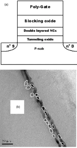
Figure1共a兲illustrates the fabrication of the sol-gel spin-coating NC memories, beginning with a local oxidation of silicon isolation process on a p-type 共100兲 150 mm silicon
a兲Electronic mail: [email protected] FIG. 1.image of hafnium silicate and zirconium silicate NCs.共a兲 Device structure of the double-layered NC memory. 共b兲 TEM
APPLIED PHYSICS LETTERS 89, 252111共2006兲
0003-6951/2006/89共25兲/252111/3/$23.00 89, 252111-1 © 2006 American Institute of Physics
This article is copyrighted as indicated in the article. Reuse of AIP content is subject to the terms at: http://scitation.aip.org/termsconditions. Downloaded to IP: 140.113.38.11 On: Thu, 01 May 2014 01:40:47
substrate. A 4-nm-thick tunneling oxide was grown thermally in a furnace at 925 ° C. The charge trapping layer was depos-ited through spin coating at 3000 rpm for 60 s at ambient temperature 共25 °C兲 using a TEL Clean Track Model-MK8 apparatus 共Japan兲. After spin coating, the wafer was sub-jected to rapid thermal annealing at 900 ° C for 60 s in an O2
ambient to form the coexisting HfSixOy and ZrSimOn NC memory. A 30-nm-thick blocking oxide was deposited through low-pressure chemical vapor deposition tetraethy-lorthosilicate 共LPCVD TEOS兲, followed by deposition of a 200-nm-thick poly-Si gate. After the LPCVD TEOS deposi-tion, the TEOS oxide was densified in a N2 ambient by
an-nealing at 900 ° C for 30 s. Finally, gate pattering, source/
drain implanting, and the remaining steps of the
complementary metal-oxide semiconductor processes were performed to fabricate the double-layered NC memory.
The high-resolution transmission electron microscopy image in Fig.1共b兲clearly depicts the transformation of sol-gel film into NCs after annealing at 900 ° C for 60 s; we observe two differently colored NCs in this image. We used x-ray photoelectron spectroscopy 共XPS兲 to characterize the nature of the chemical bonding in the NCs. Figure2provides a comparison of the XPS results for共a兲 Hf 4f and 共b兲 Zr 3d bonding in the as-deposited 共as-dep兲 and 900 °C-annealed samples. The Hf 4f peaks for the hafnia film 共as-dep兲 ap-peared at 17.4 and 19 eV, while the Zr 3d peaks for the zirconia film共as-dep兲 appeared at 181.9 and 184.3 eV. Inter-estingly, these peaks for both Hf 4f and Zr 3d shifted toward higher bonding energies after annealing to form the NCs.
This observation suggests that the oxygen atoms of Hf–O and Zr–O bonds reacted with their nearby Si atoms, forming hafnium silicate and zirconium silicate.11,12The darker NCs in Fig.1共b兲are those of high-molecular-weight hafnium sili-cate; the bright NCs are formed from low-molecular-weight zirconium silicate.
NC memories use channel hot electron injection共CHEI兲 for charging and band-to-band tunneling-induced hot hole injection 共BTBHHI兲 for discharging. The charge and
dis-charge speeds are closely related to the trapping
probability13,14 of the NCs. Briefly, the electron carrier in Fig.3共a兲can be trapped in the HfSixOyNCs共e.g., see Ref.
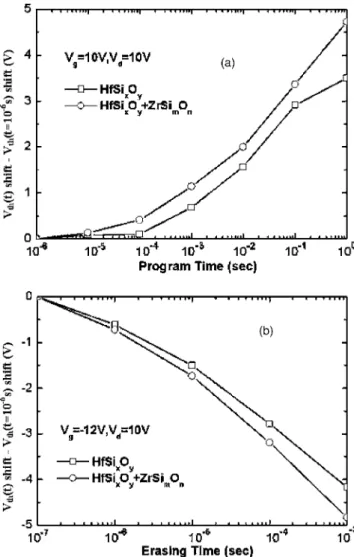
FIG. 4.共a兲 Program and 共b兲 erase speeds of the single- and double-layered NC memories.
FIG. 2. 共a兲 Hf 4f and 共b兲 Zr 3d XPS spectra of as-deposited and 900 ° C-annealed samples.
FIG. 3. Trapping model for the共a兲 single- and 共b兲 double-layered NC memories.
252111-2 Ko, You, and Lei Appl. Phys. Lett. 89, 252111共2006兲
This article is copyrighted as indicated in the article. Reuse of AIP content is subject to the terms at: http://scitation.aip.org/termsconditions. Downloaded to IP: 140.113.38.11 On: Thu, 01 May 2014 01:40:47
10兲 during the charging period. As the hole carrier is injected into the NCs, the trapping capability can influence the dis-charging speed. In other words, the double-layered NCs in this study may offer a higher trapping probability for the charge carrier than do the single-layered NCs. Figure 3共b兲 illustrates the trapping model through which the double-layered NCs improve the hole/electron trapping probability.
Figure4共a兲displays the charging speeds of both a single-layered memory10 and the double-layered NC memory. We used CHEI to program共charge兲 the system under conditions of Vgand Vdboth being 10 V. Obviously, the double-layered NC memory exhibited a larger value of “Vth共t兲 shift–Vth共t
= 10−6s兲 shift” than did the single-layered NC memory. For
example, the values of Vth共t兲 shift–Vth共t=10−6s兲 shift at
1 ms were 0.68 and 1.14 V for the single- and double-layered NC memories, respectively; i.e., the value of Vth共t兲 shift–Vth共t=10−6 s兲 shift was improved by 68%, presumably
because of the better charge carrier trapping probability of the latter system. We are unaware of any other report de-scribing the performance for double-layered NC memories. Figure4共b兲 displays the discharging speeds of the single-10 and double-layered NC memories. We used BTBHHI to erase 共discharge兲 the system under conditions where is Vg and Vdwere −12 and +10 V, respectively. Again, the double-layered NC memory exhibited a significant value of Vth共t兲
shift–Vth共t=10−6 s兲 shift relative to that of the single-layered
NC memory; we also attribute this phenomenon to the higher trapping probability of the double-layered NCs.
In summary, we have used a sol-gel spin-coating method to fabricate a double-layered NC memory. From transmission electron microscopy共TEM兲 and XPS analyses, we confirmed that the NCs consisted of hafnium silicate and zirconium
silicate. The double-layered NCs in this study provided a higher trapping probability for charge carriers than did the corresponding single-layered NC devices.
This study was supported financially by the National Science Council, Taiwan, through Contract No. NSC 95-2113-M-009-032-MY3 and NSC 95-2120-M-009-003.
1Z. Liu, C. Lee, V. Narayanan, G. Pei, and E. C. Kan, IEEE Trans. Electron Devices 49, 1606共2002兲.
2B. D. Salvo, C. Gerardi, R. V. Schaijk, S. A. Lombardo, D. Corso, C. Plantamura, T. Serafino, G. Ammendola, M. V. Duuren, P. Goarin, W. Y. Mei, K. V. D. Jeugd, H. Baron, M. Gély, P. Mur, and S. Deleonibus, IEEE Trans. Device Mater. Reliab. 4, 377共2004兲.
3Y.-N. Tan, W.-K. Chim, B. J. Cho, and W.-K. Choi, IEEE Trans. Electron Devices 51, 1143共2004兲.
4Y. Q. Wang, J. H. Chen, W. J. Yoo, Y.-C. Yeo, S. J. Kim, R. Gupta, Z. Y. L. Tan, D.-L. Kwong, A. Y. Du, and N. Balasubramanian, Appl. Phys. Lett. 84, 5407共2004兲.
5P. H. Yeh, C. H. Yu, L. J. Chen, H. H. Wu, P. T. Liu, and T. C. Chang, Appl. Phys. Lett. 87, 193504共2005兲.
6Y. Liu, S. Tang, and S. K. Banerjee, Appl. Phys. Lett. 88, 213504共2006兲. 7T. Muller, K.-H. Heinig, W. Moller, G. Bonafos, H. Coffin, N. Cherkashin, G. B. Assayag, S. Schamm, M. Tence, and C. Colliex, Appl. Phys. Lett.
85, 2373共2004兲.
8M. She and T.-J. King, IEEE Trans. Electron Devices 50, 1934共2003兲. 9M. Takata, S. Kondoh, T. Sakaguchi, H. Choi, J.-C. Shim, H. Kurino, and
M. Koyanagi, Tech. Dig. - Int. Electron Devices Meet. 2003, 553. 10H.-C. You, T.-H. Hsu, F.-H. Ko, J.-W. Huang, and T.-F. Lei, IEEE Electron
Device Lett. 27, 644共2006兲.
11G. D. Wilk, R. M. Wallace, and J. M. Anthony, J. Appl. Phys. 87, 484 共2000兲.
12P. D. Kirsch, C. S. Kang, J. Lozano, J. C. Lee, and J. G. Ekerdt, J. Appl. Phys. 91, 4353共2002兲.
13W.-T. Lu, P.-C. Lin, T.-Y. Huang, C.-H. Chien, M.-J. Yang, I.-J. Huang, and P. Lehnen, Appl. Phys. Lett. 85, 3525共2004兲.
14M. Ishii and B. Hamilton, Appl. Phys. Lett. 85, 1610共2004兲.
252111-3 Ko, You, and Lei Appl. Phys. Lett. 89, 252111共2006兲
This article is copyrighted as indicated in the article. Reuse of AIP content is subject to the terms at: http://scitation.aip.org/termsconditions. Downloaded to IP: 140.113.38.11 On: Thu, 01 May 2014 01:40:47