國 立 交 通 大 學
電機與控制工程研究所
碩 士 論 文
一個低硬體成本消耗,適用於晶片內單通道每秒
三十億筆資料傳輸之匯流排介面電路設計
A low hardware overhead bus circuit design for
3Gbps/ch on-chip data communication
研 究 生:馬英豪
指導教授:蘇朝琴 教授
億筆資料傳輸之匯流排介面電路設計
A low hardware overhead bus circuit design for 3Gbps/ch
on-chip data communication
研 究 生:馬英豪 Student : Ying Hao Ma
指導教授:蘇朝琴 教授 Advisor : Chau Chin Su
國 立 交 通 大 學
電機與控制工程研究所
碩士論文
A Thesis
Submitted to Department of Electrical and Control Engineering College of Electrical Engineering and Computer Science
National Chiao Tung University in partial Fulfillment of the Requirements
for the Degree of Master
in
Electrical and Control Engineering September 2007
Hsinchu, Taiwan, Republic of China
三十億筆資料傳輸之匯流排介面電路設計
研究生 : 馬英豪 指導教授 : 蘇朝琴 教授
國立交通大學電機與控制工程研究所
摘 要
本論文提出一個使用嵌入式中繼器來降低全區域連接線功率及面積消耗的最佳化理 論。為了平衡全區域連接線的頻寬、功率及面積的消耗,利用一個公制的比較表來使得全 區域連接線設計可以到達最高的效能。我們可以獲得擁有最高公制比較值的全區域連接線 且利用 HSPICE 比較過後的模組。其模擬結果顯示,在電壓為 1.8 伏特時,對於傳統的最 佳化設計,此公制比較值至少增加了百分之七十五。 在本篇論文中,我們實現了一個在晶片內部傳輸線頻寬為每秒三十億筆資料,傳輸距 離為一公分的電路。使用台積電 0.18μ m 1P6M CMOS 製程來實現,此全區域傳輸線電路 在 1.8 伏特的電源供應下消耗功率9.2 毫瓦。 關鍵字: 最佳化,連接線,全區域連接線,中繼器,嵌入式緩衝器,最佳化連接線寬度及 行距,最佳化頻寬3Gbps/ch on-chip data communication
Student: YingHao Ma Advisor: ChauChin Su
Department of Electrical and Control Engineering
National Chiao Tung University
Abstract
This thesis proposes an optimal method to reduce the power consumption and area of global interconnects by buffer insertion. In order to balance the bandwidth, the power, and the area, the figure of merit is introduced to guide the design of the global interconnects to achieve high performance. The optimal design is obtained and result is compared with HSPICE simulation. The simulation results show that at 1.8V the figure of merit increases 75% as compared to other conventional design.
To verify the design, a 3Gbps for 10mm long on-chip interconnects has been designed. It is implemented in TSMC 0.18μ m 1P6M CMOS process, the global interconnects consume 9.2mW on a 1.8V power supply.
Keyword: Optimization, interconnect, global interconnects, repeater, buffer insertion, optimal interconnect width and spacing, optimal bandwidth.
碩士班的兩年研究生涯一轉眼即將結束,回首過去這兩年在交大生活的點點滴滴,辛 苦卻充滿樂趣。當初做研究一切的挫折和磨練,都是讓自己成長的契機,能有這些成果, 要感謝許多在我身旁的人、事、物,因為你們,我的研究生活才能如此多彩多姿。 論文得以順利完成,首先要感謝我的指導教授 蘇朝琴 老師,感謝老師指導我的研究 以及做研究的精神,老師對於研究的嚴謹態度,深深值得我去學習。此外,老師教導我的, 除了專業領域的知識及技術,還有待人處事應有的態度,讓我了解到「遇到困難時,必須 以勇敢、積極的態度去面對它並克服它,千萬不能有逃避的想法,且不可以有後悔的想法, 要堅持此信念,做事才會成功。」老師這兩年來的啟蒙與指導,點點滴滴感謝在心頭。 感謝我親愛的父親及母親,沒有你們無怨無悔的付出,就不會有今天的我,感謝你們 多年的不求回報地辛苦養育,接下來就換我來孝順你們了。感謝你們一直支持我,做我的 後盾,讓我可以專心完成我的學業。最後,你們的態度及智慧就像是人生的寶藏,給了我 許多引導和啟發,使我終身受用。 感謝家楹(妮妮),從認識到現在也快六年了,這期間經歷了不少喜怒哀樂,但也是互 相體諒扶持走了過來。謝謝你陪我渡過了這兩年的碩士生涯,當我在心情低落的時候,妳 除了聽我的抱怨,也給予我最溫暖的支持與鼓勵,讓我有堅持下去的動力。 當然也要感謝學長們兩年來的照顧。謝謝丸子,費心的建置實驗室裡的工作站及電腦 設備,讓我在一個優良的環境下設計晶片,也謝謝你對於我們生活上的照顧;謝謝仁乾, 在我有疑問的時後都會熱心指導我;謝謝盈杰,謝謝你陪我打球,當我的心靈老師,舒緩 了研究上的壓力,還要感謝煜輝、楙軒、宗諭、智琦、小冠、匡良、順閔等諸位學長的細 心指導。 感謝我的同學及學弟們:小潘潘、議賢,有你們兩個在,生活就不會無聊,我會懷念 一起打嘴砲的歡樂時光的,忠傑、教主、方董,918 慢跑隊的成員,在一起跑步的優閒時 光就好像在昨天一樣,祥哥、Snoopy、村鑫、存遠、皇如、雅婷、子俞、碩廷、孔哥、阿 伯、挺毅、季慧,每位都在生活和課業上給了我許多的照顧及幫助,大家的友誼豐富了我 在918 的生活,留下令人難忘的美好回憶。當然,還有助理雅雯、俊秀、上容,感謝妳們 對於我們的照顧及幫忙。 馬英豪 2007.9.30
List of Contents
List of Contents ...V
List of Tables...VII
List of Figures... VIII
Chapter 1 ...1
Introduction...1
1.1INTRODUCTION………..1 1.2MOTIVATION………..2 1.3THESIS ORGANIZATION……….4Chapter 2 ...5
Background Study...5
2.1ELMORE DELAY………5 2.2EFFECTIVE RESISTANCE………6 2.3CROSSTLAK EFFECT………..82.4OPTIMZATION FOR MINIMUM DELAY………9
2.5OPTIMZATION FOR POWER DISSIPATION………..10
2.6 SUMMARY………...12
Chapter 3 ...13
Global Interconnects Circuit Design...13
3.1GLOBAL INTERCONNECTS………...13
3.2MODEL PARAMETER………14
3.3MODEL OF GLOBAL INTERCONNECTS………..15
3.4PERFORMANCE OF GLOBAL INTERCONNECTS………..16
3.6OPTIMZATION FLOW………29
3.7OPTIMAL DESIGN PARAMETER………30
3.8 SUMMARY………...31
Chapter 4 ...32
Global Interconnects Circuit Implementation ...32
4.1SINGLE INTERCONNECT STRUCTURE………...32
4.2GLOBAL INTERCONNECTS STRUCTURE………34
4.3 GENERATION OF RANDOM DATA………36
4.4OUTPUT BUFFER……….38
4.5 LAYOUT AND SIMULATION………39
4.6 PERFORMANCE COMPARISON………44 4.7 MEASUREMENT CONSIDERATIONS………46 4.8 SUMMARY………47
Chapter 5 ...48
Conclusion ...48
5.1 CONCLUSION………48 5.2 FUTURE WORK………49Bibliogrphy..………50
List of Tables
Table 3.1 Technology and equivalent circuit parameters…………....………14
Table 3.2 Optimal design expression………...30
Table 3.3 Optimal design value………30
Table 4.1 Power and jitter of the single interconnects……….33
Table 4.2 Jitter of the global interconnects for 5000μm………..40
Table 4.3 Power and jitter of the global interconnects for 10000μm………...41
Table 4.4 Summary of the 10mm global interconnects………44
Table 4.5 Specifications of the global interconnects………45
List of Figures
Figure 1.1: Basic system-on-a-chip………2
Figure 1.2: High hardware overhead, Medium design complexity………3
Figure 1.3: Low hardware overhead, High design complexity………..3
Figure 1.4: Low hardware overhead, Low design complexity………...3
Figure 2.1: RC ladder for Elmore delay………5
Figure 2.2: (a) Lumped RC model (b) distributed RC model………6
Figure 2.3: Lumped and distributed RC circuit response………...7
Figure 2.4: Crosstalk effects………...8
Figure 2.5: Normalized delay per unit length……….9
Figure 2.6: Basic repeater model………..10
Figure 2.7: Normalized power per unit length……….11
Figure 3.1: Repeater RC model………15
Figure 3.2: Cross section of global interconnects………16
Figure 3.3: Extracted capacitance Cw……….………..16
Figure 3.4: Global interconnects with repeater insertion……….17
Figure 3.5: Switching power model of repeater………...18
Figure 3.6: Voltage and current waveforms of a CMOS inverter……….19
Figure 3.7: Area of a single interconnect with repeater insertion………21
Figure 3.8: MATLAB simulation for power vs. width and spacing………21
Figure 3.9: MATLAB simulation for bandwidth vs. width and spacing……….22
Figure 3.10: MATLAB simulation for area vs. width and spacing……….22
Figure 3.11: MATLAB simulation for product of power and area………..25
Figure 3.12: Variation of bandwidth with number of repeaters….………..26
Figure 3.13: Variation of bandwidth per energy with number of repeaters…………..27
Figure 3.14: Variation of bandwidth per energy with number of repeaters…………..28
Figure 3.15: Optimization flow for global interconnects……….29
Figure 4.1: Single interconnect with the optimal design………..32
Figure 4.2: Corners of the single interconnect……….33
Figure 4.3: Unidirectional global interconnects………...34
Figure 4.4: Geometrical RC model of the parallel interconnect………..34
Figure 4.5: Layout of on-chip global interconnects……….35
Figure 4.6: Impact of interleaving repeaters……….35
Figure 4.7: Resettable dynamic DFF………36
Figure 4.9: Timing diagram of PRBS………...37
Figure 4.10: Eye diagram of PRBS………..37
Figure 4.11: Architecture of output buffer………38
Figure 4.12: Layout of 10mm optimal global interconnects………39
Figure 4.13: Corners of the global interconnects for 5000μm……….40
Figure 4.14: Corners of the global interconnects for 10000μm………...41
Figure 4.15: The eye diagram of global interconnects at 2.2Gbps………...42
Figure 4.16: Temperature = 0 for the global interconnects….………..………...43
Figure 4.17: Temperature = 100 for the global interconnects...………...43
Chapter 1
Introduction
1.1 Introduction
High-density very large scale integration (VLSI) systems use deep submicron (DSM) technology in recent years. With technology scaling, more and more functional blocks are integrated on a chip. The number of transistors per chip is expected to reach one billion by current technologies. The bandwidth and the length of the long global interconnects also increase.
A simplified system-on-a-chip (SOC) is show in Figure 1.1. When the circuits continue to be scaled rapidly past the 180-nm technology node, the chip performance of these ICs are dominated by the global interconnects. The affected performances are as follows. First, the gate delay and the local interconnect delay decrease rapidly with technology advancement. But the global interconnect delay increases for the long interconnect. Therefore, the global interconnect delay is critical. It is an important
metric to optimize the global interconnects. Second, the number of bits per second is another performance for the global interconnects. It is as important as the global interconnect delay for high-performance systems.
SOC TX1,2,3 RX1,2,3 SOC TX1,2,3 RX1,2,3
Figure 1.1 Basic system-on-a-chip
1.2 Motivation
In SOC, the function of the global interconnects is used to link a large number of modules. The length of interconnects are not exactly the same. In Figure 1.2, the same transmitters and receivers transmit the data for the different interconnect length. It has high hardware overhead and medium design complexity. Furthermore, in Figure 1.3, the adaptable transmitters and receivers are used to transmit the data for the different length. It has low hardware overhead and high design complexity. Besides the design complexity, to composite the previous two methods, we observe that these methods have the defect of high power consumption and overall chip area.
On chip channel On chip channel
Figure 1.2 High hardware overhead, Medium design complexity
On chip channel On chip channel
Figure 1.3 Low hardware overhead, High design complexity
We compose the previous two methods. In Figure 1.4, we use the repeater insertion to transmit the data for the different interconnect length. The features of the repeater insertion include: simple circuit design, low power consumption, small area overhead, applicable to multi-channel communication. The signal is transmitted on full swing style on on-chip interconnect. Such that, the global interconnects can be optimized by repeater insertion.
On chip channel On chip channel
1.3 Thesis organization
This thesis comprises five chapters summarized as below:
Chapter 1 reviews the performances of high-speed link impacted by the various technology. The different methods are discussed to transmit data on the global interconnects. Then we present the motivation to optimize the global interconnects by repeater insertion.
In Chapter 2, we introduce the different optimization methods for global interconnects. The different optimizations include two methods. One is to optimize the delay. Another is to optimize the power. Besides, we also discuss their performances aspects.
In Chapter 3, we develop a novel optimization to improve the performance for overall chip. This chapter describes the fundamental methodology, design considerations, and optimal design flows. It shows how to decide the width, spacing, length, bandwidth, and repeater size.
Chapter 4 shows the global interconnects circuit design and implementation. It contains the implementation of the global interconnects circuit which include 10mm interconnect and pseudo random binary sequence (PRBS) generator. The post layout-simulation results, overall chip layout, specification, comparison, and measurement consideration are also shown in this chapter.
Chapter 2
Background Study
2.1 Elmore Delay
The ON transistors are considered as resistors. A chain of transistors is represented as a RC ladder. It is shown in Figure 2.1. The Elmore delay model [1] estimates the delay of an RC ladder as the sum over each node in the ladder of the resistance Rn i− between that node and a supply multiplied by the capacitance on the node : 1 N i pd n i i i j i i j i t R C− C R = = =
∑
=∑ ∑
. (2.1) C1 R1 Vin(t) C2 R2 C3 R3…
CN RN C1 R1 Vin(t) C2 R2 C3 R3…
CN RN2.2 Effective Resistance
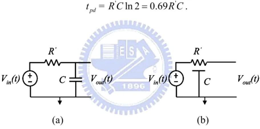
According to the Elmore delay model, a gate with effective resistance R and capacitance has a propagation delay of RC. A wire with distributed resistance R and capacitance C treated as a single π-segment has propagation delay of RC/ 2. We review the properties of RC circuits. The lumped RC circuit in Figure 2.2(a) has a unit step response of
'
-t R C out
V (t)= 1- e . (2.2)
The propagation delay of this circuit is obtained by solving for t when pd
( )
out pd V t = 0.5 : ' ln 2 0.69 ' pd t = R C = R C. (2.3) C Vout(t) R’ Vin(t) C Vout(t) R’ Vin(t) C Vout(t) R’ Vin(t) C R’ Vout(t) Vin(t) C R’ Vout(t) Vin(t) C R’ Vout(t) Vin(t) (a) (b)Figure 2.2 (a) Lumped RC model (b) distributed RC model
The distributed RC circuit in Figure 2.2(b) has no closed form time domain response. The capacitance is distributed along the circuit rather than all being at the end. We expect the capacitance to be charged on average through about half the resistance and the propagation delay is about half as great. It is shown in Figure 2.3. A numerical analysis finds that the propagation delay is0.38R C . '
0 0.5 1 Distributed Lumped tpd 0.5 1 1.5 2 2.5 3 ' -t R C out
V (t)
0 0.5 1 Distributed Lumped tpd 0.5 1 1.5 2 2.5 3 ' -t R C outV (t)
Figure 2.3 Lumped and distributed RC circuit response
To reconcile the Elmore model with the true results for a logic gate, we recall that logic gates have complex nonlinear I-V characteristics and are approximated to have an effective resistance. If we characterize that effective resistance as R R= 'ln 2, the propagation delay really becomes the product of the effective resistance and capacitance: tpd =RC. We will calculate this effective resistance by simulating the delay of a gate driving a capacitance load and measuring the propagation delay.
For the distributed circuits, we observe that
' 1 ' 1
0.38 ln 2
2 2
R C≈ R C = RC. (2.4) Therefore, the Elmore delay model describes distributed delay well if we use an effective wire resistance equal to 69% of that computed with (2.5).
l R R
w
= , . (2.5) This is somewhat inconvenient. The effective resistance is further complicated by the effect of nonzero rise time on propagation delay. When the input is a slow ramp, the propagation delay depends on the rise time of the input and approaches RC for lumped models and RC/ 2 for distributed models.
In summary, it is a reasonable practice to estimate propagation delay of gates using the Elmore delay model as RC where R is the effective resistance of the gate. Similarly, we can estimate the flight time along a wire as RC/ 2 where R is the true resistance of the wire. It is important to use good transistor models and appropriate input slopes to obtain more accurate results.
2.3 Crosstalk Effect
In deep sub-micron technology, the signal over long interconnect is a dominant issue in the chip design with the current technology. With the device sizes getting smaller and smaller and many circuits are built in a chip, the global interconnects are spaced closer and closer together. The signal rise and fall times go into the nano second region, and the effect of coupling is more observable between interconnects.
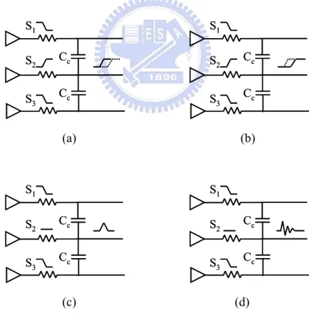
The result of crosstalk has implications on the data throughput and on signal integrity. In closely coupled interconnects such as in the long parallel interconnects, the affections of crosstalk include the speeded up signal or the considerable additional delay. The other different impacts are shown in Figure 2.4 [2].
Cc Cc S3 S2 S1 Cc Cc S3 S2 S1 Cc Cc S3 S2 S1 Cc Cc S3 S2 S1 (a) (b) Cc Cc S3 S2 S1 Cc Cc S3 S2 S1 Cc Cc S3 S2 S1 Cc Cc S3 S2 S1 (c) (d)
Figure 2.4 Crosstalk effects (a) additional delay (b) speedup (c) glitch (d) oscillation
2.4 Optimization for Minimum Delay
In general interconnect design, the repeater are optimally sized to minimize the interconnect delay. But these optimally sized repeaters are very large [3] (450 times the minimum sized inverter available in the correct technology for the global interconnects) and also dissipate a significant amount of power. The total power dissipation by such repeaters in high-performance designs is very high.
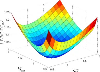
However, as shown in Figure 2.5, the interconnect delay is actually very low with respect to both the repeater size and interconnect length close to the minimum value [4]. S/Sopt l/lopt ( τ /l )/ ( τ /lop t ) S/Sopt l/lopt ( τ /l )/ ( τ /lop t )
Figure 2.5 Normalized delay per unit length as a function of repeater size and interconnect length
For the basic repeater model, it is shown in Figure 2.6. To obtain the optimal repeater size and the optimal interconnect length, we use the time constant of the repeater from Chapter 3. The delay per unit length of the repeater is given by
2 s s g d w w g w w r r 1 = (c +c )+ c + r c S + c r l l l S 2 τ × × . (2.6)
Therefore, the delay per unit length is optimized when 2 s g d opt w w r (c +c ) l = r c (2.7) s w opt w g r c S = r c . (2.8) Furthermore, the optimal delay per unit length is given by
d s g w w opt g c 1 = 2 r c r c 1+ 1+ l 2 c τ ⎛ ⎛ ⎞⎞ ⎛ ⎞ ⎜ ⎟ ⎜ ⎟ ⎜ ⎟ ⎜ ⎜ ⎟⎟ ⎝ ⎠ ⎝ ⎝ ⎠⎠. (2.9) ll
Figure 2.6 Basic repeater model
In a word, for the general interconnect design, we always find the optimal repeater size and the optimal interconnect length to minimize the interconnect delay.
2.5 Optimization for Power Dissipation
Because all global interconnects are not the critical path, a small delay penalty can be tolerated on these non-critical interconnects. There exists a potential for large power savings by using the smaller repeaters and the larger interconnect lengths.
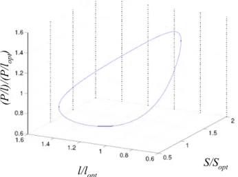
In the optimization for power consumption, the methodology is to estimate the repeater size and interconnect length which minimize the global interconnects power consumption for a given delay penalty. According to Figure 2.5, we fix a interconnect delay and obtain Figure 2.7. Figure 2.7 shows that we can use the optimal repeater size and the optimal interconnect length to obtain the optimal interconnect power for a given interconnect delay.
the total repeater power is not only the switching power, it also includes short-circuit power and leakage power. These powers are discussed particularly in Chapter 3.
S/Sopt l/lopt (P /l) /(P/ lopt ) S/Sopt l/lopt (P /l) /(P/ lopt )
Figure 2.7 Normalized power per unit length as a function of repeater size and interconnect length
The total repeater power is discussed in Chapter 3. The expression is
1 [( ) ] 2 3
repeater switching short-circuit leakage
d g w r P = P + P + P = k × c × + ×S c S + × + × × + ×c l k S t k S (2.10) Where min n min p 2 1 DD clk 3 3 2 DD t clk n ox min DD t clk 3 DD n off p off k = V f W 1 k = (V - 2V ) f = c ( ) (V - 2V ) f 12 L 12 1 k = V (W I +W I ) 2 β μ × × × × × × × . (2.11)
Therefore, for a given interconnect delay f , the repeater power is rewritten as
repeater 1 d g w 2 opt 3
P = k [(c S +c S)+c l] + k S (1+ f)( ) l + k S
l
τ
× × × × × × × × .(2.12)
Then, the repeater power per unit length is given by
repeater ' 1 d g w 2 3 P S S = k [ (c +c )+c ] + k S + k l × l × × . (2.13) l Where ' 2 2 opt k = k (1+ f)( ) l τ × (2.14)
We set the derivative of this with respect to S and l to zero. This equation is solved by using Newton-Raphson. Therefore, we can obtain the optimal repeater size and the optimal interconnect length to minimize the interconnect power consumption.
2.6 Summary
In this chapter, we discuss three effects of interconnect and two different optimizations for the global interconnects. These effects are considered to enhance our analysis in Chapter 3 and Chapter 4. Furthermore, according to two different optimizations, we improve them and propose a novel optimization to the global interconnects.
Chapter 3
Global Interconnects Circuit Design
3.1 Global Interconnects
The optimal repeater insertion is a good method to reduce power consumption and chip area. In Chapter 2, we have described various methodologies to optimize global interconnects. However, the methods are not enough to improve the performance completely. In this chapter, we introduce a novel methodology to optimize power and area effectively.
3.2 Model Parameter
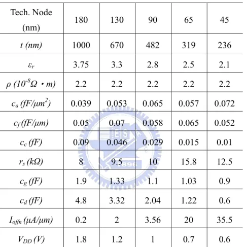
Before the optimization, we must acquire process parameters which affect the optimization. The technology parameters and equivalent circuit parameters are shown in Table 3.1. These parameters are obtained from the TSMC database and the
International Technology Roadmap for Semiconductors (ITRS) database. Where t is the interconnect thickness, εr is the dielectric constant, ρ is the metal resistivity, and V is the power supply voltage. DD
Table 3.1 also includes the input capacitance c , the output capacitance g c , and d output resistance r for a minimum sized inverter. s
Tech. Node (nm) 180 130 90 65 45 t (nm) 1000 670 482 319 236 εr 3.75 3.3 2.8 2.5 2.1 ρ (10-8Ω‧m) 2.2 2.2 2.2 2.2 2.2 ca (fF/μm2) 0.039 0.053 0.065 0.057 0.072 cf (fF/μm) 0.05 0.07 0.058 0.065 0.052 cc (fF) 0.09 0.046 0.029 0.015 0.01 rs (kΩ) 8 9.5 10 15.8 12.5 cg (fF) 1.9 1.33 1.1 1.03 0.9 cd (fF) 4.8 3.32 2.04 1.22 0.6 Ioffn (μA/μm) 0.2 2 3.56 20 35.5 VDD (V) 1.8 1.2 1 0.7 0.6
3.3 Model of Global Interconnects
Repeater Model
We use repeaters to relay the signal in the interconnect. The repeater model is presented in Figure 3.1. It consists of two minimum sized inverter and a segment of a metal wire. The repeater has an input capacitance of c , an output capacitance of g c , d and an output resistance of r . Therefore, for a repeater of size s S, the total input capacitance is Cg = × , the total output capacitance is S cg Cd = × , and the total S cd output resistance is Rtr =r Ss/ .
The interconnect is modeled as a distributed RC line. It contains the resistance per unit length r and capacitance per unit length w c . For an interconnect with w length l, the total resistance is Rw= × , and the total capacitance is l rw Cw= × . l cw
Cw Cd Cg Rtr Rw l Cd Cw Cg Rtr Rw Cw Cd Cg Rtr Rw l
Figure 3.1 Repeater RC model
On-chip Interconnect Model
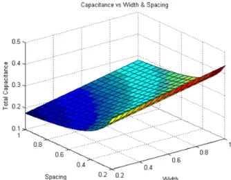
The cross section of global interconnects is shown in Figure 3.2, where W is the width. SP is the spacing. T is the thickness. c is the parallel plate a capacitance to the top and bottom layers of metals and is proportional to interconnect width. c is the fringing capacitance. f c is the coupling capacitance between the c neighboring interconnects and is inversely proportional to the interconnect spacing. The interconnect resistance per unit length is rw=ρ/Wt, where ρ is the metal resistivity.
W SP W SP W cc cf c a cf cc t W SP W SP W cc cf c a cf cc t
Figure 3.2 Cross section of global interconnects
According to TSMC 0.18μm technology, we can obtain c , a c , and f c c respectively. The interconnect capacitance per unit length c is w
c w a f c c = c W +c + SP × . (3.1) Furthermore, we can use MATLAB to plot the 3D graph for c as shown in w Figure 3.3.
Figure 3.3 Extracted capacitance cw as a function of width and spacing
for 180nm technology
3.4 Performance of Global Interconnects
Time Constant
After we obtain C , g C , d R , tr C , and w R from Section 3.3, the time w τ constant of the repeater model is [3]
2 s s g d w w g w w r r 1 = (c S +c S)+ c l + r l c S + c r l S S 2 τ × × . (3.2)
Bandwidth
The data transmitted in a single interconnect with bandwidth of BWsingle is inversely proportional to the time constant. To acquire the voltage swing from 5% of
DD
V to 95% of V , the bandwidth of a single interconnect DD BWsingle is defined as single 2 s s g d w w g w w 1 1 BW = = r r 1 3.32 (c S + c S) + c l + r l c S + c r l 3.32 S S 2 τ× ⎛ × × ⎞× ⎜ ⎟ ⎝ ⎠ . (3.3)
The global interconnects with repeater insertion is shown in Figure 3.4, where L is the total interconnect length. The global interconnects which link many blocks of a SOC usually consist of a large number (n) of the parallel interconnects, and the total bandwidth BWtotal is
total single 1 BW = n BW = n 3.32 τ × × × . (3.4)
…
l L…
…
…
l L…
…
Figure 3.4 Global interconnects with repeater insertion
Power
With technology scaling, the total power consumption is not only the switching power. The leakage power increases rapidly and the short-circuit power has also been shown to be a significant fraction (up to 15%) of the total power consumption for low-power and high-speed designs [4]. The three components of the total power are
analyzed as follows.
Switching power mode
The switching power of the repeater is shown in Figure 3.5. The switching power occurs when current in the repeater charge or discharge C , g C , and w C . The d expression of switching power is
2 switching d g w DD clk 2 d g w DD clk P = [(c S +c S)+c l] V f = (C +C +C ) V f × × × × × × × . (3.5)
Where VDD is power supply, fclk is clock frequency, C is the wire w capacitance, C is the input capacitance, and g C is the output capacitance. d
Cw l Cg Cd Cw l Cg Cd
Figure 3.5 Switching power model of repeater
Short-circuit power mode
The short-circuit power of the repeater is shown in Figure 3.6(a). The short-circuit power occurs during the transition from either high-to-low or low-to-high. Both NMOS and PMOS transistors are on for a short period of time, and there is a current drawn from V through the two transistors to the ground [5]. The input and DD output voltage and current waveforms are shown in Figure 3.6(b). We denote t the r time for the input to rise from V to tn VDD −Vtp. The short-circuit current waveform is approximated by a triangular wave [4]. The expression of short-circuit power is
2 3 2 1 2 1 t t t 2 short-circuit t t DD t in t 3 r 3 DD t DD t r clk p 1 1 4 P = 2 [ I(t)dt + I(t)dt] V = (V (t)-V ) dt T T T 2 t = (V - 2V ) = (V - 2V ) t f 12 t 12 β β β × × × ×
∫
∫
∫
. (3.6)Vin Vout Isc Vin Vout Isc (a) (b)
Figure 3.6 Voltage and current waveforms of a CMOS inverter
Leakage power mode
For a long interconnect, we assume that there are half ones and half zeros. When inverter has an input of one, the NMOS transistor is turned ON. The leakage current is determined by the PMOS transistor. When inverter has an input of zero, the PMOS transistor is turned ON. The leakage current is determined by the NMOS transistor. The expression of leakage power is
n p
min n min p
leakage DD leakage DD n off p off
DD n off p off P = V I = 0.5 V (W I +W I ) = 0.5 V (W I +W I ) S × × × . (3.7) leakage
I is the leakage current flowing through the repeater. Ioffn (Ioffp) is the leakage current per unit NMOS (PMOS) transistor width. W (n W ) is the width of p the NMOS (PMOS). Wnmin (Wpmin) is the width of the NMOS (PMOS) transistor in minimum sized inverter.
These three types of power constitute the power dissipation in one stage.
Prepeater= Pswitching +Pshort circuit− +Pleakage. (3.8)
Imax Vtn VDD-VVDDtp tr tf T t1t2t3 Time Time VIN ISC Imax Vtn VDD-VVDDtp tr tf T t1t2t3 Time Time VIN ISC
The total power for the global interconnects with repeater insertion is shown in Figure 3.4. In order to analyze the total power simply, we consider merely about
switching
P that is up to 85% of total power. The expression of total power Ptotal is
bw f = 2 , (3.9) w g d L L C = (c l) +(c S + c S) l l × × × × × , (3.10) 2 2 single dd w g d dd L L P = f C V = f [(c l) +(c S +c S) ] V l l × × × × × × × × × , (3.11) 2 total dd total 1 2 total w g d dd 1 P = n (f C V )= n f energy = BW p 2 1 L = BW [c L+(c S + c S) ] V 2 l × × × × × × × × × × × × × × . (3.12)
Where f is the frequency of the transmitted data, C is the total capacitance of the global interconnects, p is the energy dissipation of the single interconnect. 1
Area
The area of a single interconnect Asingle is shown in Figure 3.7. After we obtain the width and spacing of the interconnect, the area of a single interconnect Asingle is
single
L A = (W + SP) l
l
× × . (3.13) We implement the overall chip in Figure 3.4 and put the repeaters under the global interconnects. Therefore, we only consider the area of the global interconnects. The expression of total area Atotal is
total total BW L A = n (W + SP) l = (W + SP) L l bw × × × × × . (3.14)
…
L…
SP W…
L…
SP WFigure 3.7 Area of a single interconnect with repeater insertion
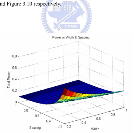
Summary of Performance
According to the previous discussion, we observe that the bandwidth, power, and area of a single interconnect are affected by the interconnect width and spacing. Furthermore, BWtotal , Ptotal , and Atotal are proportional to BWsingle, Psingle , and
single
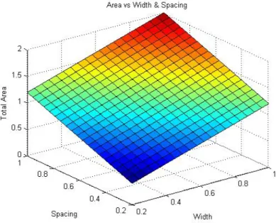
A respectively. Therefore, we use MATLAB to plot 3D graph for BWtotal, Ptotal, and Atotal as function of width and spacing. These 3D graph are shown in Figure 3.8, Figure 3.9, and Figure 3.10 respectively.
Figure 3.9 MATLAB simulation for bandwidth vs. width and spacing
Figure 3.10 MATLAB simulation for area vs. width and spacing
3.5 Figure of Merit for Optimization
The aim of global interconnects design is to obtain large bandwidth,small global interconnects area, and low power consumption simultaneously. According to the summary of performance discussed in Section 3.4, the large bandwidth BWsingle
requiressmall interconnect width and spacing. But the low power consumption Psingle and the small interconnect area Asingle require large interconnect width and spacing.
The global interconnects width and spacing affect the overall chip performance such as the bandwidth, the power consumption, and the interconnect area. The tradeoff between the bandwidth, the power, and the area is needed. Therefore, the figure of merit FOM is used for the global interconnects. It considers for the bandwidth, power consumption, and area simultaneously. The expression of FOM is
total total total
BW FOM =
P ×A . (3.15)
The proposed novel methodology is to optimize the global interconnects and obtain the maximal FOM simultaneously for the various technologies. The proposed methodology considers three parts for the global interconnects, 1) the optimal interconnect width and spacing, 2) the optimal repeater size and interconnect length, 3) the optimal interconnect bandwidth.
Optimal Global Interconnects Width and Spacing
The previous equation is determined by the various interconnect width and spacing. The optimal interconnect width and spacing are not calculated. In this section, we use (3.11) and (3.13) to obtain the product of power and area for a single interconnect. The expression is
2 single single w g d dd L P A = {f[c L+(c S +c S) ] V } [(W + SP) L] l × × × × × × × × × . (3.16)
Minimum power mode
The minimum power for the single interconnect is while the interconnect spacing is to tend towards infinite. When the spacing increases, the capacitance reduces. We define the infinite interconnect spacing as when the parallel plate capacitance is 10
times the coupling capacitance. Therefore, we substitute the minimum interconnect width to (3.16). c a c c W 10 SP × ≥ × . (3.17) c a 10c SP c W ≥ × . (3.18)
Minimum area mode
Minimum area for the single interconnect is while the interconnect width and spacing are the smallest.
Minimum product of power and area mode
We can increase the interconnect spacing to reduce the power of the single interconnect. But, it also increases the area. Therefore, the minimum product of power and area mode is an important issue for the whole performance. In this section, we simplify (3.16) to single single w P ×A ∝ ×K [c ×(W + SP)] (3.19) 2 DD K = × ×f L V . (3.20) To achieve the minimum product of power and area mode, the interconnect width must be minimum. On this premise, the optimal interconnect spacing is calculated by setting the derivative of Psingle×Asingle on SP to be zero.
(Psingle Asingle)= 0 SP
∂ ×
∂ (3.21) We solve (3.21) and the optimal interconnect spacing is
c opt a f c W SP = c W +c × × . (3.22)
Use (3.16) and the technology parameter of TSMC 0.18μm, we can use MATLAB to plot 2D graph in Figure 3.11 for Psingle×Asingle versus to the various spacing.
Figure 3.11 MATLAB simulation for product of power and area vs. minimal width and spacing
Optimal Repeater Size and Optimal Interconnect Length
After we obtain the optimal interconnect width and spacing, we substitute (3.4),(3.12), and (3.14) to (3.15). The FOM is written as
total total total total total total 2 total dd BW BW FOM = = BW 1 P A ( BW energy) [ (W + SP) L] 2 bw 2 1 = 3.32 BW V L (W + SP) c 1 K c τ τ × × × × × × × × × × × × ∝ × × . (3.23)
We observe that the FOM is inversely proportional to the product of time constant and capacitance τ×c. The expression is
2 s s g d w w g w w w g d r r 1 1 c = (c S + c S) + c l + r l c S + c r l c +(c +c ) S S 2 l τ× ⎛⎜ × × ⎞ ⎛⎟×⎜ × ⎞⎟ ⎝ ⎠ ⎝ ⎠ (3.24)
The optimal repeater size is obtained by setting the derivative of τ×c on S to be zero. c = 0 S τ ∂ × ∂ (3.25) We solve (3.25) and the optimal repeater size is
s w opt w g r c S = r c . (3.26) We substitute (3.3), (3.26), and the optimal interconnect width and spacing to HSPICE. The simulations are shown in Figure 3.12 and Figure 3.13. The Figure 3.12 expresses that the interconnect bandwidth is versus to the interconnect length. Figure 3.13 expresses that the interconnect bandwidth per energy is versus to the interconnect length. VDD = 1.8V 5.00E+08 1.00E+09 1.50E+09 2.00E+09 2.50E+09 3.00E+09 3.50E+09 4.00E+09 4.50E+09 0 10 20 30 40 50
Number of repeaters per cm
Ba nd w id th HSPICE Simulation
VDD = 1.8V 1.00E+07 3.00E+07 5.00E+07 7.00E+07 9.00E+07 1.10E+08 1.30E+08 1.50E+08 0 10 20 30 40 50
Number of repeaters per cm
ba ndwi dth pe r bi t-en er gy ( bps /pJ )
Figure 3.13 Variation of bandwidth per energy with number of repeaters
The optimal interconnect length is obtained by setting the derivative of τ×c on
l to be zero. c = 0 l τ ∂ × ∂ (3.27) We solve (3.27) and the optimal repeater size is
s g opt w w 0.7r c l = r c . (3.28) Therefore, we substitute (3.3), (3.26), (3.28), and the optimal interconnect width and spacing to HSPICE again. The simulation is shown in Figure 3.14. We obtain the maximum value of interconnect bandwidth per energy. Therefore, we claim that the interconnect circuit is optimized.
VDD = 1.8V 1.00E+07 3.00E+07 5.00E+07 7.00E+07 9.00E+07 1.10E+08 1.30E+08 1.50E+08 0 10 20 30 40 50
Number of repeaters per cm
ba nd w idth pe r bit-en er gy ( bps /pJ )
Figure 3.14 Variation of bandwidth per energy with number of repeaters
Optimal Interconnect Bandwidth
After we obtain the optimal interconnect width and spacing, the optimal repeater size, and the optimal interconnect length, we substitute them to (3.3) and obtain the optimal interconnect bandwidth. The expression of the optimal interconnect bandwidth is
(
)
opt s g s d 1 1 BW = = 3.32 3r c + r c 3.32 τ× × . (3.29)3.6 Optimization Flow
The optimization flow for the global interconnects is shown in Figure 3.12. It includes three methods, 1) the optimization for the minimum product of power and area mode, 2) the optimization for the minimum area mode, 3) the optimization for the minimal power mode.
Figure 3.15 Optimization flow for global interconnects To choose the optimization for minimal power To choose the optimization for minimal area Begin Design To choose process technology Optimization END Decide the optimal interconnect Width (Wopt) and Spacing (SPopt)
Decide the optimal Repeater Size (Sopt) and Interconnect Length (lopt)
Decide the optimal bandwidth (BWopt) of the interconnect
Precise Ca , Cf , Cc Precise cw , rw Precise rs , cg To choose the optimization for minimal product of
3.7 Optimal Design Parameter
According to optimization flow, we optimize the minimum product of power and area to obtain the maximum FOM. Table 3.2 shows the optimal design expression of the global interconnects.
Parameter Optimal design
Interconnect Space (Wopt) Minimum Width
Interconnect Space (SPopt)
c opt a f c W SP = c W +c × × Repeater Size (Sopt)
s w opt w g r c S = r c Interconnect length (lopt)
s g opt w w 0.7r c l = r c Interconnect bandwidth (BWopt)
(
)
opt s g s d 1 BW = 3r c + r c ×3.32 Table 3.2 Optimal design expressionWe substitute the model parameter to the previous equation and calculate the optimal design parameters are shown in Table 3.3.
Supply voltage - repeaters 1.8V , 13 repeaters/cm Interconnect dimensions W = 0.28μm , SP = 0.64μm
Repeater dimensions Wn = 9.9μm , Wp = 35.2μm
Bandwidth 3Gbps
Total power 9.2mW
Total area 9200μm2
3.8 Summary
In this chapter, we improve the optimization for the global interconnects. The optimal design flow is proposed. We optimize the interconnect width and spacing, the repeater size and interconnect length, and the interconnect bandwidth. Finally, according to the optimal design parameter, we claim that the interconnect circuit is optimized.
Chapter 4
Global Interconnects Circuit
Implementation
4.1 Single Interconnect Structure
Figure 4.1 is the typical single interconnect. According to the optimal design value, the data rate is 3Gbps and the interconnect length L is 10000μm. Figure 4.2 shows the pre-simulation results of the last repeater output. Table 4.1 shows the total power consumption and jitter of the single interconnect.
…
l L…
l L1.8 1.6 1.4 1.2 1 0.8 0.6 0.4 0.2 0 0 200p 400p 600p 1.8 1.6 1.4 1.2 1 0.8 0.6 0.4 0.2 0 0 200p 400p 600p 1.8 1.6 1.4 1.2 1 0.8 0.6 0.4 0.2 0 0 200p 400p 600p 1.8 1.6 1.4 1.2 1 0.8 0.6 0.4 0.2 0 0 200p 400p 600p (a) TT (b) SS 1.8 1.6 1.4 1.2 1 0.8 0.6 0.4 0.2 0 0 200p 400p 600p 1.8 1.6 1.4 1.2 1 0.8 0.6 0.4 0.2 0 0 200p 400p 600p 1.8 1.6 1.4 1.2 1 0.8 0.6 0.4 0.2 0 0 200p 400p 600p 1.8 1.6 1.4 1.2 1 0.8 0.6 0.4 0.2 0 0 200p 400p 600p (c) FF (d) SF 1.8 1.6 1.4 1.2 1 0.8 0.6 0.4 0.2 0 0 200p 400p 600p 1.8 1.6 1.4 1.2 1 0.8 0.6 0.4 0.2 0 0 200p 400p 600p (e) FS
Figure 4.2 Corners of the single interconnect
L = 10000μm TT SS FF SF FS
Power 8.1mW 7.5mW 9.1mW 8mW 82mW
Jitter(p-p) 43ps 63ps 35.6ps 43.8ps 44.5ps
4.2 Global Interconnects Structure
Typical global interconnects implementation
Figure 4.3 is the typical layout of unidirectional global interconnects. Figure 4.4 shows the coupling effect of crosstalk by considering a simple case of three parallel lines with the optimal repeaters as drivers. In general, the length capacitor is inversely proportional to the interconnect spacing and proportional to the interconnect length that runs in parallel model. The cross coupling capacitor C is in the c horizontal spacing between the global interconnects.
…
…
…
…
…
…
Figure 4.3 Unidirectional global interconnects
…
Cs Rw Cc Cs Rw Cc Cs Rw Cs Rw Cc Cs Rw Cc Cs Rw…
…
…
Cs Rw Cc Cs Rw Cc Cs Rw Cs Rw Cc Cs Rw Cc Cs Rw Cs Rw Cc Cs Rw Cc Cs Rw Cs Rw Cc Cs Rw Cc Cs Rw Cs Rw Cc Cs Rw Cc Cs Rw Cs Rw Cc Cs Rw Cc Cs Rw…
…
Figure 4.4 Geometrical RC model of the parallel interconnect
On-chip global interconnects implementation
To reduce the impact of capacitive coupling noise, we use the interleaved repeaters for the global interconnects which is described in [11]. The layout structure is shown in Figure 4.5.
This approach uses the offset repeaters in a bus-like structure to minimize the impact of coupling capacitance on delay and crosstalk noise. If the repeaters are offset so that each gate is placed in the middle of its neighboring gates, the affection is limited to one. This is because potential worst-case simultaneous switching on adjacent wires can be present for only half the impacted line’s length. In such condition the other half of the impacted line will consequently experience best-case neighboring switching activity. The Figure 4.6 shows the impact of the interleaved repeaters.
…
…
…
…
…
…
Figure 4.5 Layout of on-chip global interconnects
4.3 Generation of Random Data
In order to test the global interconnects independently, we put a data generator to connect the global interconnects. It is difficult to generate completely random binary data because for the randomness to manifest itself. For this reason, it is common to employ a PRBS. It is “pseudo” because it is deterministic and after 2 -1 elements it n starts to repeat itself. It is the unlike real random sequence.
Due to the data rate operating at gigahertz, we choose the dynamic DFF to setup the PRBS. The dynamic DFF is shown in Figure 4.7. In Figure 4.8, there are twelve resettable dynamic DFFs and an XOR gate to send the result to the input of the first DFF.
D Q
Reset Reset
D Q
Reset Reset
Figure 4.7 Resettable dynamic DFF
D D QQ
…
D0 D1 D4 D5 D6 D7 D11 D5 Clk Q Q D D DD QQ QQ Q Q Q Q Q Q Q Q D D D D D D D D D D…
D11 D0 D10 D D QQ…
D0 D1 D4 D5 D6 D7 D11 D5 Clk Q Q D D DD QQ QQ Q Q Q Q Q Q Q Q D D D D D D D D D D…
D11 D0 D11 D0 D10A segment of 212− data patterns is generated with twelve registers and an 1 XOR circuit. The property of the PRBS architecture is that it can generate all possible combination patterns except the all zero vector. The probability of transitions from 0 to 1 and 1 to 0 are the same as 50%. It is a simple and regular structure. This technique can be extended to an m-bit system so as to produce a sequence of length
2m− . 1
Figure 4.9 shows the HSPICE simulation results and Figure 4.10 shows the eye diagrams of PRBS. 1 0 2 1 0 2 1 0 2 1 0 2 1 0 2 1 0 2 1 0 2 20n 40n 60n 1 0 2 1 0 2 1 0 2 1 0 2 1 0 2 1 0 2 1 0 2 20n 40n 60n
Figure 4.9 Timing diagram of PRBS
1 0 2 1 0 2 1 0 2 1 0 2 1 0 2 1 0 2 1 0 2 0 200p 400p 600p 1 0 2 1 0 2 1 0 2 1 0 2 1 0 2 1 0 2 1 0 2 0 200p 400p 600p
4.4 Output Buffer
When the data exports to the chip, they are distorted. Because the boning wire and pad cause the resonance of inductance and capacitance. Therefore, output buffer plays an important role to transmit signals. The output data stream usually has large jitter and small amplitude swing. Therefore, the output sensitivity, symmetry, and bandwidth are major concerns.
Figure 4.11 shows the architecture of output buffer. The proposed architecture is all digitized. It operates in fully differential and amplifies the swing of the output signal stage by stage. We use two inverters which connect input to output by each other to make hysteresis. It makes the signal transfer with symmetry and reduces the effect of noise. The inverter connected with a transmission gate has two advantages. First, the inverter which input and output connect together makes the input common-mode at0.5V . We don’t need common-mode feed back circuit. Second, DD the transmission gate act as resister and it makes the inductive peaking effect.
Although we reduce the gain, we extend the bandwidth of the inverter. In order to reach the large swing of output, we need more stages to reach it.
in inb A B C D in inb A B C D
4.5 Layout and Simulation
The proposed 10mm optimal global interconnects is implemented by National Chip Implement Center (CIC) in TSMC 0.18μm 1P6M CMOS process. The data rate is 3Gbps per channel. The layout of this chip is shown in Figure 4.12. The core area is
2
0 196. mm (700um×280um) and the total area is 0.6144mm (2 960um×640um). The chip includes a 10mm global interconnects, a PRBS, and an output buffer. The rest area is filled up with decouple capacitors to bypass power noise. The chip will be implemented and send back in January 2008.
10mm on-chip global interconnect with Repeater chain
Decouple Cap Buffer PRBS 960μm 640 μ m
10mm on-chip global interconnect with Repeater chain
Decouple Cap Buffer PRBS 960μm 640 μ m
Figure 4.12 Layout of 10mm optimal global interconnects
We input 3Gbps PRBS signal to test the 10mm optimal global interconnects. Figure 4.13 and Figure 4.14 show the five corners of the last repeater outputs for the 5mm optimized global interconnects and the 10mm optimized global interconnects respectively. These simulations are all post layout-simulation results.
1.8 1.6 1.4 1.2 1 0.8 0.6 0.4 0.2 0 0 200p 400p 600p 1.8 1.6 1.4 1.2 1 0.8 0.6 0.4 0.2 0 0 200p 400p 600p 1.8 1.6 1.4 1.2 1 0.8 0.6 0.4 0.2 0 0 200p 400p 600p 1.8 1.6 1.4 1.2 1 0.8 0.6 0.4 0.2 0 0 200p 400p 600p (a) TT (b) SS 1.8 1.6 1.4 1.2 1 0.8 0.6 0.4 0.2 0 0 200p 400p 600p 1.8 1.6 1.4 1.2 1 0.8 0.6 0.4 0.2 0 0 200p 400p 600p 1.8 1.6 1.4 1.2 1 0.8 0.6 0.4 0.2 0 0 200p 400p 600p 1.8 1.6 1.4 1.2 1 0.8 0.6 0.4 0.2 0 0 200p 400p 600p (c) FF (d) SF 1.8 1.6 1.4 1.2 1 0.8 0.6 0.4 0.2 0 0 200p 400p 600p 1.8 1.6 1.4 1.2 1 0.8 0.6 0.4 0.2 0 0 200p 400p 600p (e) FS
Figure 4.13 Corners of the global interconnects for 5000μm
L = 5000μm TT SS FF SF FS
Jitter(p-p) 23.9ps 24.5ps 33ps 25ps 24.4ps
1.8 1.6 1.4 1.2 1 0.8 0.6 0.4 0.2 0 0 200p 400p 600p 1.8 1.6 1.4 1.2 1 0.8 0.6 0.4 0.2 0 0 200p 400p 600p 1.8 1.6 1.4 1.2 1 0.8 0.6 0.4 0.2 0 0 200p 400p 600p 1.8 1.6 1.4 1.2 1 0.8 0.6 0.4 0.2 0 0 200p 400p 600p (a) TT (b) SS 1.8 1.6 1.4 1.2 1 0.8 0.6 0.4 0.2 0 0 200p 400p 600p 1.8 1.6 1.4 1.2 1 0.8 0.6 0.4 0.2 0 0 200p 400p 600p 1.8 1.6 1.4 1.2 1 0.8 0.6 0.4 0.2 0 0 200p 400p 600p 1.8 1.6 1.4 1.2 1 0.8 0.6 0.4 0.2 0 0 200p 400p 600p (c) FF (d) SF 1.8 1.6 1.4 1.2 1 0.8 0.6 0.4 0.2 0 0 200p 400p 600p 1.8 1.6 1.4 1.2 1 0.8 0.6 0.4 0.2 0 0 200p 400p 600p (e) FS
Figure 4.14 Corners of the global interconnects for 10000μm
L = 10000μm TT SS FF SF FS
Power 85.6mW 82mW 90mW 85.5mW 85.9mW
Jitter(p-p) 41.4ps 44.1ps 41.9ps 41.7ps 44ps
Besides, we scale down the power supply to 1V. The data rate is down to 2.2Gbps. Figure 4.15 shows the eye diagram of global interconnects. The jitter is 53.9ps and the power consumption is 2.475mW.
0 200p 400p 600p 800p 1 0.8 0.6 0.2 0 0.4 0 200p 400p 600p 800p 1 0.8 0.6 0.2 0 0.4
We also change the temperature condition test the 10mm optimal global interconnects. Figure 4.16 and Figure 4.17 show the affections of temperature variation respectively. 0 200p 400p 600p 1.8 1.6 1.4 1.2 1 0.8 0.6 0.2 0 0.4 0 200p 400p 600p 1.8 1.6 1.4 1.2 1 0.8 0.6 0.2 0 0.4
Figure 4.16 Temperature = 0 for the global interconnects
0 200p 400p 600p 1.8 1.6 1.4 1.2 1 0.8 0.6 0.2 0 0.4 0 200p 400p 600p 1.8 1.6 1.4 1.2 1 0.8 0.6 0.2 0 0.4
The post layout-simulation summaries are shown in Table 4.2 and Table 4.3 respectively. The best interconnect has at least 0.87 unit interval (UI) eye-opening of 333ps period at the end of last repeater output. Table 4.4 shows the summary of the 10mm global interconnects.
Item Specification Process TSMC 0.18μm 1P6M
Supply Voltage 1.8V
Data Rate 3Gbps/channel × 8
Link 10mm on chip micro-strip line Jitter of received data (pk-to-pk) 41.4ps (0.124UI)
Repeater chain Layout Area 700μm × 280μm
Core Layout Area 960μm × 640μm
PRBS Generator 4mW Repeater Chain 73.6mW(9.2mW × 8) Output Buffer 8mW Power Consumption Total 85.6mW
Table 4.4 Summary of the 10mm global interconnects
4.6 Performance Comparison
The specifications of the global interconnects are shown in Table 4.5. For the performances of the global interconnects, we concern mainly about the bandwidth, the power consumption, the interconnect length, and the area of the global interconnects. These important performances are substituted to (3.15) to calculate FOM.
Besides, for the convenience of comparison at the same level, we scale down the power supply to 1V and obtain 2.475mW power consumption at 2.2Gbps.
Reference Bandwidth Process Supply Power Link Area JSSC’06[13] 1Gbps 0.35μm 2.5V 5.8mW 1.75cm 0.105mm2 TVLSI’05[14] 1.47Gbps 0.18μm 2V 14.2mW 1cm 0.005mm2 ISQED’05[15] 1.66Gbps 0.18μm 1V 3.1mW 1cm 0.006mm2 JSSC’03[16] 2Gbps 0.18μm 1.8V 30mW 2cm 0.018mm2 ASSCC’05[18] 2.5Gbps 0.13μm 1.2V 4.6mW 0.9cm 0.0108mm2 3Gbps 0.18μm 1.8V 9.2mW 1cm 0.0092mm2 This work 2.2Gbps 0.18μm 1V 2.47mW 1cm 0.0092mm2
Table 4.5 Specifications of the global interconnects
The maximum FOM and the minimum power consumption per bit are important targets for the global interconnects. They are shown in Table 4.6. The proposed architecture’s FOM is maximum when the power supply is 1.8V. Furthermore, we also scale down the power supply to 1V. The FOM is still better than other cases.
In high-speed link design, the power consumption per bit is usually used to determine the performance. In Table 4.6, we obtain the minimum power consumption per bit when the power supplies are 1V and 1.8V respectively.
Reference FOM Power/bit (pJ/bit)
JSSC’06[13] 1.6 5.8 TVLSI’05[14] 20 6.55 ISQED’05[15] 89 1.86 JSSC’03[16] 3.7 8 ASSCC’05[18] 50 1.84 35 3.06 This work 97 1.13 Table 4.6 Comparisons of the global interconnects
4.7 Measurement Considerations
The test configuration is shown in Figure 4.15 and we illustrate the purpose of each instrument. Power supply enables this chip. Agilent N4901B Serial BERT provides input up to 3Gbps data rate and the 3GHz differential clock. By a wide-band oscilloscope, we can observe the high-speed performance of the global interconnects. We expect to obtain 3Gbps signal from the output of the last repeater and the eye-opening diagram which is up to 0.85UI.
Besides, we will regulate the power supply voltage to obtain the various optimal bandwidths. The power is measured by Ktythley 2400 Source Meter. According to the bandwidth and the power, we also calculate the FOM of this chip.
Ktythley:2400 source meter power measurement Ktythley:2400 source meter
power measurement Power measurement N4901B Serial BERT 13.5 Gb/s N4901B Serial BERT 13.5 Gb/s BER measurement
HP E3610A DC Power Supply Output Buffer HP E3610A DC Power Supply
Output Buffer Agilent 86100B Wide-Bandwidth Oscilloscope Agilent 86100B Wide-Bandwidth Oscilloscope Jitter measurement
HP E3610A DC Power Supply RRBS / Repeater chain HP E3610A DC Power Supply
RRBS / Repeater chain PCB Din / CLK / CLKB VDD3 / GND3 VDD1 / GND1 VDD2 / GND2 Vout 3 / Vout 7
4.8 Summary
In this chapter, the 10mm on-chip global interconnects are optimized by the proposed methodology. It is implemented by TSMC 0.18μm 1P6M technology. The data rate is 3Gbps. The power consumption is 9.2mW per interconnect. The power per bit is 3.06 pJ/bit. Besides, our implementation is considered to reduce the crosstalk effect. It increases the accuracy of signal.
Chapter 5
Conclusion
5.1 Conclusion
This thesis presents a novel method to optimize the global interconnects in SOC. According to the paper survey, the global interconnects optimizations are not complete yet. In the proposed optimal methodology, the global interconnects width and spacing, the repeater size and the interconnect length, and the interconnect bandwidth are optimized simultaneously. Furthermore, the minimum product of power and area is optimized, so this optimization maximizes the FOM.
This thesis provides a more complete optimization. Therefore, this thesis achieves the data rate of 3Gbps, the single interconnect power consumption of 9.2mW, and the transmitted distance of 10mm. The power per bit is 3.06 pJ/bit. We also scale down the power supply to 1V. The data rate is 2.2Gbps and the single interconnect power consumption of 2.475mW. The power per bit is 1.125 pJ/bit.
5.2 Future Work
The optimization is established for the global interconnects. The unidirectional interconnect is not a sole choose. For the request of SOC, we modify the optimization slightly. The signal is transmitted and received from any segment of global interconnects. The global interconnects are used more efficiently.
Bibliography
[1] Neil H. E. Weste and David Harrris, A Circuits and Systems perspective, Third Edition.
[2] Xiaoliang Bai and Sujit Dey “High-Level Crosstalk Defect Simulation Methodology for System-on-Chip Interconnects’’ IEEE TRANSACTIONS ON COMPUTER-AIDED DESIGN OF INTEGRATED CIRCUITS AND SYSTEMS, VOL. 23, NO. 9, SEPTEMBER 2004
[3] H. B. Bakoglu, Circuits, Interconnections and Packaging for VLSI. Addision-Wesley,1990.
[4] Kaustav Banerjee, Member, IEEE, and Amit Mehrotra, Member, IEEE “A Power-Optimal Repeater Insertion Methodology for Global Interconnects in
Nanometer Designs” IEEE TRANSACTIONS ON ELECTRON DEVICES, VOL.
49, NO. 11, NOVEMBER 2002
[5] Wei Jin, Philip C. H. Chan, Senior Member, IEEE, and Mansun Chan, Member, IEEE “On the Power Dissipation in Dynamic Threshold Silicon-on-Insulator
CMOS Inverter” IEEE TRANSACTIONS ON ELECTRON DEVICES, VOL. 45,
NO. 8, AUGUST 1998
[6] Man Lung Mui, Kaustav Banerjee, Senior Member, IEEE, and Amit Mehrotra, Member, IEEE “A Global Interconnect Optimization Scheme for Nanometer Scale VLSI With Implications for Latency, Bandwidth, and Power Dissipation” IEEE TRANSACTIONS ON ELECTRON DEVICES, VOL. 51, NO. 2, FEBRUARY 2004
[7] K. Banerjee, A. Mehrotra, A. Sangiovanni-Vincentelli, and C. Hu, “On thermal effects in deep submicron VLSI interconnects,” in Proc. Design Automation Conf., 1999, pp. 885–891.
[8] Xiao-Chun Li, Jun-Fa Mao, Senior Member, IEEE, Hui-Fen Huang, and Ye Liu “Global Interconnect Width and Spacing Optimization for Latency, Bandwidth
and Power Dissipation” IEEE TRANSACTIONS ON ELECTRON DEVICES,
VOL. 52, NO. 10, OCTOBER 2005
[9] Min Tang and Jun-Fa Mao “Optimization of Global Interconnects in High Performance VLSI Circuits” Proceedings of the 19th International Conference on VLSI Design (VLSID’06)
[10] HARRY J. M. VEENDRICK “Short-Circuit Dissipation of Static CMOS Circuitry and Its Impact on the Design of Buffer Circuits” IEEE JOURNAL OF SOLID-STATE CIRCUITS, VOL. SC-19, NO. 4, AUGUST 1984
[11] A.B. Kahng, S. Muddu and E. Sarto, “Tuning Strategies for Global Interconnects in High-Performance Deep Submicron IC’s’’ VLSI Design 10(1), 1999, pp.21-34