國 立 交 通 大 學
電子工程學系 電子研究所
碩 士 論 文
一個與電壓控制震盪器整合的
一個與電壓控制震盪器整合的
一個與電壓控制震盪器整合的
一個與電壓控制震盪器整合的 K 頻帶互補式金
頻帶互補式金
頻帶互補式金
頻帶互補式金
氧半
氧半
氧半
氧半 E 類功率放大器
類功率放大器
類功率放大器
類功率放大器
A K-Band CMOS Class E Power Amplifier
Integrated with Voltage-Controlled Oscillator
研 究 生: 彭國權 (Guo-Quan Peng)
指導教授: 吳重雨教授 (Prof. Chung-Yu Wu)
一個與電壓控制震盪器整合的
一個與電壓控制震盪器整合的
一個與電壓控制震盪器整合的
一個與電壓控制震盪器整合的 K 頻帶互補式金氧半
頻帶互補式金氧半
頻帶互補式金氧半
頻帶互補式金氧半
E 類功
類功
類功率放大器
類功
率放大器
率放大器
率放大器
A K-Band CMOS Class E Power Amplifier
Integrated with Voltage-Controlled Oscillator
研 究 生:彭國權
Student: Guo-Quan Peng
指導教授:吳重雨教授
Advisor: Prof. Chung-Yu Wu
國立交通大學
電子工程學系
電子研究所
碩士論文
A Thesis
Submitted to Department of Electronics Engineering and Institute of Electronics
College of Electrical and Computer Engineering
National Chiao-Tung University
in Partial Fulfillment of the Requirements
for the Degree of
Master
in
Electronics Engineering
November 2010
Hsin-Chu, Taiwan, Republic of China
一個與電壓控制震盪器整合的
一個與電壓控制震盪器整合的
一個與電壓控制震盪器整合的
一個與電壓控制震盪器整合的 K 頻帶互補
頻帶互補
頻帶互補
頻帶互補
式金氧半
式金氧半
式金氧半
式金氧半 E 類功率放大器
類功率放大器
類功率放大器
類功率放大器
研究生
研究生
研究生
研究生: 彭國權
彭國權
彭國權
彭國權
指導教授
指導教授
指導教授
指導教授: 吳重雨
吳重雨
吳重雨 博士
吳重雨
博士
博士
博士
國立交通大學
國立交通大學
國立交通大學
國立交通大學
電子工程學系
電子工程學系
電子工程學系
電子工程學系 電子研究所碩士班
電子研究所碩士班
電子研究所碩士班
電子研究所碩士班
摘要
摘要
摘要
摘要
具有高操作頻 具有高操作頻 具有高操作頻 具有高操作頻率高傳輸速率的通訊系統已被視為次世代通訊系統的主軸率高傳輸速率的通訊系統已被視為次世代通訊系統的主軸率高傳輸速率的通訊系統已被視為次世代通訊系統的主軸率高傳輸速率的通訊系統已被視為次世代通訊系統的主軸。。。。在最近在最近在最近在最近 幾年 幾年 幾年 幾年,,,,K 頻帶頻帶頻帶頻帶中中中中,,,,已已有已已有有許多頻帶如有許多頻帶如許多頻帶如 24.05–24.25-GHz 的許多頻帶如 的 ISM-band 及的的 及及 22–29 GHz 被及 被被被 FCC 釋出作為汽車雷達應用等用途釋出作為汽車雷達應用等用途釋出作為汽車雷達應用等用途釋出作為汽車雷達應用等用途。。。 。 此論文中介紹 此論文中介紹 此論文中介紹 此論文中介紹實現一個實現一個實現一個實現一個與電壓控制震盪器整合與電壓控制震盪器整合與電壓控制震盪器整合與電壓控制震盪器整合操作在操作在操作在操作在 K 頻帶頻帶的頻帶頻帶的的的互補式金氧半互補式金氧半互補式金氧半互補式金氧半 E 類類類類 功率放大器 功率放大器 功率放大器 功率放大器。。。。此此此電路此電路電路包含了電路包含了包含了一個包含了一個一個 LC 槽的電壓控制震盪器一個 槽的電壓控制震盪器以及槽的電壓控制震盪器槽的電壓控制震盪器以及以及以及一個一個一個一個 E 類類功率放類類功率放功率放功率放大器大器大器大器等等等等 電路並且使用了 電路並且使用了 電路並且使用了 電路並且使用了 0.13-µµµµm CMOS 技術來設計並製造技術來設計並製造技術來設計並製造技術來設計並製造。。。。藉由藉由使用藉由藉由使用使用使用電壓控制震盪器與高電壓控制震盪器與高電壓控制震盪器與高電壓控制震盪器與高功功功功 率 率 率 率效益效益 E 類功率放大器效益效益 類功率放大器類功率放大器類功率放大器,,,,使得使得使得在使得在在大訊號操作在大訊號操作高輸出功率大訊號操作大訊號操作高輸出功率高輸出功率的傳送器電路高輸出功率的傳送器電路的傳送器電路的傳送器電路上上上上可以得到高可以得到高可以得到高可以得到高功功功功 率效益 率效益 率效益 率效益的性能的性能的性能的性能。。。。 此電路包含了 此電路包含了 此電路包含了 此電路包含了電壓控制震盪器電壓控制震盪器電壓控制震盪器電壓控制震盪器以及以及以及以及 E 類類類類功率放大器等電路功率放大器等電路,已被模擬功率放大器等電路功率放大器等電路已被模擬已被模擬已被模擬、、、、實現實現實現實現於於於於 1.05 mm2 的晶片面積的晶片面積、的晶片面積的晶片面積、、、以及量測以及量測。以及量測以及量測。。。根據量測結果根據量測結果根據量測結果根據量測結果,,此電路由於佈局時,,此電路由於佈局時此電路由於佈局時的錯誤此電路由於佈局時的錯誤的錯誤的錯誤、、、、EM、、、、寄生寄生寄生寄生 效應 效應 效應 效應的的的的考慮考慮考慮考慮沒有詳盡沒有詳盡,沒有詳盡沒有詳盡,,,使得使得使得使得輸出功率減少輸出功率減少 12.56 dB。輸出功率減少輸出功率減少 。。然而。然而然而,然而,,,從修改後的模擬結果從修改後的模擬結果從修改後的模擬結果從修改後的模擬結果與其與其與其與其 它所發表 它所發表 它所發表 它所發表電路電路電路電路比較比較比較比較可知可知可知可知,,此電路操作在,,此電路操作在此電路操作在此電路操作在較低較低較低較低的供應的供應的供應的供應電壓下電壓下,電壓下電壓下,,,仍有較仍有較仍有較仍有較高高高高的的功率效益的的功率效益功率效益功率效益。。。。因因因因 此 此 此 此,,,E 類功率放大器, 類功率放大器類功率放大器類功率放大器電路電路電路非常適合用在電路非常適合用在非常適合用在高功率效益的應用非常適合用在高功率效益的應用,高功率效益的應用高功率效益的應用,,,尤其是高整合度尤其是高整合度尤其是高整合度尤其是高整合度、、、、低成本低成本低成本低成本 的 的 的 的 CMOS 製程製程製程製程。。。。A K-Band CMOS Class E Power Amplifier
Integrated with Voltage-Controlled
Oscillator
Student: Guo-Quan Peng
Advisor: Dr. Chung-Yu Wu
Department of Electronic Engineering &
Institute of Electronics
National Chiao Tung University
Abstract
In the next-generation wireless communication, high data rate transmission with a high
operating frequency is expected to be realized. Over the past few years, the
24.05–24.25-GHz Industrial, Scientific, and Medical (ISM) band, 22–29 GHz band
provided by Federal Communications Commission (FCC) for the operation of vehicular
radar have been released.
In this thesis, a K-band CMOS class E power amplifier integrated with
voltage-controlled oscillator is presented. The proposed circuits which consist of a LC-tank
voltage-controlled oscillator and a class E power amplifier are designed using 0.13-µm CMOS technology. By adopting voltage-controlled oscillator and high efficiency class E
power amplifier, the large-signal operated high output power transmitter circuit can be
implemented with high efficiency performance.
amplifier, are simulated, fabricated with a chip size of 1.05 mm2, and measured. Because of the layout mistake, and the effects such as EM, parasitic effect which are not carefully
considered before fabrication, the measured output power decreases 12.56 dB. Comparing
the results of the re-design circuits with other proposed circuits, however, the class E power
amplifier can have better efficiency under lower supply voltage. Therefore, class E power
amplifier is suitable for high efficiency application, especially for high-integrated low-cost
誌
誌
誌
誌
謝
謝
謝
謝
本論文能夠順利完成本論文能夠順利完成本論文能夠順利完成本論文能夠順利完成,,,首先要感謝的是我的論文指導教授吳重雨老師這幾年,首先要感謝的是我的論文指導教授吳重雨老師這幾年首先要感謝的是我的論文指導教授吳重雨老師這幾年首先要感謝的是我的論文指導教授吳重雨老師這幾年 下來辛勤的指導 下來辛勤的指導 下來辛勤的指導 下來辛勤的指導。。。在老師的教誨下。在老師的教誨下在老師的教誨下,在老師的教誨下,,,讓我學到很多類比積體電路設計的專業知識讓我學到很多類比積體電路設計的專業知識讓我學到很多類比積體電路設計的專業知識讓我學到很多類比積體電路設計的專業知識 和待人處世的方法 和待人處世的方法 和待人處世的方法 和待人處世的方法,,,使我受益匪淺,使我受益匪淺使我受益匪淺。使我受益匪淺。。 。 另外要感謝博士班的王文傑學長另外要感謝博士班的王文傑學長另外要感謝博士班的王文傑學長另外要感謝博士班的王文傑學長、、、黃祖德學長、黃祖德學長黃祖德學長、黃祖德學長、陳旻珓學長、、陳旻珓學長陳旻珓學長陳旻珓學長、、、虞繼堯學長、虞繼堯學長虞繼堯學長、虞繼堯學長、、、 蘇煊毅學長 蘇煊毅學長 蘇煊毅學長 蘇煊毅學長、、、、Fadi 學長學長學長、學長、、台祐學長、台祐學長台祐學長、台祐學長、世豪學長、、世豪學長世豪學長世豪學長等曾經給我的指點等曾經給我的指點等曾經給我的指點等曾經給我的指點、、討論和協助、、討論和協助討論和協助,討論和協助,,, 讓我在研究的過程中能順利的進行 讓我在研究的過程中能順利的進行 讓我在研究的過程中能順利的進行 讓我在研究的過程中能順利的進行。。。。再來我要感謝碩班已畢業的學長們以及實驗再來我要感謝碩班已畢業的學長們以及實驗再來我要感謝碩班已畢業的學長們以及實驗再來我要感謝碩班已畢業的學長們以及實驗 室的同學與學弟妹們 室的同學與學弟妹們 室的同學與學弟妹們 室的同學與學弟妹們::::順維學長順維學長順維學長順維學長、、、、國忠學長國忠學長國忠學長國忠學長、、、、維德學長維德學長、維德學長維德學長、、柏宏學長、柏宏學長柏宏學長、柏宏學長、、、廷偉學長廷偉學長廷偉學長廷偉學長、、、、 晏維學長 晏維學長 晏維學長 晏維學長、、、昌平學長、昌平學長昌平學長、昌平學長、、、大仔大仔大仔大仔、、塔哥、、塔哥塔哥塔哥、、、、區文區文區文、區文、、、威宇威宇、威宇威宇、、政邦、政邦政邦政邦、、、建名、建名建名建名、、歐陽、、歐陽歐陽、歐陽、、、科科科科、科科科科、、紹、紹紹紹 歧 歧 歧
歧、、、、北鴨北鴨北鴨北鴨、、、世範、世範、世範世範、、宗恩、宗恩宗恩、宗恩、、亭州、亭州亭州、亭州、順天學弟、、順天學弟順天學弟、順天學弟、、育祥學弟、育祥學弟育祥學弟、育祥學弟、、kitty、kitty 學弟kittykitty學弟學弟學弟、、、、敬程學弟敬程學弟敬程學弟敬程學弟、、、、
韋丞學弟 韋丞學弟 韋丞學弟 韋丞學弟、、宗昀學弟、、宗昀學弟宗昀學弟宗昀學弟、、、、慧君學妹慧君學妹、慧君學妹慧君學妹、、慧雯學妹、慧雯學妹慧雯學妹慧雯學妹、、世昕學弟、、世昕學弟世昕學弟世昕學弟、、、、邱神學弟邱神學弟、邱神學弟邱神學弟、、、佳琪學妹佳琪學妹佳琪學妹、佳琪學妹、、、 堂龍學弟 堂龍學弟 堂龍學弟 堂龍學弟、、、書瑾學妹、書瑾學妹書瑾學妹書瑾學妹、、、、子薰學弟子薰學弟子薰學弟子薰學弟、、明翰學弟、、明翰學弟明翰學弟明翰學弟、、、、、、、、、、、、等等。等等。。在這幾年中我們一起研究。在這幾年中我們一起研究在這幾年中我們一起研究在這幾年中我們一起研究 功課 功課 功課 功課,,,在失落的時候互相鼓勵,在失落的時候互相鼓勵在失落的時候互相鼓勵在失落的時候互相鼓勵,,使我在碩士生涯不會有孤單奮戰的感覺,,使我在碩士生涯不會有孤單奮戰的感覺使我在碩士生涯不會有孤單奮戰的感覺。使我在碩士生涯不會有孤單奮戰的感覺。。。 另外另外另外,另外,,,我要謝謝我的女朋友佐芝我要謝謝我的女朋友佐芝我要謝謝我的女朋友佐芝,我要謝謝我的女朋友佐芝,謝謝妳陪我走過我的碩士生涯,,謝謝妳陪我走過我的碩士生涯謝謝妳陪我走過我的碩士生涯,謝謝妳陪我走過我的碩士生涯,,在我最失,在我最失在我最失在我最失 落失意的時候 落失意的時候 落失意的時候 落失意的時候,,能忍受我的脾氣並鼓勵,,能忍受我的脾氣並鼓勵能忍受我的脾氣並鼓勵、能忍受我的脾氣並鼓勵、、接受、接受著接受接受著著我著我我。我。。 。 最後最後最後,最後,,,我要謝謝我的家人我要謝謝我的家人我要謝謝我的家人,我要謝謝我的家人,謝謝你們無限制的容忍著我的失敗與失落,,謝謝你們無限制的容忍著我的失敗與失落謝謝你們無限制的容忍著我的失敗與失落謝謝你們無限制的容忍著我的失敗與失落,,,讓我,讓我讓我讓我 感受到無論發生什麼事都有人支持著我 感受到無論發生什麼事都有人支持著我 感受到無論發生什麼事都有人支持著我 感受到無論發生什麼事都有人支持著我,,,而使我能無後顧之憂的向成功邁進,而使我能無後顧之憂的向成功邁進而使我能無後顧之憂的向成功邁進。而使我能無後顧之憂的向成功邁進。。。 其他要感謝的人還有很多其他要感謝的人還有很多其他要感謝的人還有很多其他要感謝的人還有很多,,,無法一一列出,無法一一列出,無法一一列出無法一一列出,,在此一併謝過,在此一併謝過在此一併謝過。在此一併謝過。。。 彭國權 彭國權 彭國權 彭國權 于 于 于 于 風城交大風城交大風城交大風城交大 99 99 99 99 年年年 年 冬冬冬冬
A K-Band CMOS Class E Power Amplifier Integrated with
Voltage-Controlled Oscillator
Contents
Chinese Abstract
i
English Abstract
ii
Acknowledgement
iv
Contents
v
Table Captions
vii
Figure Captions
viii
Chapter 1
Introduction
1.1
Background
1
1.1.1 Review on Class E Power Amplifier
1.1.2 Review on K-Band (18 - 26.5 GHz) Power Amplifier
2 5
1.2
Motivation
10
1.3
Main Results and Thesis Organization
12
Chapter 2
Circuit Design and Simulation Results
2.1
Design Considerations
14
2.2
Circuit Design
16
2.2.1 Class E Power Amplifier 16
2.2.2 Voltage-Controlled Oscillator with Cascode Buffer
36
2.2.3 Class E Power Amplifier Integrated with Voltage-Controlled Oscillator
39
2.3
Post-Simulation Results
44
Chapter 3
Experimental Results
3.1
Chip Layout Descriptions
54
3.2
Measurement Setup
56
3.3
Experimental Results
56
3.4
Discussion
62
3.4.3 Revised Post-Simulation Results 64
3.5
Re-Design
69
Chapter 4
Conclusions and Future Work
4.1
Conclusions
77
4.2
Future Work
79
Table Captions
Table 1-1 Performance of the class of power amplifiers at K-band 11
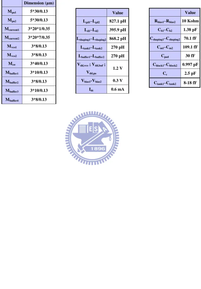
Table 2-1 Summary of device value 42
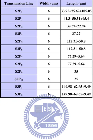
Table 2-2 Dimension summary of transmission line 43
Table 2-3 Summaries of original post-sim results1 53
Table 2-4 Summaries of original post-sim results2 53
Table 3-1 Summaries of measurement results 61
Table 3-2 Summaries of revised post-sim results 68
Table 3-3 Dimensions summaries of the re-design version 70 Table 3-4 Comparison with other K-band power amplifiers 74 Table 3-5 Comparison with other K-band power amplifiers 74
Table 3-6 Summaries of re-design post-sim results 75
Figure Captions
Fig. 1-1 24-GHz service band plan release by FCC 1
Fig. 1-2 Class E power amplifier 3
Fig. 1-3 Drain voltage and current waveforms of ideal class E power amplifier
3
Fig. 1-4 Schematic of proposed class E power amplifier in [9] 5 Fig. 1-5 Schematic of proposed current-mode power amplifier in [10] 5 Fig. 1-6 Schematic of proposed K-band power amplifier in [11] 6 Fig. 1-7 Schematic of proposed 24 GHz power amplifier in [12] 8 Fig. 1-8 Schematic of proposed 24 GHz power amplifier in [13] 9
Fig. 2-1 Block diagrams of polar loop structure 15
Fig. 2-2 The load network of class E power amplifier 17 Fig. 2-3 Voltage and current waveforms of class E power amplifier 17 Fig. 2-4 Response of class E power amplifier when the transistor turns off 18 Fig. 2-5 Effect for optimal load when swing is limited 19 Fig. 2-6 Optimal load resistance determined by load-line analysis 20 Fig. 2-7 Neutralization for resonating parasitic Cgd 22 Fig. 2-8 Small-signal model of common-source transistor 22 Fig. 2-9 Equivalent network between gate-drain of common-source
transistor
25
Fig. 2-10 Equivalent network between gate-drain of common-source transistor (L’gd is the combination of Lgd and Cb)
25
Fig. 2-11 The load network of ideal case class E power amplifier 26 Fig. 2-12 The load network of Ron case class E power amplifier 28
Fig. 2-13 Schematic of designed power amplifier 31
Fig. 2-14 Stability factor (k factor) 33
Fig. 2-15 Stability means (b factor) 33
Fig. 2-16 Constant Pout, constant PAE contours and the chosen ZL 35 Fig. 2-17 Impedance transformation network of power amplifier 35 Fig. 2-18 Load impedance transferred by transformation network 36
Fig. 2-20 The design of voltage-controlled oscillator with cascode buffer 39
Fig. 2-21 Schematic of designed whole circuits 41
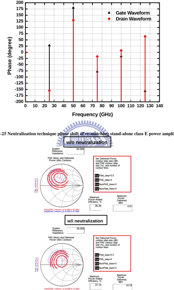
Fig. 2-22 Schematic of designed whole circuits (with parasitic routing effect) 41 Fig. 2-23 Layout, 3-D model and setting for EM analysis (2-port networks) 41 Fig. 2-24 With and without neutralization technique analysis of re-matching
stand-alone class E power amplifier
45
Fig. 2-25 Neutralization technique phase shift of re-matching stand-alone class E power amplifier
46
Fig. 2-26 Neutralization technique phase shift effect 46 Fig. 2-27 Drain voltage and current waveforms with gate voltage waveform
of re-matching stand-alone class E power amplifier
47
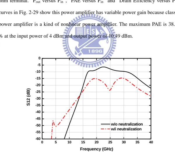
Fig. 2-28 Large signal S-parameter (LSSP) for re-matching stand-alone class E power amplifier
47
Fig. 2-29 Pout vs Pin, PAE vs Pin and Drain Efficiency vs Pin for re-matching stand-alone class E power amplifier
48
Fig. 2-30 Tuning range of voltage-controlled oscillator 49 Fig. 2-31 Phase noise of voltage-controlled oscillator 49
Fig. 2-32 Pout vs Vtune for whole circuits 50
Fig. 2-33 Overall drain Efficiency vs Vtune for whole circuits 51 Fig. 2-34 Output power spectrum for whole circuits 51 Fig. 2-35 Pout vs Pin, PAE vs Pin and Drain Efficiency vs Pin for cascode
buffer with power amplifier
52
Fig. 3-1 Chip microphotograph of the proposed whole circuits 55 Fig. 3-2 Measurement setup for the proposed whole circuits 56 Fig. 3-3 Measured output frequency v.s. tuning voltage for proposed whole
circuits
58
Fig. 3-4 Measured output power v.s. tuning voltage for proposed whole circuits
58
Fig. 3-5 Measured phase noise for proposed whole circuits 59 Fig. 3-6 Measured output power spectrum for proposed whole circuits 59 Fig. 3-7 Pout vs Pin for cascode buffer with power amplifier 60
amplifier
Fig. 3-9 The crossover MOS line and the effect in the gate waveforms of Mbuffer4
63
Fig. 3-10 Layout view and 3-D model in HFSS for revised post-simulation 64 Fig. 3-11 Output frequency of revised post-sim comparing with original
post-sim and measurement
65
Fig. 3-12 Output power of revised post-sim comparing with original post-sim and measurement
65
Fig. 3-13 Phase noise of revised post-sim comparing with original post-sim 66 Fig. 3-14 Pout vs Pin of revised post-sim comparing with original post-sim
and measurement
66
Fig. 3-15 PAE and drain efficiency vs Pin of revised post-sim comparing with original post-sim and measurement
67
Fig. 3-16 Change components’ dimensions for re-design 70 Fig. 3-17 The modified layout for re-design whole circuits 71 Fig. 3-18 Output frequency of re-design comparing with original and
revised post-sim
71
Fig. 3-19 Output power of re-design comparing with original and revised post-sim
72
Fig. 3-20 Phase noise of re-design comparing with original and revised post-sim
72
Fig. 3-21 Pout vs Pin of re-design comparing with original and revised post-sim
73
Fig. 3-22 PAE and drain efficiency vs Pin of re-design comparing with original and revised post-sim
Chapter 1
Introduction
1.1.
Background
Recently, the research on radio-frequency integrated circuits (RFICs) in higher frequencies have been accelerated since the frequency spectra below 10 GHz have gradually become crowded by massive requirements of data transmission from the modern wireless applications such as Bluetooth, wireless local area network (WLAN) and ultra-wideband (UWB), etc. Many researchers investigate RF transceiver front-end circuits in 24 GHz because higher operating frequency can provide more bandwidth. In addition, the 24.05–24.25-GHz Industrial, Scientific, and Medical (ISM) band [1], 22–29 GHz band provided by Federal Communications Commission (FCC) for the operation of vehicular radar [2]–[3], and the 24-GHz band plan as shown in Fig. 1-1 [4] are released.
In RF transmitter front-end, key components such as voltage-controlled oscillators (VCOs) and power amplifiers (PAs) have been reported in many CMOS designs [5]–[7]. Nevertheless, in standard CMOS technologies, the active devices have poor inherent characteristics comparing to GaAs and SiGe, and the passive components such as planar inductors have higher losses from lossy substrate. These inherent characteristics seriously degrade the performance of the transmitter front-end circuits. However, today’s consumers demand wireless systems that are low-cost, power efficient, reliable and have a high integration form. High levels of integration are desired to reduce cost and achieve compact form. Hence the long term vision of goal for wireless transceiver is to merge as many components as possible to a single die in an inexpensive technology. Therefore, there is a growing interest in utilizing CMOS technologies for RF power amplifier (PAs) [8]. Although the output power of the transmitter can be increased by utilizing multiple parallel transistors to implement power amplifiers [5], the power-added efficiency (PAE) remains the same in such a structure. To improve the PAE, several design techniques have been proposed. By using the special structure of transmission line and additional algorithms, the PAE of a RF CMOS PA can be improved to around 10% [6]–[7].
1.1.1. Review on Class E Power Amplifier
Class E power amplifier is a single transistor operated as a switch. It uses a high order reactive network to shape the switch voltage to have both zero value (zero voltage switching; ZVS) and slope (zero derivative switching; ZDS) at the switch turn-on. Therefore, the ideal efficiency is 100 %. A class E power amplifier is showed inFig. 1-2. The drain voltage and current waveform of ideal class E power amplifier is showed inFig. 1-3.
V
in
M
pa
V
dd,pa
RFC
C
shunt
R
L
L
shaping
C
shaping
V
out
V
c
I
d
Fig. 1-2 Class E power amplifier
Obviously, the current of the transistor is near maximum when the switch turns off. However, it will introduce a significant switch turn off losses because the switch is not infinitely fast. Hence, it will reduce the efficiency. Another drawback is the large peak voltage approximately 3.56 Vdd,pa when the switch sustains in the off state.
Therefore, it needs a high breakdown voltage and is not a good choice for short-channel devices.
An 18 GHz fully-integrated class E power amplifier is proposed in [9], as shown in Fig. 1-4. It consists of a two-stage cascode amplifier, a common source driver, and an output stage. Due to the limited voltage headroom, common-source amplifiers are used in the last two stages. The cascode amplifiers are used to provide sufficient gain, good input matching and isolation from the last two stages which potentially could oscillate. Besides, this proposed fully-integrated class E power amplifier also adopts a mode-locking (also known as injection-locking) technique exploiting the instability of driver amplifier which is used to improve the drive for the gate of output stage. The mode-locking technique actually increases the gain of the circuit and reduces the drive requirement for switching the output transistor. The comparison table in [9] shows that this class E power amplifier has significantly higher efficiency and lower input requirement than that for the previously reported CMOS PA operating near 20 GHz. It also suggests CMOS technology is a viable candidate for building fully-integrated transmitter near 20 GHz. But the method of its isolation is too complicated; we develop another kind of isolation technique to improve this disadvantage as will be discussed after. Due to the limited voltage headroom, the power supply of [9] is too high and the power added efficiency (PAE) is not high enough.
Fig. 1-4 Schematic of proposed class E power amplifier in [9]
1.1.2. Review on K-Band (18 - 26.5 GHz) Power Amplifier
Schematic shown in Fig. 1-5 is a 24 GHz current-mode power amplifier proposed in [10]. It is accomplished by using two-stage cascade current-mirror structure and it also operates in class AB mode. Besides, the proposed current-mode power amplifier also uses L7 and L8 to resonate the device capacitance between gate and drain of M8
and M10. It also uses R3 for low frequency stability consideration. And the optimized
output impedance transfer network is determined by the load-pull simulation. From the comparison table in [10], it shows that the proposed CMOS current-mode power amplifier has the highest PAE and the largest output power among the RF PAs.
Fig. 1-5 Schematic of proposed current-mode power amplifier in [10]
Schematic shown in Fig. 1-6is another K-band power amplifier proposed in [11]. It is composed of 3 stages. The first two stages are driver stage, and the third stage is
formed by two parallel power cells. The typical topologies of the CMOS transistors are common source and cascode. The biasing point of this design is at class A for better linearity. The devices selected in the power cell were determined by the load-pull simulation from the large signal model provided by TSMC, and the Gmax simulation.
The power stage includes two power cells. And the power cells are in-phase combined directly. Two odd-mode suppression resistors of 11 Ω are placed within two power
cells for stability consideration. Each power cell was pre-matched to 100 Ω by an appropriate matching network before binary combining. The matching network includes an inductor (used for inductive peaking), and impedance transform network, which is implemented by thin film micro-strip lines (TFMS) used for lower loss than lumped elements for wide band power match. Appropriate bypass circuits are placed at each bias point for low frequency stability consideration. The comparison table in [11] shows that the proposed K-band power amplifier has the highest gain and good output power in standard CMOS process.
Schematic shown in Fig. 1-7 is a 24 GHz power amplifier proposed in [12]. By shunt combining N times transistors with device size of (W/N), the parasitic capacitance Cgd of each transistor is reduced, which means higher gain and output
power performance are maintained. The binary combining method is a simple way to combine output power of each transistor with equal phase and loss. To maintain low loss in output matching circuits with good stability at low frequency, output high pass matching network is chosen. A shunt short stub is connected to the device to resonance the parasitic capacitance and provides dc biasing path. By shunting the resonance stubs, the optimum load impedance is calculated via the load line estimation and the load-pull simulation. The T-shaped high-pass matching is used as impedance transformer and ensures the low frequency stability. In order to achieve higher gain and better linearity performance, the cascode pairs are all biased in class A. It also uses thin-film micro-strip line (TFMS) for interconnection and matching stubs. The proposed 24 GHz power amplifier provides larger gain and power compared to commercial designs. From the comparison table in [12], the proposed power amplifier shows the highest OP1dB and saturation power among the CMOS PAs above 20 GHz.
VDD VDD 32 fingers 160 m width Binary combination T-matching Ropt 25 Ω RFin 50 ohm RFout 50 ohm Thin Film Micro-Strip Line
(TFMS)
Fig. 1-7 Schematic of proposed 24 GHz power amplifier in [12]
Schematic shown in Fig. 1-8 is a 24 GHz power amplifier proposed in [13]. The PA has two gain stages with each gain stage consisting of a cascode transistor pair to ensure stability and increase breakdown voltage. The PA is designed to operate in class AB mode. The output and inter-stage matching networks in the PA are realized with the substrate-shielded coplanar waveguide structure to reduce power losses and area. The substrate-shielded coplanar waveguide is leading to more than a factor of two reductions in wavelength at 24 GHz when compared to a standard coplanar waveguide structure in silicon dioxide. The short wavelengths can improve isolation and make this structure particularly suitable for integrating multiple power amplifiers on the same die. Amplifier stability is improved by the RC network at the input of each stage, which guarantees low frequency stability.
1.2.
Motivation
This research focuses on the novel approach for designing and implementing 24-GHz transmitter circuits by CMOS technology.
Because of the applications released in 24-GHz frequency range, many researchers are attracted to design high-performance and low-cost wireless applications in this frequency band with advanced CMOS technologies. However, CMOS technology has limitation of low supply voltage. That is why traditional commercial implementation of wireless transceivers typically utilizes a mixture of technologies in order to implement a high-performance, completed system. Nevertheless, considering the cost and integration capability, CMOS technology is still the most suitable choice for designing RF circuits.
When implementing 24-GHz transmitter circuits by CMOS technology, the output power of the transmitter can be increased by utilizing some structures to implement power amplifiers. The higher output power can be achieved, but the power-added efficiency remains the same in such structures. Therefore, the improvement of the PAE of a RF CMOS PA at the higher output power level is a main course of discussion. According to theses reasons as mentioned above, the class E power amplifier compared with other class of power amplifiers at K-band as the Table 1-1 shown can provide higher power-added efficiency. Therefore, at 24-GHz, we adopt the class E power amplifier as our design which tries to improve the PAE of a RF CMOS PA at the higher output power level and use the voltage-controlled oscillator as the input signal of class E power amplifier. The use of class E power amplifier has solved the design conflict between improvement of power efficiency and maintenance of amplifier linearity in K-band system. Besides, in order to solve the isolation problem, a neutralization technique must be developed.
[9] *[10] [11] [12] [13] Technology 0.13-µm CMOS 0.13-µm CMOS 0.18-µm CMOS 0.18-µm CMOS 0.18-µm CMOS
Topology Class E Class AB Class A Class A Class AB
Supply Voltage (V) 1.5 1.2 3.6 3.6 2.5 Freq (GHz) 18 20 24 18-23 24 24 Output Power (dBm) 10.9 10.2 17.1 20.1 22 14 Peak PAE (%) 23.5 20.5 23.9 9.3 20 6.5 Chip Area (mm2) 0.782 1.05 2.4 0.42 14.28
*[10] : redesign post-sim results of proposed power amplifier in [10]
1.3
. Main Results and Thesis Organization
In this work, the voltage-controlled oscillator and class E power amplifier are designed. The voltage-controlled oscillator is realized by cross-coupled NMOS with LC tank and PMOS current source oscillator. Besides, the voltage-controlled oscillator cascades with a cascode buffer. A differential single stage common source class E amplifier is proposed for the power amplifier. This is the first work including a voltage-controlled oscillator and a power amplifier for K-band applications.
Measurement results show that the measured output center frequency and maximum output power are 23.2 GHz and –2.41 dBm, respectively. The measured phase noise is -108 dBc at 10 MHz. The measured output power of cascode buffer with power amplifier is lower than original post layout simulation about 13 dB. And the measured total power consumption of VCO and power amplifier is 29.4 mW from 1.2 V power supply. From the analysis, experimental results, and re-design circuit, the proposed circuit is suitable for high efficiency application.
The post layout simulation results of the re-design circuits show that the output center frequency and maximum output power are 24.26 GHz and 10.41 dBm, respectively. The phase noise is -119.9 dBc at 10 MHz. The output power of cascode buffer with power amplifier is almost the same to the original post layout simulation. And the total power consumption of VCO and power amplifier is 56.13 mW from 1.2 V power supply. The power consumption is less than other type power amplifier because the class E power amplifier operates at the threshold voltage.
The thesis is divided into five chapters. Chapter 1 introduces the background, motivation and main results of this research. The whole circuit design and simulation results of this thesis will be presented at Chapter 2. Design considerations are discussed in Section 2.1. Then the power amplifier, voltage-controlled oscillator and
the whole circuits design procedures are presented in Section 2.2.1, 2.2.2, and 2.2.3, respectively. Post-simulation results are shown in Section 2.3.
The chip microphotograph, measurement setup, experimental results, revised post simulation and re-design will be included in Chapter 3. Finally, the conclusions and future work will be presented in Chapter 4.
Chapter 2
Circuit Design and Simulation Results
2.1.
Design Considerations
How to use CMOS technology to design large-signal transmitter front-end circuits is the most challenge part. In order to obtain enough trans-conductance, the transistors’ sizes must be increased. However, the larger the size it is, the more serious parasitic effect it will be. The parasitic capacitance effect will provide leakage path for high-frequency signal or degrade reverse isolation and stability. In this research, these leakage paths for RF signal and stability-degraded effects are resonated and neutralized by on-chip inductors, respectively. The output matching network of power amplifier is determined by load-pull analysis which considers the imaginary part caused by the parasitic effect.
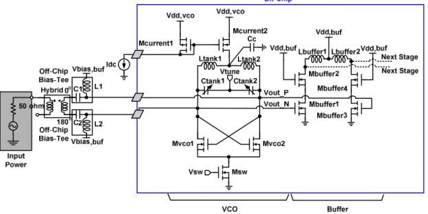
The block diagrams ofpolar loop structure are shown in Fig. 2-1.In this research, as shown in Fig. 2-1, the proposed circuits included a voltage-controlled oscillator with cascode buffer and a class E power amplifier are realized with 0.13-µm standard CMOS technology. The designed VCO is implemented by the cross-coupled NMOS with LC tank concept in order to provide a signal source for class E power amplifier. The class E power amplifier is also realized by push-pull concept. The 1st-stage of cascode buffer the RF signal comes from designed VCO to drive the 2nd-stage of class E power amplifier. The 2nd-Stage is designed to have capability to provide enough signal swing that the required output power can be achieved. The specification of the designed whole circuits is to output more than 10-dBm output power at 24 GHz.
L im it e r L O 2 _ Q L O 2 _ I
2.2.
Circuit Design
2.2.1. Class E Power Amplifier
Class E power amplifiers (PA) have been proved to be popular radio frequency (RF) PAs with high efficiency. Using Class E power amplifier can maintain high enough efficiency at high output power level. To achieve high enough efficiency, the output load network must be carefully designed to eliminate the overlap between voltage and current waveform at the designated operating frequency and output power level. Generally speaking, the transistor output capacitance included the parasitic capacitances constructs an optimum parallel reactance at the output load network and satisfies the optimum Class E power amplifier conditions. The conditions of Class E power amplifier were given by Sokal [14], and can be put in the form:
( ) 0 E (2.1) 0 on sw on sw t v t Class dv dt = ⇔ =
Where ton represents the instant at which the switch closes, and vsw(t) represents the
switch voltage. These conditions can be guaranteed by the use of the load network shown inFig. 2-2. And the voltage and current waveforms of Class E power amplifier are also shown in Fig. 2-3. Above equations show the typical properties of Class E power amplifiers, where the passive components are used to minimize the drain-source voltage when the switch closes. This property of Class E power amplifiers is usually called “zero voltage switching”. Furthermore, another one property can demand that the derivative of the switch voltage also equals zero at the switching moment. Which is usually called “zero derivative switching”. These demands will make the amplifier less sensitive to timing errors and component variations [15].
After the switch turns off, the load network operates as a damped second-order system as shown in Fig. 2-4 with initial conditions across Cp and Cs and in Ls. The
time response depends on the quality factor Q of the network for underdamped, overdamped, and critically damped conditions. We note that in the last case, VX
approaches zero volt with zero slope.
Fig. 2-4 Response of class E power amplifier when the transistor turns off
When implementing a power amplifier at high output power level, the most critical node in the power amplifier circuit is its output node and resultant large voltage and current swing are required. Operated at high output power level which implies to need large DC bias means that the reliability such as metal current density must be considered. Besides, large voltage and current swing which implies to the large-signal operation viewpoint must also be considered with the small-signal operation viewpoint at the same time. Therefore, for the power amplifiers of RF systems, the output impedance transformation networks (output matching networks) are always implemented by load-line or load-pull analysis method instead of traditional conjugate matching analysis method.
The traditional conjugate matching analysis method can provide maximal power transfer only under the condition of no current and voltage swing limitation. In other words, it is always true for small-signal operation. That’s why most of RF systems, such as receiver, adopt traditional conjugate matching analysis method for their matching networks. However, in the transmitter front-end, especially for the output of power amplifier, the large voltage and current swing are large signal operation
viewpoints. Because the output of power amplifier always produces high output power level, the current or voltage swing always reaches the limitation of its supply. Therefore, the output matching networks of power amplifiers are usually determined by two methods – load-line or load-pull analysis methods instead of traditional conjugate matching analysis method.
Fig. 2-5shows the quantitative description of the above analysis methods for the difference of optimal load if the voltage and current swing are limited. For traditional conjugate matching analysis method, the load resistance RLOAD is chosen to equal to
RS. Under the voltage and current swing are limited conditions, the “VMAX/IMAX” load
resistance has maximal output power delivered capability than any other load resistance.
Fig. 2-5 Effect for optimal load when swing is limited
The hand-calculated procedure for load-line analysis can be accessed through (2.2)–(2.3). , = ( DC- knee) DC (2.2) OUT MAX 1 P V V I 2 , -= DC knee (2.3) L OPT DC V V R I
According to these equations, the load-line analysis on a common-source transistor I-V curve is illustrated in Fig. 2-6.
R
L>R
L,OPT(lower current swing)
V
kneeV
DCV
MAXV
DSI
DI
MAXI
DCR
L=R
L,OPTR
L<R
L,OPT(lower voltage swing)
Fig. 2-6 Optimal load resistance determined by load-line analysis
The black color load-line is the optimal load resistance determined by load-line analysis. And the optimal load resistance value also equals “VMAX/IMAX”. It shows that
the black color load-line has maximal output power under this voltage and current swing limitation. The red color load-line is the load resistance which is smaller than the optimal resistance. It will have the same current swing but smaller voltage swing and resultant smaller output power. The blue color load-line is the load resistance which is larger than the optimal resistance. It will have the same voltage swing but smaller current swing and resultant smaller output power.
Based on the figures and equations of load-line analysis above, the load-line analysis can be used for quickly determining optimal load resistance, but not reactance. That is, only the real part of the load impedance (ZL) can be determined by
this analysis, the effect of imaginary part caused by the parasitic effect of the circuit will be completely neglected. Because the load-line analysis bases on I-V curve, the junction parasitic effect is exclusive. Unfortunately, when the signal is operated at high frequency, the parasitic effect induces lose. Besides, the larger size of the transistor it is, the parasitic effect is worse and cannot be ignored.
Considering the parasitic effect and comparing to the load-line analysis, the load-pull analysis can be used to determine the load impedance ZL, both real and
imaginary part, of power amplifiers. The load-pull analysis is mainly to sweep ZL to
see how PAs perform. The analysis procedures are:First, add a load tuner (ZL) at the
output of power amplifier. Second, sweep the value of load tuner (ZL) to see the
difference of output power (POUT) and power-added efficiency (PAE). Because of each
point on Smith chart is a reflection coefficient, and the reflection coefficient and impedance are one-to-one mapping for 50 Ω characteristic impedance. When changing the value of load tuner (ZL), the swept data of the same output power and
the same PAE was recorded. The swept data can be used to construct constant POUT
and constant PAE contours. Third, choose one reflection coefficient (load impedance) on Smith chart by trade-off between constant POUT and constant PAE contours. Using
load-pull analysis to determine ZL has several advantages. Because the constant POUT
and PAE contours are drawn on the same Smith chart, it is easy and obvious to trade-off between them. Besides, because of the one-to-one mapping characteristic, both real and imaginary part of ZL can be determined as soon as the trade-off point
has been chosen.
Another difficulty for designing power amplifier is the parasitic effect. Because high output power is required, a large size of each transistor and resultant seriously parasitic effect are inevitable. Large parasitic Cgd provides a short path between input
and output at high frequency in common-source amplifier. Therefore, a resonated inductor (Lgd) must be added between these two nodes shown in Fig. 2-7 for
Fig. 2-7 Neutralization for resonating parasitic Cgd
The small-signal model for a common-source amplifier is shown in Fig. 2-8. Because the S-parameter S12 is desired, input phasor E2 is placed at port 2 (drain).
Fig. 2-8 Small-signal model of common-source transistor
According to the definition of S12 shown in (2.4)[16], the term “VO1/E2” can be
expressed by (2.5). Although equations (2.4) and (2.5) can show the effect for value of ZX, it is not obvious. In order to further simplify this equation, the matched condition
at output node is assumed. This condition is always true for RF systems. The S22 of common-source amplifier can be calculated through (2.6) to (2.7). α and β are the substituted variables for the numerator and denominator in (2.6), respectively. Under the matched condition, the condition “ZO2β=α” can be derived as shown in (2.8). Thus
the equation (2.5) can be further simplified by this derived condition and the final result for S12 of common-source amplifier is shown in (2.9).
For a traditional common-source amplifier, ZX is “1/jωCgd” and S12 will become
Cgd it has and worse the reverse isolation it becomes. For extremely case of infinitely
large Cgd value, the S12 will become the equation shown in (2.11) and equal to 1 (or 0
dB) in general for RF circuits (for ZO1 = ZO2 = ZO = 50 ohm, general case in RF
circuits). 0-dB S12 means this circuit has no any reverse isolation or the equivalent circuit for this two-port network is short circuit. It is reasonable because the infinitely large Cgd provides a zero-impedance short path between port-1 and port-2.
If the resonated inductor Lgd is adopted and placed between gate-drain, the
impedance ZX in (2.9) will become (2.12). Thus S12 can be zero as long as the
condition in (2.13)is achieved. That is the reason why a resonated inductor is always adopted for large-sized common-source amplifier.
O 2 O 1 2 O 1 Z V S12 2 E Z ≡ × × ≡ × × ≡ × × ≡ × × (2.4) (((( )))) (((( )))) (((( )))) (((( )))) O 1 O 1 GS DS 2 O 2 m O 1 GS DS X O 1 X GS O 1 GS O 1 DS GS DS DS X O 1 X GS O 1 GS V Z Z Z E ====Z ×××× g Z Z Z ++++ Z Z ++++Z Z ++++Z Z ++++ Z Z ++++Z Z ++++Z ×××× Z Z ++++Z Z ++++Z Z (2.5)
((((
))))
((((
)))) ((((
DS X O 1 X GS O 1)))) ((((
GS))))
T 2 m O 1 GS DS X O 1 X GS O 1 GS O 1 DS GS DS Z Z Z Z Z Z Z Z g Z Z Z Z Z Z Z Z Z Z Z Z Z × + + × + + × + + × + + ==== + + + + + ++ ++ ++ ++ ++ + + + + + (2.6) T 2 O 2 O 2 T 2 O 2 O 2 Z - Z α- Z β S 22 Z Z α Z β ≡ = ≡ = ≡ = ≡ = + + + + + + + + (2.7) O 2 S22→→→→0⇒⇒⇒⇒Z β====α (2.8) O 2 O 1 O 2 O 1 GS DS 2 O 2 O 1 O 1 Z V Z Z Z Z S12 2 2 E Z β α Z Z ≡ × × = × × ≡ × × = × × ≡ × × = × × ≡ × × = × × ++++ ((((
))))
O 2 O 1 GS DS X O 1 DS GS DS O 1 GS DS O 1 Z Z Z Z Z Z Z Z Z Z Z Z Z = × = × = × = × + + + + + + + + (2.9)((((
))))
O 2 O 1 GS DS O 1 O 1 DS GS DS O 1 GS DS gd Z Z Z Z S12 Z 1 Z Z Z Z Z Z Z jωC = × = × = × = × ×××× ++++ ++++ (2.10) O 2 O 1 Z S12 Z ≈≈≈≈ (2.11) gd X gd 2 gd gd gd jωL 1 Z jωL // jωC 1 ω L C = = = = = = = = −−−− (2.12) 2 gd gd X if ω L C ====1⇒⇒⇒⇒Z → ∞→ ∞→ ∞→ ∞⇒⇒⇒⇒S12→→→→0 (2.13)For RF system, an ideal inductor is equal to a short path for DC because its impedance is “jωL”. Therefore, as long as the resonated inductor is implemented, a blocking capacitor is always used for blocking unnecessary DC path. This blocking capacitor, Cb, comes from the consideration during measurement. The cable inherent
resistance between probe and DC power supply is around 3 Ω. It’s not a serious issue for small-signal systems such as receiver front-end. However, for hundreds milli-ampere transmitter front-end, it may cause milli-volt or even several volts drop during measurement. Because such voltage drop may downgrade internal biasing points by different levels, DC current may be sunk into unexpected path when measurement. In order to avoid this phenomenon, a capacitor must be added to block DC current from stage to stage.
Fig. 2-9 is the equivalent network between gate-drain of common-source transistor. If Cb is an ideal blocking capacitor (infinite large), parasitic Cgd can be
resonated by Lgd at desired frequency to increase reverse isolation. However, the
effective value of inductor (L’gd in Fig. 2-10) is slightly smaller than Lgd. It will
slightly shift the resonant frequency caused by L’gd and parasitic Cgd. This problem
can be corrected by fine tuning the value of Lgd [10].
Fig. 2-9 Equivalent network between gate-drain of common-source transistor
Fig. 2-10 Equivalent network between gate-drain of common-source transistor (L’gd is the combination of Lgd and Cb)
By (2.2)–(2.3), the transistors’ dimensions and optimal load resistance can be roughly predicted by hand calculation. Because the biasing is fixed to VDD, the variable for
transistor itself is size. And the operation mode is class E, the gate biasing is also fixed to the transistor threshold voltage. The transistor’s size is also determined by the required output power. In order to determine the transistor’s size, some analysis steps
operates at ideal case which means that the transistor turn-on resistance ideally equals zero. According to the assumption, some initial design steps can be provided. But because of the assumption, these initial design steps are not suited to design the circuits. These initial design steps can only determine some initial circuit parameters. Therefore, the transistor turn-on resistance should be considered and the modified design steps could be provided. These design steps are shown below. The load network of ideal case class E power amplifier is shown in Fig. 2-11.
Fig. 2-11 The load network of ideal case class E power amplifier
At first, the output node Vo is described in (2.14). And we get Io in (2.15). The voltage of the shunt capacitor Vc can be calculated through (2.16) to (2.18). In order to get c1, we use the Fourier integral as shown in (2.19) and (2.20). Equation (2.21)
and (2.22) show the results of the Fourier integral. Because RF choke has no voltage drop, the average voltage of Vc is Vcc. Therefore we can get equation (2.23). By the equation (2.23), we can define the equal load resistance RDC measured from the power
supply. According to this, the output AC power can be shown in (2.24). The overall drain efficiency η also can be shown in (2.25). The amplitude A of output waveform equals a constant c. ( ) sin( ) sin( ) (2.14) Vo
θ
=cω ϕ
t+ =cθ ϕ
+ : ( ) ( ) sin( ) (2.15) : L Lc output voltage magnitude
Vo c
io where
phase difference at output
R R
θ
θ
θ ϕ
ϕ
= = + 1 ( ) ( ) (2.16) 0 c V Ic u du Bθ
θ
= ∫ ( ) ( ) sin( ) (2.17) c t t L c I u I Io u I u R ϕ = − = − +( ) t [cos( ) cos ], B (2.18) c shunt L I c V c B BR θ θ θ ϕ ϕ ω ∴ = + + − ≜ 2 1 1 0 2 1 0 1 ( ) sin( ) (2.19) 1 0 ( ) cos( ) (2.20) c c c V d V d π π
θ
θ ϕ θ
π
θ
θ ϕ θ
π
= + ∫ = ∫ + 1 1 1 1 cos 2 sin ( , , , , ) (2.21)sin 2 cos cos 2 t L t L L L c I R I R h B R P where c c BR
π
ϕ
ϕ
ϕ ψ
ρ
π
π
ρ
ψ
ϕ
ϕ
− = ⋅ ⋅ ⋅ ⋅ = − + ≜ 1 1 1 1 sin 2 cos ( , ) = (2.22)2 cos sin cos
2 t L t L c I R
π
ϕ
ϕ
I R gϕ ψ
whereψ ϕ ϕ
π
ϕ
ϕ
ψ
+ = ⋅ ⋅ ⋅ ⋅ − + ≜ 2 2 0 1 1 ( ) [ 2 sin cos ] (2.23) 2 2 2 cc c t t DC V V d I g g I R B ππ
θ θ
ϕ π
ϕ
π
π
=∫
= ⋅ − − ≜ ⋅ 2 2 2 2 2 2 t 2 ( ) 1 1 2 = I (2.24) 2 2 2 cc L out L L L DC c V g R c P g R R = R ⋅ = R ≜ 2 (2.25) 2 out L DC DC P g R P Rη
≜ = ⋅According to the class E power amplifier boundary equation, we can get equation (2.26) and (2.27). We can get (2.28) from (2.26) and (2.29) from (2.27). So the φ equals -32.4820 or -0.5669 rad. Because the ideal drain efficiency of class E power amplifier η is 100 %, we can get a group of initial design values through (2.30) to (2.36). ( ) 0 (2.26) ( ) 0 (2.27) c c V dV d θ π θ π
θ
θ
θ
= = = = cos (2.28) 2gπ
ϕ
= 1 sin (2.29) gϕ
=− 0 =-32.482 =-0.5669 rad (2.30)ϕ
L 1 =1.7337R (2.31) DC R B π = 1 (2.32) 5.4466 L B R = 0 =49.052 =0.85613 rad (2.33)
ψ
L X=1.1525R (2.34) c max V ( )θ
=3.562V (2.35)cc cc c=1.074V (2.36) Next, the transistor turn-on resistance should be considered and the modified design steps could be provided. These design steps are also shown below. The load network of Ron case class E power amplifier is shown in Fig. 2-12.Fig. 2-12 The load network of Ron case class E power amplifier
At first, the output node Vo also can be described in (2.37). Therefore we get Io in (2.38). So the node V1 can be described in (2.39). Because the transistor has the on state and off state, the voltage of the shunt capacitor Vc can be calculated in two equations (2.40) and (2.41). According to the two boundary equations (2.42) and (2.43), we can get (2.44). The amplitude A of output waveform equals a constant c.
( ) sin( ) (2.37) o V θ ≜c θ ϕ+ ( ) ( ) o sin( ) (2.38) o L L V c i R R θ θ = = θ ϕ+
1 1 1 2 1 1 2 2 1 1
( ) sin( ) sin( ) sin( )
1 ( ) tan , 1 ( ) 1 tan (2.39) tan L L L L L c V c jX c R X c c c R X X where R R X R
θ
θ ϕ
θ ϕ
θ ϕ
ρ
ϕ
ϕ
ρ
ψ
ψ
− − = + + + = + = ⋅ + = + = + = + ≜ ≜ , [ sin( )] (2.40) c on t on L c V I R R θ ϕ = − + × , 0 0 1 1( ) = [ sin(u + )] = t [cos( ) cos ] (2.41)
c off c t L L I c c V I u du I - du B B R B BR θ θ
ϕ
θ
θ ϕ
ϕ
=∫
∫
+ ⋅ + − , ( 0) , ( 2 ) (2.42) c off c on V θ = =V θ = π , ( ) , ( ) 0 (2.43) c off c on V θ π= =V θ π= = [ sin( )] , 2 ( ) (2.44)[cos( ) cos ] [ sin ], 0
t on L c t on t L L c I R R V I c c R I B BR R
θ ϕ
π θ
π
θ
θ
θ ϕ
ϕ
ϕ
θ π
− + × ≤ ≤ = + ⋅ + − + − ≤ ≤ Next, we also use the Fourier integral to get c1 which is described through (2.45)
to (2.48). For high efficiency of class E power amplifier, Vc(θ=π) equals zero at the
instant that the transistor turns on as shown in (2.49). Therefore we can get equations (2.50) and (2.51). For high efficiency of class E power amplifier, dVc(θ)/dθ at
θ=π equals zero. As a result, we can get equation (2.52). And the average voltage of Vc(θ) equals Vcc’, equation (2.53) can be obtained. According to (2.53), we can define
the dc resistance RDC in (2.54). Through (2.50) to (2.52), the dc resistance RDC can be
derived in (2.55).
1 1
1 1
cos 2 sin
(2.45)
sin 2 cos cos 2 sin cos cos
2 2 t eq L on on c I R BR BR BR