DOI 10.1007/s00542-014-2211-y TechnIcal PaPer
A battery charge controller realized by a flyback converter
with digital primary side regulation for mobile phones
Paul C.‑P. Chao · Wei‑Dar Chen · Ruo‑Hua Wu
received: 30 October 2013 / accepted: 28 april 2014 / Published online: 18 May 2014 © Springer-Verlag Berlin heidelberg 2014
1 Introduction
While the market of electronic products such as mobile phones and portable devices grows rapidly, the demand of lithium battery for fast charge, long duration, and long life cycle increases significantly as well (hwang et al. 2007; Do Valle et al. 2011). as aiming the best performance out of a battery, the controller for a battery charging system plays an important role to command the battery. There are several available charge methods for a lithium battery, such as con-stant current (cc)/concon-stant voltage (cV) charge (Fakham et al. 2011; linden and reddy 2001), pulse charge (Paul et al. 2013) and reflex charge (chen et al. 2008), etc. To render the best charging performance for a lithium battery, a single-stage flyback converter designed with functions of battery cc/cV charging is proposed in this study. In gen-eral, a flyback converter has been widely used for Dc–Dc conversion due to its low-cost, wide power range, and gal-vanic isolation between input and output stage. The con-ventional flyback converter often contains an opto-coupler and an operational amplifier in the feedback loop (chen et al. 1999; Kleebchampee and Bunlaksananusorn 2005). The opto-coupler is sensitive to temperature variation that will be a limit temperature in operating. The opto-coupler and operational amplifier also make the system compli-cated and extra cost. To solve these problems, this study adopts primary side regulation (PSr) technique to sense the output voltage.
The battery charge controller with flyback converter has been developed in digital control with opto-coupler feed-back (hua and hsu 2005; li and Zheng 2010; chen and lai 2012). The conventional flyback converter with cc or cV applications always requires two sensed aDc channels as feedbacks for regulating (Thang et al. 2013; lin et al. 2012; hsieh and huang 2011). an improved duty control Abstract a flyback converter with digital control
designed and implemented for a lithium battery charg-ing system is proposed in this study. as opposed to the requirement of both voltage and current feedbacks for a conventional flyback converter, this study proposes a con-verter structure that needs only one voltage feedback to stabilize converter output for implementing the designed battery charging techniques. This single feedback of volt-age is made possible by so-called “primary side regula-tion (PSr)”, which in hardware senses the output voltage using an auxiliary winding in the isolating transformer of the flyback converter that is operated in Dc–Dc discon-tinuous current mode. The adoption of PSr also enables the elimination of the opto-coupler that is often used in conventional converters for feedback signals. another essential part of the converter is the proposition of a new a duty control method which regulate successfully the output current by only one feedback voltage signal. The proposed battery charging design consists of three con-secutive modes, trickle current (Tc), cc and cV. at Tc and cc, a duty control method is adopted, which is able to regulate the output current by sensing only the output voltage. Both simulation and experimental results show a 7 % error deviated from targeted output current. as for cV, a proportional-integral controller is designed and implemented to regulate the output voltage. The overall experimental results show a favorable performance of the proposed charging method with proposed PSr-flyback converter.
P. c.-P. chao (*) · W.-D. chen · r.-h. Wu Department of electrical engineering,
national chiao Tung University, hsinchu 300, Taiwan e-mail: pchao@mail.nctu.edu.tw
method is proposed in this study to achieve cc/cV based on only one aDc channel feedback. The sensed output voltage feedback is also utilized by PSr for determining the switching timing between trickle current (Tc), con-stant current (cc) and concon-stant voltage (cV). With PSr used to sense the output voltage by an auxiliary winding in the isolating transformer of the flyback converter, the fly-back converter is in small size and efficient especially for applications of mobile phones. In addition to cc and cV, this study adopts the so-called trickle charge (Tc) method in the initial charging period for the temperature compen-sation. note that the Tc charging method is used to avoid the rapid increase in the temperature of the battery which is based on the characteristics of the internal resistance of the battery (andrea 2010). The proposed charging algorithm with the designed charge system could effectively increases the battery life for battery based electronic devices, as the mobile phones.
The proposed system circuit contains two different parts in topology. The first part is a front-end flyback converter which operates in Dc–Dc discontinuous current mode (DcM) by using PSr to sense the output voltage from aux-iliary winding. It is adopted to replace the opto-coupler for avoiding temperature limitation for operations and reduc-ing cost. The proposed flyback converter with PSr method is simulated by the software Powersim. The second part is the digital feedback loop, which processes the controlled signal by a digital processor (DSP) TMS320F2812. The experimental results were compared with general cc/cV method. The results show favorable performance of the propose charging method.
The remainder of this study is organized as follows. Section 2 establishes the designed battery charge system and passive components used in the PSr flyback con-verter. Section 3 establishes and analyzes the battery model with temperature compensation and the designed charge method. The performance of designed system is simulated by Powersim to confirm the effectiveness of the designed cc/cV controller. Section 4 shows the experimental setup and results, validating the converter/controller perfor-mance. Finally, Sect. 5 provides brief concluding remarks and intended directions for future research works.
2 System description and design
2.1 System description
Modern mobile phones usually utilizes the micro USB device to be connected to other computers or a charger. Since a typical USB supplies only 5 V in Dc, most of mobile phone chargers are designed to be compatible with this voltage level. Since the input voltage from power grid
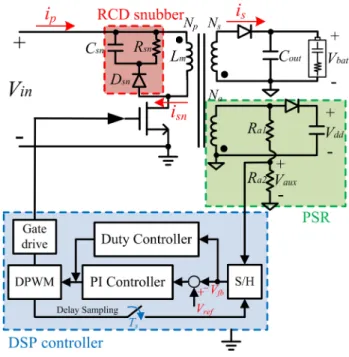
ranges from 100 Vac to 240 Vac, the power adapter for mobile phones nowadays usually include a ac–Dc recti-fier to convert the original high ac voltage up to 240 Vac to 5 V. Succeeding the rectifier is a battery charger, which is expected to offer efficient conversion from 240 Vac to 5 VDc and in compact sizes (Olvitz et al. 2012; cuc-chietti et al. 2011). In this study, a new 0.7a/4.2 V Dc–Dc PSr flyback battery charge system as shown in Fig. 1 is proposed, which consists of a rcD snubber circuit (hren et al. 2006; Sarnago et al. 2013), a PSr flyback converter and a lithium-ion battery. The power switch in this flyback converter is controlled by PWM duty regulation via a DSP module. note that the flyback converter is a common and popular selection for many applications due to its galvanic isolation and wide power range. Flyback converter is made for the galvanic isolation between input and output stage by transformer windings. By adding an auxiliary winding, the output voltage is sensed to assist primary side regula-tion. The topology is an excellent approach in recent years due to its low cost, less components and no temperature limitation.
On the other hand, various techniques to achieve an on-line battery charging have been reported by research-ers. The most common one is the cc/cV method, due to its simplicity and ease to achieve and realize (Fakham et al. 2011; linden and reddy 2001). In this study, the charg-ing system connects a closed-loop controller to achieve rated charging rules, such as cc and cV charge. The con-ventional flyback converter with constant current/voltage applications always requires two sensed aDc channels for
regulating (hou 2010; Tseng et al. 2002; de Sousa et al. 2009; Datasheet 2005, 2008) that are used to sense the input peak current, output voltage or output current to feed-back. This study proposes a duty control method to regulate the output current by only one aDc channel. By this pro-posed control method, the controller of this charging sys-tem is much simpler for implementation.
2.2 charging characteristics of the lithium-ion battery and temperature issues
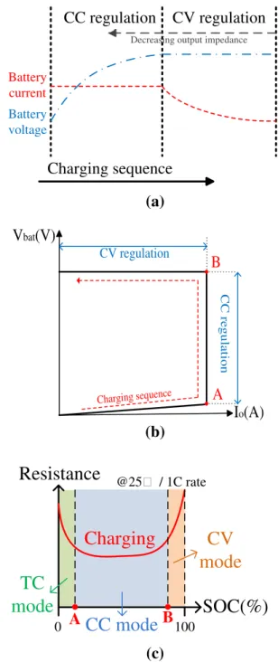
Ideal constant current/constant voltage charging sequences and charge characteristics are shown in Fig. 2a, b (de Sousa et al. 2009). In the beginning of charging, the converter pre-charges the battery until the battery voltage is higher than threshold voltage (point a), then the system switches to the constant current (cc) mode. The charging current is trolled within the rated current value in cc mode. at con-stant current mode, the battery voltage rises rapidly until the battery voltage reaches the maximum rated voltage (point B) and then the system switches to the constant volt-age (cV) mode. at constant voltvolt-age mode, the converter output voltage is controlled within the rated voltage, then the charging current starts to decrease owing to battery load increasing until the charging current is below the rated stop of charge condition.
The safe operating temperature range of the battery is 0–45 °c. The battery impedance affects significantly the battery temperature when battery is charged. The variation of battery impedance corresponds to state of charge (SOc) (andrea 2010), as illustrated in Fig. 2c. It is seen from this figure that the battery impedance is large in the beginning of SOc. Thus, the so-called trickle current charge (Tc) method is used in this interval to reduce the temperature rising in the initial charging period prior to point a. The designed Tc/cc/cV charging method should lead to a favorable performance for the temperature compensation throughout a typical battery charging process.
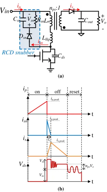
2.3 component design of the rcD snubber circuit
The rcD snubber circuit is shown in Fig. 3a. The exces-sive voltage due to the resonance between Llkp and Cds should be suppressed to an additional circuit in order to protect the power MOSFeT. The rcD snubber circuit in fact absorbs the current in the leakage inductor by turning on the snubber diode (Dsn) when the Vds exceeds Vin plus
npsVo. It should be designed that the sunbber capacitance (Csn) is large enough so that its voltage does not change during a switching period.
When the MOSFeT turns off and Vds is charged to Vin plus npsVo, the primary side current flows to Csn through the snubber diode. Meanwhile, the secondary diode
turns on. Therefore, the voltage across Llkp is equal to the substation of Vsn from npsVo. Then, the slope of isn is as follows,
The time ts can be obtained by
(1) disn dt = npsVo− Vsn Llkp . (2) ts= Llkp Vsn− npsVo ip,peak.
CC regulation CV regulation
Battery voltageCharging sequence
Battery currentDecreasing output impedance
(a)
I
o(A)
V
bat(V)
CC regulation CV regulation Charging sequenceA
B
(b)
Resistance
SOC(%)
0 100 @25 / 1C rateCharging
TC
mode
CC mode
CV
mode
A
B
(c)
Fig. 2 a The cc/cV charging sequences, b the charging characteris-tic, c impedance variation of a battery according to SOc
The power dissipated in the sunbber circuit can be obtained by
On the other hand, since the power consumed in the snubber resister is Vsn2/R
sn, the snubber resistance Rsn can be
obtained by
The snubber capacitance Csn can also be determined by (3) Psn= 1 2Ts Llkpi2p,peak Vsn Vsn− npsVo . (4) Rsn= Vsn Vsn− npsVo Ts 1 2Llkpi 2 p,peak . (5) Csn= VsnIs Rsn∆Vsn ,
where ΔVsn is the voltage ripples on the rcD clamping capacitor. The waveforms pertaining to rcD snubber are shown in Fig. 3(b).
V
in
+
-L
mn
ps:1i
sni
pC
dsC
outV
oC
snR
snL
lkpV
sn+
-D
snRCD snubber
i
s (a) resett
t
t
on offV
dsi
pi
sn ip,peak Vsn Vin npsVo ip,peak ts is,peakt
i
s (b)Fig. 3 a Schematic of a Flyback converter with rcD snubber circuit, b key electronic waveforms of the rcD snubber circuit
reset
t
t
on
off
V
auxV
gs0
2 1 2 ( ) a a o D s a a N R V V N R R 2 1 2 in V a a p a a N R N R R Resonant is caused by magnetizing inductance and switch capacitance. Resonant is caused byleakage inductance.
delay
Sampling
Fig. 4 Schematic waveforms of voltages at selected nodes in a PSr flyback converter
Fig. 5 The flyback converter operated at a on-state, b off-state and c reset state
2.4 component design of the PSr flyback converter The PSr flyback converter as shown in Fig. 1 is proposed to herein replace the opto-coupler in the traditional analog circuit and thus reduce the numbers of feedback compo-nents. The PSr utilizes the auxiliary winding to sense the
output voltage for output voltage regulation. The auxiliary side voltage during the switch-on state is
During switch-off state is obtained by
The auxiliary winding reflects both input and output voltage information in one switching period. In order to regulate the output current and voltage, the output volt-age is an important feedback parameter which needs to be sensed, and then transferred into the controller for regula-tion. however, the output voltage information via the aux-iliary winding is mearable only at off-state. Therefore, the timing of aDc sampling is a key factor in the design of the converter system. Since the battery load consists of a large capacitance, the variation of auxiliary voltage is in small levels. Thus, this study proposes a simpler method for aux-iliary voltage sampling. note that the auxaux-iliary winding can also provide the power for the controller by connecting a diode and a capacitor at auxiliary side. The supplied power of controller is related to turn ratio and determined by
Typical waveforms of PSr flyback converter is shown in Fig. 4. In this figure, the topology of PSr flyback converter provides the sensed voltage signal only. The proposed con-trol method is designed to suit this topology, as stated in the next section. (6) Vaux = Na Np Ra2 Ra1+ Ra2 Vin. (7) Vaux = Na Ns Ra2 Ra1+ Ra2 (Vo+ VD). (8) Vdd = Na Ns (Vo+ VD).
Fig. 6 The key electronic waveforms of the flyback converter in the operations of DcM
Fig. 7 The schematic of the flyback converter with the pro-posed duty control method
The flyback converter is operated in the so-called dis-continuous current mode (DcM), the mechanism of which is shown in details by Fig. 5. In one single switching period, there are three states of operation—on-state, off-state and reset. Figure 5a is the flyback converter operated in on-state. When the switch turns on, the voltage across the magnetizing inductance Lm is the input voltage Vin. Then, the inductor current increases with a slope which is defined by
Figure 5b is the flyback converter which is operated in off state. When the switch turns off, the secondary side diode is conducted, and then the voltage drop of magnet-izing inductance is the output voltage Vo multiplied by
(9) di dt = Vin Lm .
the turn ratio from secondary side to primary side nps. Due to a negative voltage drop across the magnetizing inductor, the inductor current decreases with a slope defined by
Figure 5c shows the magnetizing inductance is in reset. The switch is off and the secondary diode is open because the magnetizing inductance is operated without any energy transfer. Figure 6 shows the waveforms of the primary side current ip, secondary side current is, and the magnetizing inductance current im, when the flyback converter operates in DcM.
The magnetizing inductance should be smaller than the critical magnetizing inductance Lcri, because that the proposed flyback converter operates in DcM, which is (10) di dt = − npsVo Lm .
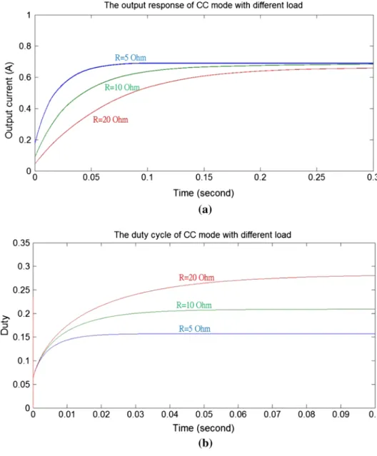
Fig. 8 Dynamic responses of a the output current and b duty cycle correspond to different load conditions by the proposed duty control method
obtained by setting the secondary current isb to zero at the end of off-state in the so-called continuous current mode (ccM). The secondary current can be determined by
where isb is the peak current of the secondary side in ccM. From eq. (11), the critical magnetizing inductance can be determined by
There are some other factors of the flyback converter affecting performance, such as turn ratio and output capaci-tance. The turn ratio is an important design parameter at the primary side to the secondary side, and the ideal turn ratio can be derived from
(11) isb= Io 1 −D− Vo(1 −D) 2Lcri n2 ps fs = 0, (12) Lcri= n2psVo(1 −D)2 2Iofs . (13) nps= Vds,max− Vin Vo+ VD ,
where Vds,max is the maximum voltage across the power MOSFeT. and the turn ratio from secondary side to auxil-iary side can be derived from
where VD_aux is the diode across voltage and the Vdd is the power supply for controller. The output capacitance can be determined by
where the ΔVo is the output voltage ripple, the output ripple is usually expected to be limited within 10 %.
3 The proposed battery charger
The conventional control methods for cc/cV battery charg-ing are voltage and current mode control. The conventional voltage control method is not able to be implemented into the topology of primary side regulation flyback converter, (14) nsa= Vo+ VD Vdd + VD_aux , (15) Co= Io ∆Vo Ts,
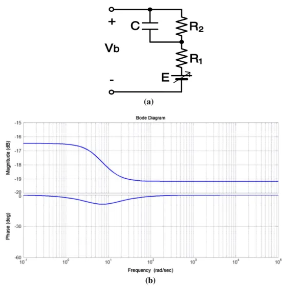
Fig. 9 a The equivalent circuit model of the lithium-ion battery. b Frequency characteristics of the lithium-ion battery (Zhang et al. 1796)
+
Vb
-C
R
2R
1E
(a) (b)since this topology is not capable of sensing the charging current at auxiliary winding side. In the conventional current control method, it needs to consider the noise in primary side peak current caused by the resonance between the cross capacitance of the power MOSFeT and the leakage induct-ance of the transformer. Both conventional methods need two or more aDc channels to process feedback signals. This study proposes a control method which is designed, via sensing the charging current at auxiliary winding side, for the sake of reducing the requirement of aDc channels and simplifying the control algorithms of digital controller. 3.1 constant current regulation by duty control method The conventional control for the constant current mode driving is facilitated by two sensed signals, the output volt-age and current. In order to solve the problems of the com-plex control and peak current noise of the primary side due to switching, an alternate control mechanism is proposed herein with corresponding derivation presented. Based on fundamental formula of the inductor current, the primary peak current can be determined by
where the Don is the duty cycle. The derivation of the pri-mary peak current for conventional current mode control can be derived as
From eqs. (16) and (17), the controlled signal Don can then be derived based on sensed signal Vo by
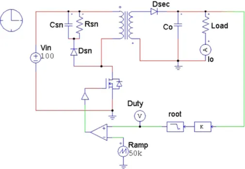
There is only one feedback signal, the output voltage Vo, needed in eq. (18). Following eq. (18), the constant cur-rent regulation can be achieved without curcur-rent sensing. This derivation of the proposed duty control method can be implemented by a simpler controller design for constant current regulation. In this constant current charge, the bat-tery voltage increases as charging current to the batbat-tery. The controlled duty cycle should be increased with out-put voltage rising. The simulation schematic with the pro-posed duty control method is illustrated by Fig. 7 in for-mat of Powersim. The waveforms of the output current and duty cycle with different output loads applied are shown in Fig. 8. From these simulation results, it can be found that the charge current is regulated by controlling duty cycle, while an output constant current is successfully realized.
(16) Ip,peak= VinDonTs Lm , (17) Ip,peak= 2VoIoTs Lm . (18) Don = 2LmIo TsVin2 × Vo.
3.2 constant voltage regulation by a PI controller
3.2.1 Battery model
a typical dynamic model of a lithium-ion battery is shown in Fig. 9a. It consists of the equilibrium potential or open circuit voltage of battery E, lumped internal resistances
R1, R2, and effective capacitance C. The gain-phase plot of battery internal impedance versus frequency is shown in Fig. 9b. It seems that the battery impedance shows the character of a constant resistor is above 10 hz. There-fore, for the frequency range of interest, it is acceptable to model the internal impedance of battery as a constant resistor. replacing the switch components with equiva-lent PWM switch model biased by the operation point of charger, it is got a new equivalent circuit with battery
Rbat at the output of flyback converter. The new set of con-trol to output transfer functions can be obtained for small signal analysis of discontinuous current mode (DcM) condition.
Fig. 10 The PWM switch models. a Voltages and currents model, b average model (Vorperian 1990)
3.2.2 Modeling the switching components for DCM operations
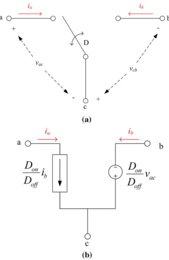
an accurate PWM switch model provides a simple and straightforward method to analyze the small-signal char-acteristic of switching converters. The invariant relation-ship between the terminal currents and voltages of the PWM switch is applied in a flyback converter as shown in Fig. 10a. The average terminal currents and volt-ages of small-signal model are derived by (Vorperian 1990)
By eq. (19), Doff, ia and vac could be derived as follow, (19) ia= ip,peak 2 Don,ib= ip,peak 2 Doff, vac= L ip,peak DonTs ,vcb= L ip,peak DoffTs .
The average model of PWM switch in DcM could be re-described as in Fig. 10b by eq. (20). a correspond-ing small-signal model with flyback converter can be obtained from the relationship among the perturbations in average terminal quantities at a given dc operating point (Ib, Vac, D). equations (19) and (20) can be com-bined by
where the parameters are defined by
(20) Doff = 2LFs Don ia vcb =2LFs Don ib vac ,ia= Don Doff ib,vac= Doff Don vcb. (21) ˆia= ˆvac ri + kidˆon, (22) ˆib= gfˆvac+ kodˆon− ˆvac ro ,
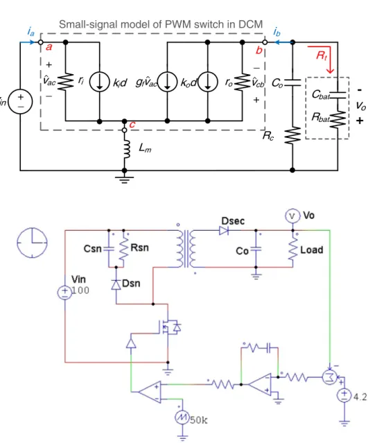
Fig. 11 The small signal model of the flyback converter with the battery load in a discontinuous current mode +_ Lm
-v
o+
v
in Co ri Rc Cbat vac _ + kid gfvac kod ro Rbat RtSmall-signal model of PWM switch in DCM
ia ib a b c vcb _ +
Fig. 12 The schematic of the flyback converter with a PI controller
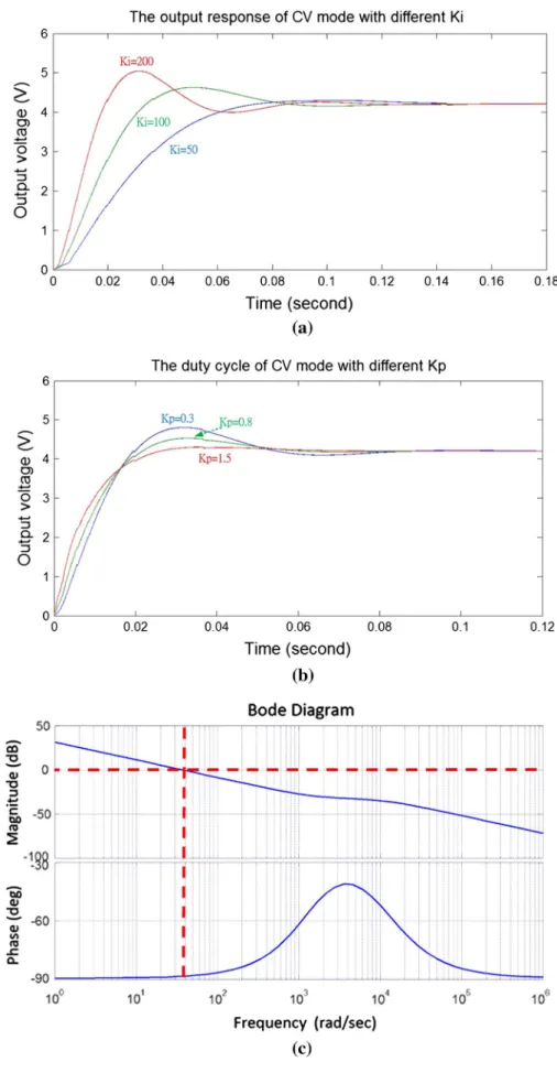
Fig. 13 Step responses of a different parameter values of ki, and b different parameter values of kp with ki = 200, c frequency response with PM −90°
equations (21) and (22) result from current balance at the block prescribed by node a, b and c in the small-signal equivalent circuit of Fig. 11. The small signal model can be derived around the operation point of the state on the charge profile. The control of output transfer function for DcM operations is derived from (Vorperian 1990)
where Hd is the dc gain of flyback converter; sz1, sz2 are the first and second zeros; sp1 is the dominate pole which is determined by output impedance and output capacitance;
sp2 is the second pole which is at a higher frequency. The dc gain of the flyback converter can be derived as
The zeros and poles can also be derived as
(23) ri = Vac Ia ,ki= 2Ia Don , (24) ko= 2Ib Don , ro= Vcb Ib , gf = 2Ib Vac . (25) vo(s) d(s) = Hd 1 + s sz1 1 + s sz2 1 +ss p1 1 +ss p2 , (26) Hd= 2vo D 1 + Rt Rbat . (27) sz1= 1 RcCo , sz2 = Rt M(1 + M)Lm , sp1= 1 Co(Rbat+ Rc) , sp2= Rt(Rbat+ Rc) Lm(M + 1)2Rbat , Constant current charge Trickle charge Start Vbat<3 Vbat=4.1? yes no yes Detecting battery voltage no Constant voltage charge Ibat<0.04c no End of charge yes
Fig. 14 The flowchart of overall charging procedure Table 1 The specifications of the lithium battery considered
Items Specifications
nominal capacity 1,400 mah
nominal voltage 3.7 V
Final charge voltage 4.2 V
cut-off voltage 3.0 V
Standard charge current 0.7 a
Final charge current 0.028 a
Internal resistance <70 mΩ
Operating temperature 0–45 °c
Fig. 15 experimental system of the proposed PSr flyback battery charger
where M is the voltage conversion ratio from input to out-put which is defined by
The variable Rt = Vo/Io is the output impedance for a
resistive load or battery load in the DcM transfer function. a PI controller is a common selection to reduce the steady-state error (ess) as below
It is known that kp is selected for fast transient response and ki is selected for small steady-state error. The circuit topology for simulation on the flyback converter with PI controller is shown in Fig. 12. The ki is chosen as 50, 100 and 200 first where the step response is shown as Fig. 13a. It is seen that the response speed is obviously proportional to ki and the best response is the one with the 200. however, there is an overshoot phenomenon in transient response. The kp is designed for eliminating overshoot and reducing rise time.
kp is chosen as 0.3, 0.8 and 1.5 for step responses. It can be observed from simulation results in Fig. 13b that the phe-nomenon of overshoot can be eliminated with kp = 1.5 while keep fast response speed. Based on these simulation results, the parameters of the adopted PI controller for cV compen-sation are ki = 200 and kp = 1.5. note that the ranges of ki
and kp considered herein is chosen to cover the possible best performance of the controller. The finally-chosen ki = 200 and kp = 1.5, as shown in Fig. 13c for frequency response, could lead to a phase margin close to 90°. The results clearly show that PI controller compensates well the system for fast transient response, precise steady response and stability. 3.3 Sampling method of auxiliary side voltage
The sensed auxiliary voltage varies slightly as well dur-ing off-state. It follows that the timdur-ing of sampldur-ing is an important part of this study to obtain the correct feedback voltage (Datasheet 2005; chang 2009). The adopted sam-pling method on the sensed auxiliary voltage is a specific delay sampling approach for two different charge modes. The auxiliary voltage can be well sensed first by off-line tests with different duty cycles at two charge conditions, constant current (cc) and constant voltage (cV) charges.
The observed results are given as follows. The duty cycle of the cc charge is about 15–20 %, which is orchestrated the mechanism given eq. (18). The observed delay time of the auxiliary voltage can be sampled is 3–7 μs. In the cV mode, the duty cycle is from 20 to 10 %, while the observed delay time of the auxiliary voltage is sampled is about 2–4 μs based on eq. (18). The delay time of auxiliary voltage sampling is in fact determined by different duty cycles and
(28) M = vo vin . (29) C(s) = kp+ ki s.
charge modes. note that in DSP implementation, the sam-pling is triggered by aDc interrupts which are determined by summing duty cycle and the delay time pre-designated. In results, it is obvious that the auxiliary voltage can be sensed much precisely by this way. Typical waveforms of switch terminal voltage and auxiliary voltage as the proposed delay sampling method applied are shown in Fig. 4.
4 Experiment results
4.1 Flowchart of digital charging system
The flowchart of overall charging procedure is shown in Fig. 14. an aDc channel senses the battery voltage to offer feedback to the system with the aim to decide and switch between different charge modes. The trickle charge mode is adopted when battery voltage is under 3 V. The constant
PWM1
PWM2
V
auxT
delay (a) PWM1 PWM2 Vaux Tdelay (b)Fig. 16 Delay sampling waveforms with a cc mode (heavy load condition) and b cV mode (light load condition)
current charge mode is applied when voltage is between 3 and 4.1 V. The constant voltage charge mode is on when battery voltage is getting 4.1 V. The charging process ends as the charging current is under 0.04 c.
4.2 Battery operations
a signal cell 18,500 type battery is used for implementa-tion, which is made from the company eanTeK. The characteristics of this rechargeable lithium battery are given in Table 1. The maximum rated charging current is regulated at 0.7a (1 c) while the cut-off voltage is 3 V. It is set that 0.7 a for designed charging current while 4.2 V for designated cV regulated voltage to achieve safe and fast charging processes. The timing for the stop of charge is set as the charging current decreases to 0.028a (0.04 c). By eq. (18), the charge current 0.028a is modified to duty cycle about 3 %. In the other words, the cV charge mode stops when the duty cycle is under 3 %.
4.3 experiment results
The experiment system consists of a 0.7a/4.2 V Dc–Dc DcM flyback converter circuit designed and realized in the laboratory. This is designed for charging opera-tions on a 100 V Dc-line and 1,400 mah lithium-ion battery, a temperature sensor aD595 and a DSP module (TMS320F2812), as shown in Fig. 15. The nominal output
Vo is set as 4.2 V for the constant voltage charging mode; the switching frequency fsw is 50 khz; the magnetizing inductance Lm is 500 μh; and the leakage inductance Llkp is 30 μh; the output capacitance Co is 680 μF. The turn ratio of the transformer between primary, secondary, and auxiliary windings np:ns:na, is 100:10:20. The DSP senses two signals, the voltage across the auxiliary winding and the battery temperature from aD595.
The experimental results of delay sampling for different charge conditions are shown in Fig. 16. The delay time of sampling is modulated by duty cycle and charge mode. The
Fig. 17 completed waveforms of a charging sequence, and b temperature variations with different charging methods
delay time of cc mode and cV mode are about 5 and 3 μs, respectively. The auxiliary voltage is sensed at positive-edge-triggered of PWM2. The experiment result of the pro-posed battery charging system is shown in Fig. 17a, where the charge current is driven at 0.2 and 1 c for Tc and cc modes, respectively. The overall charging sequence lasts for about 130 min, where the Tc, cc and cV charging periods about 10, 37 and 83 min, respectively. The accuracy of the proposed cc regulation is successfully lowered to 7 %. To compare the proposed charging method with con-ventional cc/cV method, it is seen that only 1 °c-rise in Tc mode and the total temperature rise is 7°cwith the pro-posed charge method. It is better than conventional cc/cV method (14 °c) as Fig. 17b. To explore repeatability, many experiments are conducted and the results generally show that the proposed PSr flyback charging system with the charge algorithm is capable of minimizing the temperature rise of battery charging and implementing cc and cV effi-ciently to be within around 7 °c.
Finally, conversion efficiency is explored. The efficien-cies for the different loads are shown in Fig. 18. There are two cases of flyback converters with the designed charg-ing algorithm, rcD snubber and active-clamp, where the active-clamp flyback converter is designed to achieve the zero voltage switching (ZVS) to increase efficiency. The best efficiency of the active-clamp flyback converter is about 60 %. It is better than the rcD snubber flyback con-verter (55 %). These results are all with Tc mode activated. 5 Conclusion
a new flyback Dc–Dc converter responsible for charg-ing a rechargeable lithium battery is proposed in this study.
The accompanying proposed battery charging method is implemented by a digital controller. an improved control method is proposed in this study to achieve cc/cV by only one aDc channel. This study presents a battery charge mechanism with a flyback converter and the associated trickle charge method, which is particularly effective for the temperature compensation. The PSr is adopted for esti-mating output currents which are then used to determine the switchings between Tc, cc and cV modes. The Tc charging method is used to avoid the rapid increase in the temperature of the battery. The designed flyback converter with proposed control method is simulated by the soft-ware Powersim. It is clearly shown that the cc/cV can be achieved by only outputing voltage feedback, which is also proven in a much simpler circuit with the designed con-trol method as compared to conventional cc/cV methods. experiments are successfully carried out to validate the expected performance of the designed battery charger and the PSr flyback converter. It is shown that the Tc/cc/cV charging is well achieved with the proposed duty control method and PI control. The deviation of the rated output current is successfully limited 7 %, while the temperature can be contained effectively within 7 °c with the designed charging method. Furthermore, the designed converter achieve an efficiency of 60 % better than some reporteds. The proposed PSr flyback converter with the designed bat-tery charger is proven effectively for batbat-tery charging and temperature compensation.
Acknowledgments The authors appreciate the support from national chip Implementation center and national Science council of r.O.c under the grant no. nSc 101-2221-e-009-165. This work was also supported in part by the UST-UcSD International center of excellence in advanced Bio-engineering sponsored by the Tai-wan national Science council I-rice Program under the grant no. nSc-101-2911-I-009-101.
References
andrea D (2010) Battery management systems for large lithium-ion battery packs, 1st edn. (online). available at: http://www. lib.nctu.edu.tw/
chang c-W (2009) Digital primary-side sensing control for flyback converters. MS thesis, Institute of ee, ncTU, hsinchu
chen BY, lai YS (2012) new digital-controlled technique for battery charger with constant current and voltage control without current feedback. Ieee Trans Ind electrons 59:1545–1553
chen Th, lin Wl, liaw cM (1999) Dynamic modeling and control-ler design of flyback converter. Ieee Trans aerosp electron Syst 35:1230–1239
chen lr, chu nY, Wang cS, liang rh (2008) Design of a reflex-based bidirectional converter with the energy recovery function. Ieee Trans Ind electron 55:3022–3029
cucchietti F, Giacomello l, Griffa G, Tecchio P, Bolla r, Bruschi r, D’agostino l (2011) environmental benefits of a universal mobile charger and energy-aware survey on current products. InTelec 2011:1–9
Datasheet (2005) iW2202: Digital SMPS controller. iWatt Inc., camp-bell. http://www.datasheet-pdf.com/datasheetdownload.php?id= 706706
Datasheet (2008) an-6067: design and application of primary-side regulation (PSr) PWM controller. Fairchild Inc., San Jose. http://www.dzsc.com/uploadfile/company/123460/20104823395 2699.pdf
de Sousa GJM, cruz cMT, Branco cGc, Bezerra lDS, Torrico-Bascope rP (2009) a low cost flyback-based high power factor battery charger for UPS applications. Ieee cOBeP conf, pp 783–790
Do Valle B, Wentz cT, Sarpeshkar r (2011) an area and power-effi-cient analog li-ion battery charger circuit. Ieee Trans Biomed circuits Syst 5:131–137
Fakham h, Di l, Francois B (2011) Power control design of a battery charger in a hybrid active PV generator for load-following appli-cations. Ieee Trans Ind electron 58:85–94
hou h-c (2010) Power factor correction of DSP-based flyback isola-tion converter for positive/negative pulse lithium battery charger. MS thesis, Institute of ee, nSYSU, Kaohsiung, 2010
hren a, Korelic J, Milanovic M (2006) rc-rcD clamp circuit for ringing losses reduction in a flyback converter. Ieee Trans cir-cuit Syst Soc 53:369–373
hsieh Yc, huang cS (2011) li-ion battery charger based on digitally controlled phase-shifted full-bridge converter. IeT Power elec-tron 4(2):242–247
hua cc, hsu ch (2005) Implementation of a regenera-tive pulse and equalization battery charger using a DSP. Ieee PeDS conf, pp 955–959
hwang Y-S, Wang S-c, Yang F-c, chen J-J (2007) new compact cMOS li-ion battery charger using charge-pump technique for portable applications. Ieee Trans circuits Syst I 54:705–712 Kleebchampee W, Bunlaksananusorn c (2005) Modeling and control
design of a current-mode controlled flyback converter with opto-coupler feedback. Ieee PeDS conf, pp 787–792
li Y, Zheng J (2010) a low-cost adaptive multi-mode digital con-trol solution maximizing ac/Dc power supply efficiency. Ieee aPec conf, pp 349–354
lin FJ, huang MS, Yeh PY, Tsai hc, Kuan ch (2012) DSP-based probabilistic fuzzy neural network control for li-ion battery charger. Ieee Tran Power electron 27(8):3782–3794
linden D, reddy TB (2001) handbook of batteries, 3rd edn. McGraw-hill, new York
Olvitz l, Vinko D, Svedek T (2012) Wireless power transfer for mobile phone charging device. MIPrO 2012:141–145
Paul cP, chao WD, chen, cheng cW (2013) a fast charging algo-rithm for an intelligent PV system with capability of on-line tem-perature compensation. Microsyst Technol 19:1289–1306 Sarnago h, lucia O, Mediano a, Burdio JM (2013) Series resonant
inverter with active snubber circuit for improved efficiency oper-ation applied to domestic induction heating. Ieee aPec2013 conf, pp 1584–1589
Thang TV, Thao nM, Jang J, Park J (2013) analysis and design of grid-connected photovoltaic systems with multiple-integrated converters and a single-phase pseudo Dc-link inverter. Ieee Trans Ind electron (online published)
Tseng Kc, liang TJ, chen JF, chang MT (2002) high frequency pos-itive/negative pulse charger with power factor correction. Ieee PeSc conf, pp 671–675
Vorperian V (1990) Simplified analysis of PWM converters using model of PWM switch II. Discontinuous conduction mode. Ieee Trans aerosp electron Syst 26:497–505
Zhang W, Skelton D, Martinez r (2004) Modeling and analysis of an off-line battery charger for single cell lithium batteries. Ieee aPec conf, pp 1796–1802