ELSEVIER Thin Solid Films 346 (1999) 269-274
Analysis of AC electrical response for radio-frequency sputtered
(Ba&&)Ti03
thin film
Yin-Pin Wang, Tseung-Yuen Tseng”’
Depatment of Electronics Engineering and Institute of Electrobcs, National Chiao-Tmg Universiy, Hsinchu, Taiwan Received 30 December 1997; accepted 17 October 1998
Abstract
Through the measurement of dielectric dispersion as a function of frequency (100 Hz <f 5 1 MHz). we investigated the trapping dielectric relaxation of r.f.-sputtered (Ba&r,jS)TiOJ film and proposed an equivalent circuit on the basis of the admittance and capacitance spectra. Admittance spectral studies in the temperature range of 200-420 Krevealed the existence of a trap level. The trap, located at 0.05 eV? is envisaged to be responsible for the origin of dielectric relaxation and carrier concentration. The equivalent circuit, consisting of a series trapping resistance and capacitance combination in parallel with leakage resistance and high frequency limit capacitance, is adopted to explain satisfactorily the AC response and to identify the contribution of the shallow trap on the electrical properties of BST thin film. 0 1999 Elsevier Science S.A. All rights reserved.
Kqw~ords: Barium strontium titanate oxide (BST); Dielectric response: Impedance; Cole plot
1. Introduction
At present, ferroelectric films are we11 recognized to be excellent capacitor materials for dynamic random access memory (DRAM) in ultra large scale integration [l]. The most attractive advantage in ferroelectric materials over the conventional nitride-oxide is that the former have a very high dielectric constant, especially for memory densities higher than 64 Mb and above. Among those ferroeletric
films, barium strontium titanate oxide (abbreviated BST) is a promising material candidate for DIXM because of its paraelectric phase, high dielectric constant and low temperature coefficient of capacitance. Although many arti- cles on the electrical properties of BST films have been published, they primarily focused on a single-frequency test, which is typically selected at 1 k [2-71, 100 k [8,9] or 1M Hz [lo]. This kind of evaluation is appropriate for a defect-free single crystal material. It is commonly concluded [ 1 I-151 that the Pt/BST junction has Schottky- barrier rectifying properties. The electrons trapped at the
interface sustains the Schottky-barrier and are compensated
by positive-ionized shallow donors within the depletion region. Hence, the heterogeneity, resulting from the defect or impurity in the contact or grain, often leads to a dielectric
* Corresponding author. Tel.: + 886-35-731879; fax: f 886-35- 724361.
E-mail address: [email protected] (T.Y. Tseng)
relaxation as a function of frequency in Pt/BST/Pt capaci- tors. The dielectric relaxation greatly affects the electrical properties of the BST capacitor, such as field-stress leakage current [ 151, stored-charge loss [16] and pause refresh prop- erties [17]. The dielectric relaxation can be analyzed over a wide range of measurement frequency and temperature. Takamura [ 181 and Watnable et al. [ 191 have, respectively, investigated frequency-dependent dielectric response for
Ru02/BST and RuOJPZT capacitors, but the origin and
role of dielectric relaxation in BST capacitors still remain unclear.
In this study, we employed the admittance spectroscopy and complex planes technique to identify the AC electrical response of polycrystalline Pt/BST thin film capacitors. The admittance spectroscopy is verified to be a useful method for detecting fast or shallow trap levels [20]. The complex plane analysis is another powerful tool used for characteriz- ing the dielectric response of heterogeneous polycrystalline materials, such as BaTiO:, ceramics [21,22], ZnO varistors 11231, transparent conductors [24], and ferroelectric ceramics 125,261. An equivalent circuit is required in this complex plane technique to provide realistic representation of experi- mental AC data of the polycrystalline film. Complex admit- tance (Y*), impedance (Z*) and capacitance (C*:) plots are three useful electrical parameters for characterizing the AC response of the film. When the AC data are systematically transformed into two or more complex planes [22,27,28],
0040-6090/99/$ - see front matter 0 1999 Elsevier Science .%A. All rights reserved. PII: SOO40-6090(98)01497-7
170 Y.P. Wang. T.Y. Tseng / Thin Solid Films 346 (19991269~274
the appropriate equivalent circuit can be usually possible to identify. The purpose of this paper was to probe shallow defects using admittance spectroscopy and to propose a realistic equivalent circuit by three complex planes (impe- dance, admittance and capacitance) analyses so that the effect of dielectric relaxation on the electrical properties of BST film can be better understood.
2. Experimental procedure
The n-type (100) silicon wafer was cleaned by standard process. The SiO? layer was thermally grown in a furnace for obtaining a film thickness of 300 nm. The 100-m-n thick Pt bottom electrode was deposited on the Si02 layer by an electron-gun. BST thin films on the bottom electrodes were deposited by r.f.-sputtering at a substrate temperature of 500°C. The sputtering gas consists of 50% Ar and 50% 01 mixture with a total pressure of 10 mTorr. The film thick- ness was estimated to be 90 m-n by using a Tencor Alpha- Step 200 profilometer. The Pt top electrodes with a thick- ness of 50 nm and diameters of 350 Frn were patterned by the shadow mask process. The result of inductive coupled plasma analysis indicated that the BST thin films were composed of 50% Ba and 50% Sr. X-ray diffraction analysis indicates that the film belongs to the pervoskite cubic phase. The sample was mounted in a continuous flow liquid nitro- gen cryostat capable of controlling the temperature of i 1-K between 150 and 420 K. The AC electrical response of the BST films was monitored with a computer controlled impe- dance analyzer (HP4194A). The AC electrical data, in the form of parallel capacitance (C,) and conductance (G,), were recorded in the frequency range of 100 Hz to 1 MHz at an AC signal amplitude of 0.1 V.
2 s
102 103 104 105 18
Frequency (Hz)
Fig. 1. Frequency dependence of relative real dielectric constant (Ed’), imaginary dielectric constant (Ed”) and loss tangent (tana) at T = 300 K.
Et = 0.05 eV
ig4
2 3 4 5
IooOrr (d)
Fig2 (a) G/w(~C”j as a function of frequency at various temperatures. Cbi An Arrhenius plot of 1nwdT’ versus liTfor obtaining the trap activation energy.
3. Results and discussion
The admittance (I’*) and impedance {Z?) can be defined in an expression relating the electrical current and applied voltage
Z(w) = Y”(w)V(w) = .P(w)-‘V(0) (1)
For the purpose of this work. a complex capacitance plane is expressed as the following equation
c*(o) = Y”(w)/jo =Re(C”) -jZm(C”~= C”( &:--j&y)
where w is the angular frequency, C,, the geometric capaci- tance in free space. C, and G, the equivalent parallel capa- citance and conductance of entire circuit. respectively. Fig. 1 depicts the variation of relative real dielectric constant (E,‘), imaginary dielectric constant (E,“) and loss tangent
Y.P. Wang, T.Y. Tseng / Thin Solid Films 346 (1999) 269-274 271 0
200
400
600
800
Re[Z*] (M R)i---l
- r _ 0 - rt= cop -‘= 0.11 ms E’2: \ ii350
0 0 20 2040
40
60
60
ReVI (PS)
ReVI (PS)
Fig. 3. (a) Complex impedance plot (Z*) of BST film at T = 300 K. (b) Complex capacitance plot (C*) of BST Elm at T = 300 K. tc) Complex admittance plot (I’+) of BST Elm at T = 300 K. The inset plot is the corresponding expanded section near the origin, from which we can deter- mine the I&( = YG).
(tan6 = E,‘/E,“) with frequency at T = 300 K. The Ed’ drops from a high value ~;f: at low frequency to a low value E,,,’ at high frequency, and the curve has an inflection point, which was reported to be located near the emission rate of a trap [29]. Both E,“(W) and tana have peak values at a frequency of about 1.4 kHz. The frequency dependence of tam?(w) is the same as that of E,“(W). The conductance G of a Schottky junction can be described as a sum of the trap conductance G, and DC component Gnc [29?30], i.e.
G(w, T) = G,,(T) + G,(w, T) (3)
By applying a small AC signal at a given temperature, the peak of G(o)/w occurs when the angular frequency of the AC signal equals the emission rate (e,) of electrons in a trapping state [29,30], i.e.
where wP denotes the peak frequency, cr, the capture cross section of the trap, “!h the free electron thermal velocity, and N, the effective conduction band density of state. Since &his varied with T’” and N, has a T”’ dependence, a plot of ln(w@) versus l/T enables us to determine a trap activa- tion energy E,. Fig. 2a displays the plots of G/o versus w at various temperatures. We found that wP shifts to higher frequency with increasing temperature. A shallow trap was evaluated to be 0.05 eV on the basis of an Arrhenius plot shown in Fig. 2b. Using I-V analysis of BaTiOj-based multilayer capacitors, Lee et al. [31] found that the activa- tion energy is 0.162 eV for the ohmic current and 0.107 eV for the space charge Limited current. The space charge limited current is proportional to the mobility of the carriers. In comparison, the ohmic current is proportional to both mobility and native carrier concentration. The result revealed that the native carrier concentration activation energy was equal to 0.055 eV [31], which is consistent with the present experimentally determined trap activation energy. Thus, the observed shallow trap level would be one of the defects which are responsible for the carrier concen- tration and AC dielectric relaxation of BST films.
Fig. 3a-c, respectively, displays three complex plane plots of the .4C data at T = 300 R, including impedance (Z*), capacitance (P) and admittance (Y*). These Z* and Y* complex quantities can be expressed in terms of G, and CP
z*(w) = Re(Z”) - jh(Z*) = R, - j-$ (5) s
Y*(W) = Re(Y*) +jh(Y*) = G, -I- joCp (6)
R, =
6
G; + c.?C; (7)
172 Y.P. Wang, T. Y. Tseag / Thin Solid Films 346 (19991 269-274
Fig. 4. The schematic equivalent circuit model for BST capacitor.
0 ~‘l~~~‘~ll~‘~~l~‘~t~J’~~i~ 0.0 0.2 0.4 0.6 0.8 1.0 Frequency (MHz) 0* 0.0 0.2 0.4 0.6 0.8 1.0 Frequency (MHz)
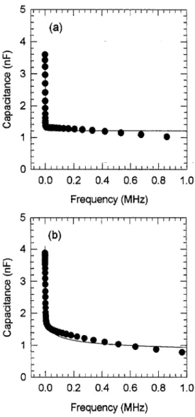
Fig. 5. (a) The measured Lsymbol) and calculated (line) capacitance plot at 7 = 200 K. (b! The measured (symbols) and calculated [line) capacitance plot at 7 = 300 K.
n T=3OOK
0 1 2 3 4 5
Re [Cl (nF)
Fig. 6. The Cole-Cole plots of com$ex?apncitance forB-STZl-m at variius temperatures.
The impedance Z* corresponds to a parallel R-C circuit. On the other hand. a semicircular fit of the AC data in the complex C* planes (Cole-Cole plot) suggests an series equivalent R-C circuit that represents the observed spectra. The impedance (Z*) data in Fig. 3a lie on a single arc, and do not form a distinct semicircle. Hence, the parallel R-C combination appears to be an unsatisfactory representation of AC response for our frequency range. On the contrary, the emergence of a semicircular plot in a complex c=ci- tance plane (Fig. 3b) indicates that a series R-C combina- tion with a relaxation time (7, = 0.11 ms) can equally represent an AC response of the BST film. In the complex Y* plane (Fig. 3c), the curve approaches the semicircle as the measured frequency tends to zero. A switching between the C* and P planes is in agreement with the observation reported by Grant [27]. On the basis of C* and r* planes analyses [27], we proposed a practical equivalent circuit for BST capacitors, as shown in Fig. 4. The C, represents the high frequency capacitance due to the depletion region and Rot shows the low-field leakage resistance. The equivalent circuit in Fig. 4 also includes the contribution of a shallow trap (E, = 0.05 eV) whose characteristic time constant, r,(T) = R,(T) X C,(T), gives rise to a conductance peak
when w = l/7,. The C, value can be determined by subtract- ing left and right intercepts on a semicircular relaxation in real C* axis. R, can be derived from the measured wP (R, = lIC,wr) and RDc is equal to a reciprocal of the left intercept on the real Y* axis [27]. The C, calculation can be described as the following: Supposing-that the observed frequency dependence of capacitance was attributed to the dielectric after-effect, Clf, could be written as Ccf, = C,,-+ Co Xf”-’ [15.32], where C, denotes the capacitance at
high-frequency and C,, the capacitance due to dielectric relaxation. By fitting this equation into our measured data, we found that Ccf, is L .2 + 90 Xf-“” (nF) at T = 200 K and
0.37 + 10.6 Xf-“” (nF) at T = 300 K (see Fig. 5a,b). Fig.
Y.P. Wang, T.Y. Tseng / Thin Solid Films 346 (1999) 269-274 273
Table 1
Measured and calculated parametric values of the equivalent circuit shown in Fig. 4 extracted from analyses of the (C*) and (I’*) planes at various temperatures.
Temperature IK) C, (nF) R, (R) wp (radk) C, (nF) RDc (0) 0”
2cx) 2.7 231 k 1.6 k 1.2 25 M 2 230 2.7 132 k 2.8 k 1.1 25M 6 260 2.6 68.7 k 5.6 k 0.88 25M 9 300 2.5 44.5 k 9.0 k 0.37 25M 10 340 2.3 28.9k 15 k 0.06 2.5hf 11 420 2.2 15.ik30k - 25M 11
planes at various temperatures. On the basis of the above described concept and procedure, we extracted the related parameters of the equivalent circuit as indicated in Fig. 3 at various temperatures and list them in Table 1. C, at
T =
420 K is difficult to calculate because of strong capacitance dispersion.
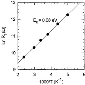
R,
shows an Arrhenius-type temperature depen- dence and its activation energy was calculated to be 0.08 eV, as shown in Fig. 7.Rot
remains constant until 320 K and both C, and C, decrease as temperature is increased (see Fig. 8). The peak frequency is rather inversely proportional toR,
than C,. The depression angle 0 of a semicircular response in a C* plane is defined when the center of a semicircle lies below the x-axis instead of on the x-axis, as illustrated in Fig. 3b. Here we obtain the 0 values on the basis of the measured data indicated in Fig. 6 and the non-Debye empirical relation reported in Ref. [33]. The non-zero value of 0 has been reported to correspond to the distribution of relaxation time [33] and reflects the degree of uniformity in the conductance relaxation. Joncher [34] showed that 8 is related to the extent of the screening effect caused by the hopping charges when it cannot follow the changes of the polarization brought about by an alter- nating electric field. The value of 6 increases as the temperature increases (see Fig. 8) because of a large number2
3
4
5
6
1000/T (K-l)
Fig. 7. An Arrhenius plot of trapping resistance as a function of reciprocal of temperature.
:
8
3
65
&
4rn
2
ODO200
300
400
Temperature (K)Fig. S. Temperature dependence of the trapping capacitance, high- frequency capacitance and depression angle.
of free carriers whose motion is dominated by discontinuous hops and cannot be followed by an immediate readjustment [23]. Taking account of a dynamic random access memory application, the dielectric relaxation would result in less than 10% loss of storage charge during the refresh cycle and hence the film’s DC leakage less affects the device operation [ 161.
4. Conclusions
In this paper, we studied the dielectric relaxation of BST films in the frequency range of 100 Hz to 1 MHz. The dielectric relaxation arises from a shallow trap
(E, = 0.05
eV), which is detected by the admittance spectra carried out at various temperature (200 5
T
5 420 K). This trap also plays an important role in the contribution of the dielectric loss and carrier concentration. In order to qualify the trap- ping effect on the capacitance and admittance, we proposed an equivalent circuit that consisting of a series trapping resistance and capacitance combination in parallel with DC resistance and high frequency limit capacitance. This equivalent circuit model can provide a viable mean by which processing variables can be expected to be related to BST electrical properties.Acknowledgements
This work was supported from the National Science Council of R.O.C. under project no. NSC 86-2112-MOO9-
028.
References
[l] T.Y. Tseng, Proc. 1996 Int. Electron Devices and Materials, C 2-5 National Tsing Hua University, Hsinchu. Taiwan, 1996, p. S9.
274 Y.P. Wang, T.Y. Tseng / Thin Solid Films 346 119991 269-274
[2] S.O. Park, C.S. Hwang, H.J. Cho, C.S. Kang, H.K. Kang, S.I. Lee, M.Y. Lee. Jpn. J. Appl. Phys. 35 (1996) 1548.
[3j T. Kawahara. M. Yamamuka, A. Yuuki, K. Ono, Jpn. J. Appl. Phys. 35 (1996) 4880.
141 N. Ichinose. T. Ogiwara. Jpn. J. Appl. Phys. 34 (1996) 5198. [S] D.M. Tahan, A. Safari, L.C. Klein, J. Am. Ceram. Sot. 79 (1996)
1593.
[6] N. I&nose, T. Ogiwara, Jpn. J. Appl. Phys. 32 (1993) 4115. [7] C.S. Hwang, S.O. Park, H.J. Cho, C.S. Kang, H.K. Kang,-S.I. Lee,
M.Y. Lee. Appl. Phys. Lett. 67 (1995) 2819. [S] K. Abe, S. Komatsu, Jpn. J. Appl. Phys. (1994) 33. [9] K. Abe, S. Komatsu, Jpn. J. Appl. Phys. (1996) 5297.
[lo] L.A. Knauss. J.M. Pond, J.S. Horwitz, D.B. Chrisey, C.H. Mueller, R. Treece. Appl. Phys. Lett. 69 (1996) 25.
[l l] C.S. Hwang, B.T. Lee, H.J. Cho, K.H. Lee, C.S. Kang. H. Hideki, S.I. Lee, M.Y. Lee, Appl. Phys. Lett. 71 (1997) 371.
[12] MS. Tsai, S.C. Sun, T.Y. Tseng, J. Appl. Phys. 82 (1997) 3482. [13] S. Dey, J.J. Lee, P. Alluri, Jpn. J. Appl. Phys. 34 (1995) 3142. [14] J.F. Scott, Integr. Ferroelectr. 9 (1995) 1.
[15] Y. Fukuda. K. Numata, K. Aoki. A. Nishimura, Jpn. J. Appl. Phys. 35 I 1996) 5178.
[16] T. Horikawa, T. Makita, T. Kuroiwa, N. Mikami, Jpn. J. Appl. Phys. 34 11995) 5478.
[17] R. Waser, Science and Technology of Electroceramic Thin Films, in: 0. Auciello. R. Waser (Ed%), NATO AS1 Series, 284, Kluwer Academic Publishers, Dordrecht, 1995, p. 323.
1181 K. Takemura. S. Yamamichi. P.Y. Lesaicherre, et al.. Jpn. J. A&. Phys. 34 (1995) 5224.
[19] K. Watanabe, J.F. Tressler, M. Sadamoto, C. Isobe, M. Tanaka, J. Electrochrm. Sot. 143 (1996) 3008.
[20] D.L. Losee, J. Appl. Phys. 46 (1975) 2X4.
[21] C.H. Lai, T.Y. Tseng, IEEE Tram, Comp. Packing Manuf. Technol. A. 17 (1994) 309.
[22] D.C. Sinclair. A.R. West, J. Appl. Phys. 66 (1989) 3850. [23] S.N. Bai, T.Y. Tseng, J. Elec.Mater. 21 jlq92) 1073,
[24] A.E. Desouza. S.H. Monteiro. C.V. Santilli. S.H. Pulcinelli. J. Mater. Sci: Mater. EIectr. 8 (1997) 259.
1251 S. Bu. A. Chun, G. Park, J. Appl. Phyb. 82 (1997) 2528. 1261 M. Yokosuka. Jpn. J. Appl. Phys. 34 (1995) 5338. [27] F.A. Grant, J. Appl. Phys. 29 (1958) 76.
[28] J.E. Bauerle, J. Phys. Chem. Solids 30 (1969) 2657.
[29] J. Barbolla. S. Duenas, L. Bailon. Solid-State Electron. 35 (1992) 285. [30] G. Vincent, D. Bois, P. Pinard, J. Appl. Phys. 46 (1975) 5173. [31] H.Y. Lee. KC. Lee, J.N. Schunke, L.C. Burron, IEEE Trans, Comp.
Hybrid Manu. Technol. 7 (1984) 443.
[32] Y. Inuishi, T. Nakajima, K. Kawabe, M. Ieda. in: D. Gakkai (Ed.), Yudentai Genshoron (Dielectric Phenomenology), Ohmsha, Tokyo, 1973, pp. 349 (in Japanese).
1331 K.S. Cole, R.H. Cole. J. Chem. Phyb. 9 (1941) 341. 1341 A.K. Jonker. Phys. Status Solidi A 32 (1975) 665.