國 立 交 通 大 學
光電工程研究所
博 士 論 文
成長與製作高效率氮化鎵系列發光元件
Growth and fabrication of high efficiency
GaN based light emitting devices
研 究 生:羅明華 指導教授:王興宗 教授
郭浩中 教授
成長與製作高效率氮化鎵系列發光元件
Growth and fabrication of high efficiency GaN based
light emitting devices
研 究 生:羅明華 Student : Ming-Hua Lo
指導教授:王興宗 Advisor : Shing-Chung Wang 郭浩中 Hao-Chung Kuo
國 立 交 通 大 學
光 電 工 程 研 究 所
博 士 論 文
A dissertationSubmitted to Department of Electro-Optical Engineering College of Electrical Engineering and Computer Science
National Chiao Tung University In partial Fulfillment of the Requirements
For the Degree of Doctor in Philosophy In Electro-Optical Engineering
October 2010
Hsinchu, Taiwan, Republic of China
成長與製作高效率氮化鎵系列發光元件
學生:羅明華 指導教授:王興宗 教授
郭浩中 教授
國立交通大學光電工程研究所
摘 要
近年來,寬能隙氮化鎵系列半導體是製作寬波長發光元件非常重 要的材料系統。其中氮化鎵雷射與發光二極體元件已經很廣泛利用於 很多領域,如光資訊儲存、液晶顯示器背光光源、交通號誌與固態照 明。 在本研究論文中,為了達到製作高效率發光元件與克服晶體成長 於不適合機板所產生的問題,首先我們利用原子層沉積技術建立一新 穎的方法達成高品質氮化鋁鎵/氮化鎵多重量子井結構之成長。經由 原子層沉積後之應變磊晶層可有效阻擋大多數從基板產生之線缺陷。 並且插入原子層沉積磊晶層之氮化鎵系列發光二極體與一般發光二 極體在操作電流為20mA 相比較下可提升 27% 之外部輸出功率。 我們同時也研究利用缺陷填補法來降低磊晶層缺陷密度。此缺陷 填補法是利用化學蝕刻方式定義缺陷位置,將利用沉積二氧化矽薄膜 填補蝕刻後的空洞,接者使用側向磊晶方式將其填補。此方法可以有 效的降低磊晶層缺陷密度從單位面積 1x10⁹/cm2 至 4x10⁷/cm2 。在與 一般發光二極體相比較之下,缺陷填補發光二極體可有效提升 45% 外部發光功率。 在另一方面,我們也提出倒金字塔結構位於氮化鎵與藍寶石積板介 面製作高效率紫外光發光二極體,此倒金字塔結構可以同時有效提升光萃取效率與磊晶層品質。在與一般發光二極體相比較之下,此結構 之外部發光功率可有效提升 85%。除此之外,我們建立了首先利用機 械式剝離法製作垂直式發光二極體。並且在拉曼光譜可以顯示氮化鎵 磊晶層之應力在此倒金字塔結構中可以有效的被釋放。 最後,我們製作氮化鎵奈米柱結構應用於雷射操作上並討論其雷射 特性。首先,利用氮化鎵磊晶層與奈米級鎳金屬遮罩進行蝕刻後形成 氮化鎵奈米柱狀結構,接者利用再成長的方式重新成長新的晶格表面 於奈米柱側壁。並且在光激發操作下,此結構之臨界條件為 122 MW/cm2,雷射發光波長與發光半寬度分別為 363 nm 與 0.38 nm。我 們推測此激發的現象歸因於在氮化鎵奈米柱結構中所產生隨機雷射 與同調反饋的現象所致。
Growth and fabrication of high efficiency GaN based light emitting devices
Student: Ming-Hua Lo Advisor: Dr. Shing-Chung Wang Dr. Hao-Chung Kuo Institute of Electro-Optical Engineering
National Chiao Tung University Abstract
Recently, GaN-based wide bandgap semiconductors are very important material system for fabrication of light emitting devices in a wide range of wavelength. The GaN-based laser diodes and light emitting diodes have been widely used in many areas, such as optical storage, backlight in liquid crystal displays, traffic signal and solid state lighting.
In this study, in order to achieve high efficiency light emitting devices and overcome the epitaxial issues on foreign substrate, we demonstrated a novel approach for high quality AlxGa1-xN/GaN multiple
quantum well epitaxy using atomic layer deposition (ALD) technique. The strain ALD layers effectively block a majority of threading dislocation from the substrate. The light output power for the GaN-based LED with an ALD insert layer at 20 mA was 27% higher than that for a conventional GaN-based LED structure.
We also study the defect selective passivation method to block the propagation of threading dislocations.The defect selective passivation is done by using defect selective chemical etching to locate defect sites, followed by silicon oxide passivation of the etched pits, and epitaxial
significantly improved from 1x10⁹ to 4x107 cm-2. The output power of DP-LED is enhanced by 45% at 20 mA compared to a conventional LED.
On other hand, we also proposed the fabrication of high efficiency UV light emitting diodes with inverted pyramid (IP) structures at GaN-sapphire interface. The pyramid structures have significantly enhanced the light extraction efficiency and at the same time also improved the crystal quality. The output power was enhanced by 85% compared to a conventional LED. In addition, we demonstrated the first mechanical lift-off technique for fabrication of vertical type LED with IP structure. Raman spectroscopy analysis revealed that the compressive strain of GaN epilayer effectively relaxed in the IP structures.
Finally, the GaN based nanopillars structure for laser operation has been also fabricated and the laser behaviors were also been studied. The nanopillars were fabricated from a GaN epitaxial wafer by self-assembled Ni nanomasked etching, followed by epitaxial regrowth to form crystalline facets on the etched pillars. The lasing action occurs at threshold pumping power density of 122 MW/cm2 with a linewidth of 0.38 nm at 363 nm. The lasing phenomenon could to due to random laser action with coherent feedback in GaN nanopillars.
致謝
時間總是過得很快,一轉眼四年的博士班生涯就結束了。也許這是一個結束, 但也是另外一個新的開始。在這求學的階段裡,在學業上我學會如何自主學習, 解決問題,思考創新,更學習接受挫折與失敗。在人際上,我也了解到互相合作, 以及團隊的重要性,更了解到能力越強時態度要更謙卑。不論在各方面,我都成 長了,這不是一個人的功勞而是在我周遭身邊的人深深地影響著我人生的態度。 在這裡由衷的感謝這一群人。 首先非常感謝王興宗老師,沒有王老師我今天就不可能順利拿到博士學位, 因為他的鼓勵與支持,讓我放棄了休學的念頭,更感謝他願意當我的指導教授。 我在王老師身上學到的不僅僅只有學術上的態度,還有人生的價值觀。我也將它 當作我的好朋友,因此這亦師亦友的關係將永久保存在我心裡。此外在此非常感 謝郭老師帶領我進實驗室,給我非常多的研究資源與機會讓我有今天的成就。也 感謝郭老師耐心的教導,我在未來的工作與表現上不會讓您失望。此外還有中研 院的程博,她雖然不是我正式的指導教授,但是沒有他也不可能有今天的我,感 謝他能接受我放蕩不羈的態度,並讓我一步一步的循序漸進做好研究。我也很樂 於向他學習。 我最常說的一句話,實驗室就像一個家,大家都是一家人。實驗室裡有一位 最好的姊姊,麗君。她對實驗室大家都很好,她很照顧我,感謝她四年的照顧。 在我的研究生涯裡遇到了非常多優秀又可愛的碩士班學弟妹。感謝金門的高粱酒 讓我酒量大增,潤琪,小恬恬,伯駿,我沒有很厲害但是我只是把我懂得都教給 妳/你們,董ㄟ沒日沒夜做實驗和修機器,小柯的實驗上的贊助與沒事聊天很開 心,小馬給的鼓勵與支持,玫君在中研院的幫忙,依嚀共同完成我最後的高難度 論文,治凱,阿翔,阿菲,小新, JoJo 實驗上的大力幫忙,非常感謝他們的幫 助與互相激勵,才有今天的成就。更感謝博士班學弟,柏孝沒事就一起出國八卦, 鏡學的互相鼓勵與打氣,我相信你一定行的。感謝信助,板弟,大為,家揚就因為有了以上這些好朋友在我的念書生涯中多添了更多的色彩。也感謝我的同學, 士偉,清華,俊榮,碩均,小賴,宗鼎這些人都是鼓勵我畢業的動力,你們都很 強,更感謝再一起出遊的日子很開心,還有感謝鎮孙學長感謝他的包容與幫忙才 有我的成就。希望在未來可以一起打拼。 此外更感激在中研院研究時期的各位夥伴,博閔真的很厲害讓我學會很多知 識,還有許博認真的態度,還有張校長實驗室的哲榮和他學弟妹都給我很大的幫 忙。在生活上非常感謝,張博,小安和秀孙,他們最常聽我發牢騷,但是都會我 很大的鼓勵與支持謝謝你們。 最後我要感謝我的家人,尤其是我父親。他無私的付出讓我奮發向上,我最 想跟他說,我做到了,這次沒有讓您失望。還有最重要的一個人就是陪伴我九年 的女友雪芹,她不僅犧牲了她的青春年華在等待與支持我念完博士班,也一直鼓 勵與包容我,感謝妳,如果沒有認識妳我沒有今天。 明華 2010/10/13 交大光電所
Contents
Abstract (in Chinese) I Abstract III Acknowledgement V Contents VII List of tables X List of figures XI Chapter 1 Introduction ... 1 1.1 Background ... 1
1.2 GaN based material and its application for light emitting devices ... 2
1.3 An Overview of thesis ... 3
References ... 6
Chapter 2 Mechanisms, Fabrication Process and Measurement system ... 8
2.1 The physical mechanisms for light emitting diode ... 8
2.1.1 Internal quantum efficiency & Non-radiative recombination center ... 8
2.1.2 The limits of light extraction efficiency ... 10
2.2 Key issues for realizing high efficiency LEDs ... 12
2.2.1 Quality issues of GaN epitaxial layers ... 12
2.2.2 Light extraction of GaN LEDs ... 13
2.3 Metal Organic Chemical Vapor Deposition System ... 14
2.3.1 Reaction Equations ... 15
2.3.2 In-Situ Reflectance Monitoring During III-Nitrides Growth... 18
2.4 Etching process in molten KOH ... 20
2.5 Micro photoluminescence spectroscopy (μ-PL) ... 21
2.5.1 Pumping power density and spotsize calculation ... 22
References ... 40
Chapter 3 Growth and fabrication of high quality atomic layer deposition GaN light emitting devices ... 42
3.1 The progress of AlGaN/GaN Multiple Quantum Well ... 42
3.2 The principle of Atomic Layer Deposition ... 43
3.4 Characteristic of AlGaN/GaN MQWs with ALD grown AlGaN Barriers ... 44
3.5 Fabrication of near UV LED with ALD insert layer ... 48
3.6 Performance of near UV LED with ALD insert layer ... 49
References ... 63
Chapter 4 Defect selective passivation in GaN epitaxial growth and its application to light emitting diodes ... 65
4.1 The progress of low defect high quality GaN based light emitting devices .. 65
4.2 The Fabrication of defect passivation LED ... 66
4.3 Characteristic of DP-LEDs ... 67
References ... 83
Chapter 5 High Efficiency light emitting diodes with Anisotropically Etched GaN-sapphire Interface and Mechanical Lift-off Technique ... 85
5.1 High Efficiency light emitting diode with inverted pyramid structure ... 85
5.1.1 The progress of high extraction efficiency GaN LEDs ... 85
5.1.2 Fabrication of high efficiency light emitting diodes with inverted pyramid structure... 86
5.1.3 Characteristic of Inverted Pyramid LEDs ... 87
5.1.4 Prediction of light extraction efficiency of IP-LED by ray trace simulation ... 90
5.2 Vertical type thin GaN LED with hexagonal inverted pyramid by means of the mechanical lift-off ... 91
5.2.1 The background of lift-off process in vertical type GaN LED ... 91
5.2.2 Fabrication of vertical type LED with inverted pyramid structure ... 92
5.2.3 Characteristic of thin GaN LED with IP structure ... 94
References ... 120
Chapter 6 Growth and Fabrication of GaN nanopillars ... 123
6.1 The progress of low dimension GaN structure ... 123
6.2 Fabrication of hexagonal GaN Nanopillars ... 124
6.3 Characteristics of Optically Pumped Nitride-Based nanopillars ... 125
6.4 Random lasing in GaN nanopillars ... 125
References ... 133
Chapter 7 Summary and Future Works ... 134
7.1 Summary ... 134
7.2.1 Fabrication and characterization of ultra-low dislocation density LED with Two-step Maskless defects passivation layers ... 135
Publication lists ... 138 Patent ... 141
List of tables
Chapter 2
Table 2.1 All of etching method employed in recent years ... 25 Table 2.2 Comparison of calculation results and experimental results ... 26 Chapter 3
Table 3.1 Examples of thin film materials deposited by ALD including films
List of figures
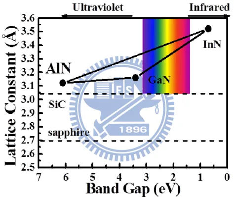
Fig. 1.1 Lattice constant as a function of bandgap energy of III-N compounds ... 5
Fig. 2.1 Schematic analogy of carriers injected into active regions and depletion through radiative, nonradiative, and leakage recombinations ... 27
Fig. 2.2 Radiative and nonradiative recombination in active region. ... 28
Fig. 2.3 (a) Cross-section schematic diagram of typical LED structures (b) Photon trajectories inside the LED ... 29
Fig. 2.4 Total internal reflect in GaN-Based LED ... 30
Fig. 2.5 The angle of total internal reflection defines the light-escape cone ... 30
Fig. 2.6 (a) Cross section TEM image of typical GaN LED structure growth on sapphire substrate. (b) Enlarge TEM image of ten pairs multiple quantum well on GaN epitaxial layer. ... 31
Fig. 2.7 Some LED light extraction schemes. ... 32
Fig. 2.8 Schematic of in-situ monitoring configuration. ... 33
Fig. 2.9 The measured reflectivity of GaN bulk layer on sapphire. ... 34
Fig. 2.10 Illustration of different polarity, (a) GaN-face (c GaN, Ga-polarity) (b) N-face (c GaN, N-polarity) ... 35
Fig. 2.11 Schematic diagrams of the cross-section GaN film viewed along the [1120] direction for N-polar GaN to explain the mechanism of the polarity selective etching. (a) Nitrogen terminated layer with one negatively charged dangling bond on each nitrogen atom; (b) adsorption of hydroxide ions; (c) formation of oxides; (d) dissolving the oxides ... 36
Fig. 2.12 Nd:YVO4 355-nm pulsed laser microPL measurement system ... 37
Fig. 2.13 (a) Knife Edge measurement diagram (b) the distance between lens and knife is 2 5μm,and laser beam spotsize is about 4.6μm ... 38
Fig. 2.14 Laser spotsize calculation and experimental results byknife edge measurement ... 39
Fig. 3.1 Schematic representation of an ALD process ... 52
Fig. 3.2 Growth procedure of AlGaN barrier and GaN well layers ... 53
Fig. 3.3 High-resolution x-ray diffraction pattern at (0002) plane for the AlGaN/GaN MQWs sample ... 54
Fig. 3.4 RSM of the sample obtained from (1015) diffraction ... 55
Fig. 3.5 Surface morphology of the grown AlGaN/GaN MQWs sample scanned by AFM ... 56
Fig. 3.6 Cross-sectional TEM image of the grown sample ... 57
Fig. 3.7 Plane-view TEM image of the AlGaN/GaN MQWs sample... 58
Fig. 3.8 Enlarged cross-sectional TEM images of the sample ... 59
Fig. 3.9 The 13K and room temperature PL spectra of the AlGaN/GaN MQWs sample. Inset shows CL image taken at E = 3.71 eV. ... 60
Fig. 3.10 The schematic diagram of the two fabricated LEDs ... 61
Fig. 3.11 L-I-V characteristics of the two fabricated LEDs ... 62
Fig. 4.1 Defect selective passivation process flow ... 73
Fig. 4.2 Top-view SEM image of the grown sample surface morphology after high temperature KOH etching process. ... 74
Fig. 4.3 Top-view SEM image of etched sample after deposit SiO2 film process. ... 75
Fig. 4.4 Top-view SEM image of etched sample with SiO2 film morphology after CMP process. ... 76
Fig. 4.5 TEM image of LED sample with defect selective passivation... 77
Fig. 4.6 SEM image of the defect passivated sample after molten KOH etching ... 78
Fig. 4.7 SEM image of the defect passivated sample after high temperature H3PO4 etching ... 79
Fig. 4.8 Cross section CL (a) and SEM image (b) of the defect passivated epi-wafer under same magnification ... 80
Fig. 4.9 L-I and V-I curve of the DP-LED and R-LED ... 81
Fig. 4.10 The reverse voltage versus current characteristics of DP-LED and R-LED 82 Fig. 5.1 Process flowchart of LED with inverted pyramid structure ... 99
Fig. 5.2 SEM image of the etched GaN surface. The inverted pyramid structures can be seen from the over etched opening holes. ... 100
Fig. 5.3 SEM cross section image of the regrown sample ... 101
Fig. 5.4 A zoom out view of the inverted pyramid structures at GaN-sapphire interface ... 102
Fig. 5.5 X-ray diffraction rocking curves for IP-LED and R-LED samples ... 103
Fig. 5.6 Surface morphology of the UVLED with inverted pyramid scanned by AFM ... 104
Fig. 5.7 The schematic of the LED with inverted micro pyramid structures ... 105 Fig. 5.8 EL spectra of IP-LED and R-LED in normal direction ... 106 Fig. 5.9 L-I-V curves of IP-LED and R-LED ... 107 Fig. 5.10 The reverse voltage versus current characteristics of IP-LED and R-LED 108 Fig. 5.11 Three-dimension far field patterns of IP-LED and R-LED ... 109 Fig. 5.12 Two-dimension far field pattern at 20 mA injection current (normal direction)
... 110
Fig. 5.13 Monte Carlo Ray tracing simulations. (a) and (b) are zoom in views at
GaN-sapphire interface for IP-LED and R-LED ... 111
Fig. 5.14 Light extraction enhancements versus different pyramid heights ... 112 Fig. 5.15 The process flowchart for fabrication of thin GaN structure ... 113 Fig. 5.16 Cross-sectional SEM images of (a) IP structure formed in the wet etching
process (b) The re-growth HIP GaN/air interface; Cross-sectional TEM images of (c) GaN-based LED structure grown on IP GaN/air template (d) The re-growth IP GaN/air boundary. The diffraction condition is g=(0002). ... 114
Fig. 5.17 Cross-sectional SEM image of the vertical LED structure after mechanical
lift-off GaN LED/Silicon from sapphire substrate. Inset shows top-view SEM image of the IP surface morphology... 115
Fig. 5.18 Surface morphology of the thin GaN LED structure after mechanical lift-off
scanned by AFM ... 116
Fig. 5.19 Room temperature Raman spectrum of GaN epilayer regrowth on IP
structure and mechanical lift-off by IP structure ... 117
Fig. 5.20 EL spectra of Ref-LED and V-LED in normal direction at 20mA. Inset
shows peak wavelength shift of Ref-LED and V-LED ... 118
Fig. 5.21 L-I-V characteristics of the two fabricated LEDs ... 119 Fig. 6.1 (a)-(d) GaN nanopillars fabrication steps ... 128 Fig. 6.2 (a) Top view SEM image of Ni nano mask, (b) Tilted SEM image of GaN
nanopillars before regrowth, (c) Top view SEM image of GaN nanopillars after regrowth, (d) Tilted SEM image of GaN nanopillars after regrowth and (e) cross section SEM image of GaN nanopillars after regrowth ... 129
Fig. 6.3 Emission spectra of optically pumped GaN nanopillars ... 130 Fig. 6.4 Peak intensity and linewidth vs. pump intensity ... 131
through recurrent scattering in GaN nanopillars ... 132
Chapter 1 Introduction
1.1 Background
Since the 1960s, many researchers studied the gallium nitride based materials and devices due to their wide direct bandgap and excellent thermal properties. However, owing the lack of GaN bulk growth methods, the GaN are often grown on foreign substrate such as sapphire or silicon carbide. It is difficult to grow high quality GaN film on these substrates for its applications to optoelectronic devices. In the 1967, the Maruska and Tietjen demonstrated the first large area single crystalline GaN thin films on sapphire substrate using chemical vapor deposition (CVD) approach [1]. In 1971, Pankove and Miller announced the first GaN blue light emitting diode at RCA laborites [2]. This device consists of an undoped n-type region, an insulating Zn-doped layer, and an indium surface metal contact [3]. However, the most of GaN based devices were still deposited on sapphire or SiC substrate using hydride vapor phase epitaxy (HVPE) system. The obstacles result from large lattice mismatch, thermal expansion coefficient mismatch and could not obtain the well conductivity at p-type GaN, which led to the GaN based LED development without eminent breakthrough. In 1986, Amano research group employed the MOCVD system to grow a thin AlN buffer layer at low temperature (LT) for decrease the dislocation density, which approach could obtain the mirror-like thin film [4]. In 1991, Nakamura used the LT GaN buffer layer could acquire the high crystal quality and mirror-like thin films as well [5]. In 1989, Akasaki (Amano et al.) was the first one used the low-energy electron-beam irradiation (LEEBI) to irradiate the suface of Mg doped gallium nitride then got p-GaN, which dopant concentration could reach to 1017 cm-3 and about 12 –cm sheet
resistance [6]. Nakamura technical group found that once the Mg doped gallium nitride under the high temperature and sufficient N2 surroundings,
then low sheet resistance p-GaN could be obtained [7]. The nitride-based compound semiconductor rapidly developed in past decade.
1.2 GaN based material and its application for light emitting
devices
GaN-based wide bandgap semiconductors are very important material system for fabrication of photon emitters in a wide range of wavelength. Therefore, wurtzitic polytypes of GaN, AlN, and InN, and their ternary and quaternary alloys have attracted a great deal of attention (LEDs) and laser diodes (LDs) [8-10]. Since wurtzite polytypes of III-nitrides form a continuous alloy system whose direct bandgap ranging from 0.7 eV for InN [11], to 3.4 eV for GaN, and to 6.2 eV for AlN [12] as shown in Fig. 1.1. In addition, the III-nitrides are superior materials for high-temperature and high-power applications. [13-15].
Nitride-based green and blue LEDs with efficiency, brightness, and longevity that are well in excess of those required for outdoor applications are already commercially available. In addition, blue LEDs are employed to pump integrated inorganic and organic media to produce colors reaching red, on the one hand, and white light on the other. In addition to the traditional displays, these LEDs have applications in traffic lights, moving signs, indicator lights, spot lights, and possibly light sources for accelerated photosynthesis, and medicine for diagnosis and treatment. Potentially, further improvement in LEDs would expand the applications to lighting with large energy savings, as LEDs are more efficient than incandescent bulbs.
1.3 An Overview of thesis
This thesis is divided into the seven parts. The first part of this thesis briefly reviews the major development of GaN light emitting devices.
In Chapter 2, we introduce the fundamental physical-mechanisms of LED science to define and judge LED performances. The current challenges for realizing the high efficiency LED are also discussed in this chapter, including reduction of dislocation density in GaN epitaxial layers and improvement of light extraction efficiency by several geometric pattern structures. We also show fabricated process systems which include metal organic chemicals vapor deposition system, chemicals wet etching process in GaN epitaxial layers and optical measurement system.
In Chapter 3, we present a novel approach of reducing propagation of threading dislocations into active region and growth of high quality AlGaN/GaN multiple quantum structure using atomic layer deposition (ALD). The crystalline quality of as-grown sample is characterized by atomic force microscope (AFM), transmission electron microscopy (TEM) and x-ray diffraction (XRD). The device performances of LED with ALD insert layer are also shown in this chapter.
In Chapter 4, we investigate the fabrication process of defect passivation LEDs (DP-LEDs). The defect selective passivation is done by using defect selective chemical etching to locate defect sites, followed by silicon oxide passivation of the etched pits, and epitaxial over growth characteristics of the DP-LEDs are shown and studied.
In Chapter 5, by combing the chemical wet etching process and lateral overgrowth methods, we fabricate the high efficiency LED with inverted pyramid (IP) structure between GaN and sapphire interface. Characteristics of the IP-LEDs are shown and studied. We also build the light prorogation modeling in IP-LED by the Monte Carlo ray tracing
methods. Then, a process technique to fabricate the vertical type LED with IP structure by mechanical lift-off and wafer bonding process are proposed and demonstrated experimentally.
In the chapter 6, we report the fabrication of GaN nanopillars and their lasing characteristics under optical pumping at room temperature. The nanopillars were fabricated from a GaN epitaxial wafer by self-assembled Ni nanomasked etching, followed by epitaxial regrowth to form crystalline facets on the etched nanopillars.
Finally, a conclusion and a brief description in the future works are presented.
References
[1] H.P. maruska and J. J. Tietjen, Appl. Phys. Lett. 15, 367 (1969)
[2] J. I. Pankove, E. A. Miller and J. E. Berleyhesier, RCA Rev. 32, 283 (1971).
[3] J.I. Pankove, E.A. Miller, D. Richman and J.E. Ber keyheiser, J. Lumin. 4, 63 (1971)
[4] H. Amano, N. Sawaki, I. Akasaki and T. Yoyoda, Appl. Phys. Lett. 48, 353 (1986).
[5] S. Nakamura, Jpn. J. Appl. Phys. 30, L1705 (1991).
[6] H. Amano, M. Kito, K. Hiramatsu and I. Akasaki, Jpn. J. Appl. Phys. 28, L2112 (1989).
[7] S. Nakamura, M. Senoh and T. Mukai, Jpn. J. Appl. Phys. 30, L1708 (1991).
[8] S. Nakamura, T. Mukai, and M. Senoh, Appl. Phys. Lett. 64, 1687 (1994).
[9] S. Nakamura, M. Senoh, N. Iwasa, and S. Nagahama, Jpn. J. Appl. Phys. 34, L797 (1995).
[10] G. Y. Xu, A. Salvador, W. Kim, Z. Fan, C. Lu, H. Tang, H. Markoc, G. Smith, M. Estes, B. Goldberg, W. Yank, and S. Krishnankutty, Appl. Phys. Lett. 71, 2154 (1997).
[11] T. Matsuoka, H. Okamoto, M. Nakao, H. Harima, and E. Kurimoto, Appl. Phys. Lett. 81, 1246 (2002).
[12] L. J. Schowalter, G. A. Slack, J. B. Whitlock, K. Morgan, S. B. Schujman, B. Raghothamachar, M. Dudley, and K. R. Evans, Phys. Stat. Sol. (c) 0, No. 7, 1997 (2003).
[13] T. G. Zhu, D. J. H. Lambert, B. S. Shelton, M. N. Wong, U. Chowdhury, H. K. Kwon, and R. D. Dupuis, Electron Lett. 36, 1971
(2000).
[14] B. S. Shelton, D. J. H. Lambert, H. J. Jang, M. M. Wong, U. Chowdhury, Z. T. Gang, H. K. Kwon, Z. Liliental-Weber, M. Benarama, M. Feng, and R. D. Dupuis, IEEE Trans Electron Devices 48, 490 (2001). [15] A. P. Zhang, J. Han, F. Ren, K. E. Waldrio, C. R. Abernathy, B. Luo, G. Dang, J. W. Johnson, K. P. Lee, and S. J. Pearton, Electronchem. Solid-State Lett. 4, G39 (2001).
Chapter 2 Mechanisms, Fabrication Process and
Measurement system
2.1 The physical mechanisms for light emitting diode
2.1.1 Internal quantum efficiency & Non-radiative recombination center
For the double heterostructure active region, the injected current provides a generation term and various radiative and nonradiative recombination processes as well as carrier leakage provides recombination term. The process of a certain steady-state carrier density in the active region could be compared to that a reservoir analogy, which is being simultaneously filled and drained, as shown in Fig. 2.1. In Fig. 2.1, there are η𝑖 = ( 𝐼
𝑒𝑉) electrons per second per unit volume being
injected into the active region. The η𝑖 , is the fraction of terminal current that generates carriers in the active region and V is the volume of the active region.
Thus, rate equation is determined as
dn
dt = 𝐺𝑔𝑒𝑛 − 𝑅𝑟𝑒𝑐 (2-1)
where Ggen is the rate of injected electrons and Rrec is the rate of
recombining electrons per unit volume in the active region. The recombination process is accompanied with spontaneous emission rate
Rsp, nonradiative recombination rate, Rnr, and carrier leakage rate, Rl, as
depicted in Fig. 2.1. Carrier leakage rate, Rl, is occurred when the
transverse or lateral potential barriers are not sufficiently high. Thus total recombination rate is expressed as below
It is common to describe the natural decay processes by a carrier lifetime, τ. In the absence of photon generation term, the rate equation for carrier decay is,
dn dt = n τ, where n τ = Rsp+ Rnr+ Rl (2-3)
The carrier rate equation in equivalent be expressed as
dn dt = Ggen − Rrec = ( I eV) − n τ (2-4)
The spontaneous photon generation rate per unit volume is exactly equal to the spontaneous electron recombination rate, Rsp, since by
definition every time an electron-hole pair recombines radiatively, a photon is generated. Under steady-state conditions (dn/dt =0), the generation rate equals the recombination rate,
(𝑒𝑉𝐼 ) =𝑛𝜏 = R𝑠𝑝+ R𝑛𝑟 + 𝑅𝑙 (2-5) The spontaneously generated optical power, Psp, is obtained by
multiplying the number of photons generated per unit time per unit volume, Rsp, by the energy per photon, hν, and the volume of the active
region V, Then
P𝑠𝑝 = hν × V × R𝑠𝑝 = 𝜂𝑖𝜂𝑟hν
𝑒 𝐼 (2-6)
where the radiative efficiency, ηr, is defined as
η𝑟 = 𝑅𝑠𝑝
R𝑠𝑝+R𝑛𝑟+𝑅𝑙 (2-7)
Usually, the ηr depends upon the carrier density and the product of ηiηr
is the internal quantum efficiency, ηint. Thus according to Eq (2-6), the
η𝑖𝑛𝑡 = 𝑃𝑠𝑝/(ℎ𝜐)
𝐼/𝑒 = 𝜂𝑖𝜂𝑟 (2-8)
Internal quantum efficiency:
𝐼𝑄𝐸 =(the number of photons emitted from active region per secend) (the number of electrons injected into LED per secend) (2-9)
Thus the internal quantum efficiency is related to ηi, the fraction of
terminal current that generates carriers in the active region, and to ηr, the
fraction of rates between radiative recombination to total carriers’ recombination. According to Eq (2-8), we can enhance the internal quantum efficiency of LEDs by either increasing radiative recombination rate, Rsp, or decreasing nonradiative recombination rate, Rnr, and carrier
leakage rate, Rl.
The possible recombinative paths of injected electrons and holes are shown in Fig. 2.2. Typically, material defects —including defects that extend over some distance of the material such as threading dislocations and more localized point defects such as vacancies and impurities — act as centers of nonradiative recombination. Thus the overall goal in this stage is to enhance the radiative recombination rate and suppress the nonradiative recombination rate. Therefore, significantly improvements of grown-layers quality associating with appropriate design of LEDs structures is the main thought to improve the internal quantum efficiency. 2.1.2 The limits of light extraction efficiency
A cross-section schematic diagram of typical LED structures is shown in Fig. 2.3 (a). The most serious problem with rectangular cubic may be that the photons generated at a point in the active region will be
trapped inside the GaN and sapphire region as shown in Fig. 2.3 (b), due to thecontinued total internal reflections off the chip wall as illustrated in Fig. 2.4. Assume that the angle of incidence in the semiconductor at the semiconductor- air interface is given by θ1. Then the angle of incidence of
the refracted ray, θ2, can be derived from Snell’s law
𝑛𝑠sin 𝜃1 = 𝑛𝑎sin 𝜃2 (2-10) Where, ns and na are the refractive indices of semiconductor and air,
respectively. The critical angle θc for total internal reflection is obtained
using θ2 = 90°, using Snell’s law, one obtains.
sin 𝜃𝑐 = (𝑛𝑎
𝑛𝑠) sin 90
0, 𝜃
𝑐 = sin−1(𝑛𝑛𝑎
𝑠) (2-11)
The angle of total internal reflection defines the light-escape cone as shown in Fig 2.5. Light emitted into the cone can escape from the semiconductor, whereas light emitted outside the cone is suffered from the total internal reflection. The surface area of the escape cone is given by the integral
Area = ∫ 𝑑𝐴 = ∫𝜃𝑐 2
𝜃=0 πr sin 𝜃𝑟dθ = 2πr2(1 − cos 𝜃𝑐) (2-12)
Assume that light is emitted from a point-like source in the semiconductor with a total power of Psource. Then the power that can
escape from the semiconductor is given by
P𝑒𝑠𝑐𝑎𝑝𝑒 = Psource2𝜋𝑟2(1−cos 𝜃𝑐)
4𝜋𝑟2 (2-13)
Where 4πr2 is the entire surface area of the sphere with radius r. The calculation indicates that only a fraction of the light emitted inside a semiconductor can escape from the semiconductor. This fraction is given by
η𝑒𝑥𝑡 = P𝑒𝑠𝑐𝑎𝑝𝑒
Psource =
2𝜋𝑟2(1−cos 𝜃 𝑐)
4𝜋𝑟2 (2-14)
Expanding Eq (2-14) into power series and neglecting higher than second-order terms yields
η𝑒𝑥𝑡 = 12*1 − (1 −𝜃𝑐2 2 )+ = 1 4𝜃𝑐 2 ≈1 4 𝑛𝑎 𝑛𝑠 , 𝑛𝑎 = 1, 𝑛𝑠 = 𝑛𝐺𝑎𝑁 = 2.45 (2-15)
According to Eq (2-15), only a few percent (~4%) of the light generated in the semiconductor can escape from a planar LED.
2.2 Key issues for realizing high efficiency LEDs 2.2.1 Quality issues of GaN epitaxial layers
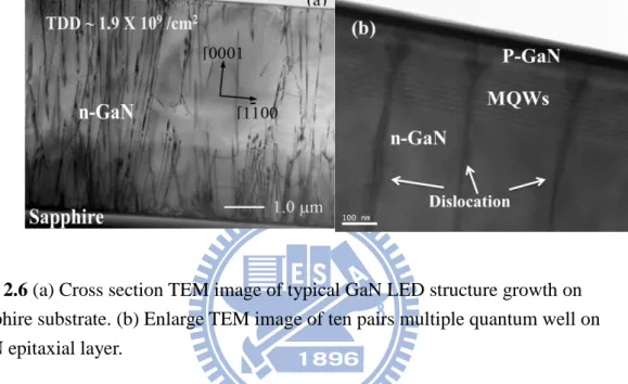
The GaN-Based material and devices are often epitaxially grown on foreign substrates, such as silicon carbon (SiC) or sapphire. These substrates must be used because wafers of GaN are not available as in the case of more common semiconductors. A layer grown at lower temperature, the nucleation layer, is used to initiate oriented growth on the substrate, followed by epitaxial growth on this layer at higher temperatures. The as grown GaN epitaxial layer has high threading dislocation density (TDD) typically in the range of 108-10 cm-2 due to the mismatches in lattice constants (16%) and thermal expansion coefficients (39%) between GaN and sapphire, resulting in defect-mediated nonradiative recombination of electron-hole pairs and reduced mobility because of carriers trapped by defect centers. Fig. 2.6 (a) shows the cross section TEM image of typical GaN LED structure growth on sapphire substrate, the threading dislocation location density is higher than 109 cm-2 in GaN epitaxial layers and some threading dislocations propagate
through the active region of LED, as shown in Fig 2.6 (b). These threading densities need to be drastically reduced because dislocations quench light emission of LEDs. These dislocation defects can be reduced by substrate patterning techniques such as Epitaxial Lateral Overgrowth (ELOG) [1], or pattern sapphire substrate [2]; above approaches rely on spatial filtering, terminating, and turning of threading dislocations, so they do not reach the device active region. In the chapter 3 and 4 of this thesis, we report novel epitaxial approach and defect passivation structure to effectively block thread dislocation from the substrate to active region. In particular, defect passivation structure not only block the propagation of TD but also can act as light scattering sites to improve LED light extraction efficiency, similar to the use of patterned GaN-sapphire interface to reduce light trapped by total internal reflection.
2.2.2 Light extraction of GaN LEDs
Limitations in light extraction include total internal reflection at interfaces and light absorption within the device or in the packaging. The generation of light in active region of an LED is mostly captured with GaN and sapphire by the guided modes. It is due to the high contrast refractive index at the GaN (n=2.45)/air (n=1) and GaN/sapphire (n=1.78) interfaces, resulting in total internal reflection that traps light in the high index GaN and in the sapphire substrate. Some light-extraction methods are shown in Fig. 2.7 and discussed in following.
(a) Patterned sapphire substrate: Patterned sapphire substrate with chemical wet etching in between epitaxial growth steps has provided another way to improve light extraction efficiency. The light with large incident angle will be reflected coupling into escaping cone. However, some light still might travel multi-times and absorbed finally.
Photonic crystals can be used in multiple ways to increase light extraction efficiency. Two-dimensional (2D) photonic crystals can be used to scatter waveguided modes out of the active layer region. Another approach is to use 2D photonic crystals to change the photonic density of states in the active layer so that no in-plane modes are permitted [3]. This would cause all emitted light from the quantum wells to be normal to the LED surface so that it would lie within the escape cone and not be reflected. A third possibility is to increase the internal quantum efficiency by enhancing the photonic density of states at the LED emission wavelength. These fabrication processes often involves micro lithography and etching.
In the chapter 5 of this thesis, we report high extraction efficiency LED with inverted pyramid structure at the GaN-sapphire interface without complex lithography process. Form Monte Carlo simulation and experiment results, the IP structure can efficiently redirect the propagation of the laterally guided modes to the surface normal direction. The proposed method not only can improve the light extraction efficiency but also provide a sacrificial layer for substrate lift-off technique.
2.3 Metal Organic Chemical Vapor Deposition System
For the past twenty years, metal organic chemical vapor deposition (MOCVD) systemhas become a commonly used technology for production of III-V compound semiconductor optoelectronic and electronic devices. The term ―MOCVD‖ was originated by Manasevit [4-6], and it was used to express a form of chemical vapor deposition (CVD) utilizing the new process transported metals using organic compounds for one or more of the precursors. Alternative names included OM (OrganoMetallic) CVD, MOVPE (Vapor Phase Epitaxy), and OMVPE are all the same meaning, except epitaxy is a special case of thin
film deposition where the layer replicates the crystal structure of the substrate. Because of the improvement in the material quality produced by MOCVD, many important III-V devices have become commercially viable. Indeed, the achievement of growing ultra-bright blue light emitting diodes by MOCVD [7] makes this technology be a leading candidate for manufacturing optoelectronics devices. In this dissertation, we use MOCVD system to grow all the epitaxial structures. The detailed descriptions and specific functions of MOCVD system are given in this chapter.
2.3.1 Reaction Equations
The MOCVD process for the growth of compound semiconductor materials and devices originated in the pioneering work has been done by H. M. Manasevit. Briefly, MOCVD process relies on vapor transport of the group III alkyls combined with group V hydrides into heated substrate. At the heated substrate, the molecules pyrolyze to produce the group III and group V elements needed for formation of desired III-V semiconductors and subsequent reaction. The simplest case in MOCVD [8] involves a pyrolysis reaction of the vapor of a volatile organometallic compound and a gaseous hydride, given by:
𝑅𝑛𝐴 + 𝐷𝐻𝑛 → 𝐴𝐷 + 𝑛𝑅𝐻 (2-16) A and D are the constituent species for the deposited solid. R is an organic radical ofsome unspecified form, and many organometallic compounds have been studied as sources for the MOCVD processes. However, the lower order organic radicals are generally used, such as a methyl- or ethyl-radical, and the most important are trimethylgallium (TMGa), triethylgallium (TEGa), trimethylaluminum (TMAl), and trimethylindium (TMIn). Desirable properties include a reasonable vapor pressure at room temperature or below, high purity, low cost, a low
affinity for oxygen and water vapor, and low toxicity. Unfortunately, many of the MOs that meet the vapor pressure and purity needs best are also highly reactive with oxygen. They are therefore contained in stainless steel bubblers, and great effort is made to avoid their contamination by air. Contrasting with V sources, metalorganic group III source are either liquids, such as TMGa, TEGa, and TMAl, or solids such as TMIn. Therefore, the organmetallic constituents generally are transported to a heated substrate by passing a carrier gas, over or through the compound contained in a constant-temperature bubble vessel. Highly purified hydrogen or nitrogen is bubbled through the liquid to transport the material into the reactor. Knowledge of the vapor pressure (at the bubble temperature and pressure) and the carrier gas flow rate is sufficient to determine the transport rate. On the other hand, most MOCVD growth of III-V compound semiconductors and alloys involves the use of hydrides, such as arsine, phosphine, or ammonia for the column V species. In principle, these are the simplest of column V sources to use because they are already gaseous and supplied from simple cylinder-based delivery system. In spite of the fact that they are extremely toxic, since they are relatively inexpensive with high purity layers. The dopants processes are available in the form of MOs in bubblers (for example, Cp2Mg), or in the form of gases (for example, SiH4). Because of the concentration may be varied over a wide range, the dopant sources have to adjust the concentration, typically with a dilution network. The growth of semiconductor alloys by MOCVD is easily accomplished by mixing the vapors from the different alloy constituents in the appropriate vapor phase ratio to form the desired composition. A general equation for a ternary alloy is given by:
For GaN-based material growth, the first MOCVD system design for GaN growth was developed by Maruska and Tietjen [10]. Soon after, Manasevit applied this technique to grow GaN onto sapphire substrate [11]. The choice of sapphire substrate results from the facts that no GaN bulk substrate are available and a very stable material is required to deal with the high temperature required for GaN growth at around 1000oC. Based on the equation (2-16), the GaN epitaxy process by using MOCVD can bewritten:
(CH3)3𝐺𝑎(𝜈) + 𝑁𝐻3(𝜈) → 𝐺𝑎𝑁(𝑠) + 3𝐶𝐻4(𝜈) (2-18) which v is vapor and s is solid. This simple equation, however, ignores the complicated reaction path and reactive species in the reactor. The incoming materials partially decompose and are then adsorbed on the surface. Then, they decompose further or aredesorbed. The atoms and radicals move around on the surface with growth occurring at steps for smooth, two-dimensional layers, replicating the structure of the substrate [12]. In fact, the detail of the reaction is still unknown. Nishizawa, Abe and Kurabayashi (1985); Denbaars et al. (1996) [13] reported a reaction pathway arise form growing GaAs epitaxial layers involves homogenerous decomposition of TMGa :
𝐺𝑎(CH3)3(𝜈) → 𝐺𝑎(CH3)2(𝜈) + 𝐶𝐻3(𝜈) (2-19) 𝐺𝑎(CH3)2(𝜈) → Ga(CH3)(𝜈) + 𝐶𝐻3(𝜈) (2-20) Ga(CH3)(𝜈) → Ga(𝜈) + 𝐶𝐻3(𝜈) (2-21) In the other hand, the group V source, NH3, is considered to decompose heterogeneously on the GaN surface or reactor wall to provide atomic nitrogen, or a nitrogen containing radical at high grow temperature.
𝑁𝐻3(𝑠/𝜈) → 𝑁𝐻3−𝑥(𝑠/𝜈) + 𝑥𝐻(𝑠/𝜈) (2-22) Combine the above mentioned equation, one possible growth mechanism
of GaN that occur at the solid/vapor interface could be expressed as follows:
Ga(𝐶𝐻3)(𝑠/𝜈) + 𝑁𝐻(𝑠/𝜈) → 𝐺𝑎𝑁(𝑠) + 1
2𝐻(𝜈)+ 𝐶𝐻3 (2-23)
Although the growth mechanism of GaN can be briefly expressed by Eq. (2-23). The most difficult topic is the kinetics of the process and growth mechanism occurring at solid/vapor interface during MOCVD growth.
Optimization of MOCVD grown condition is typically done by empirical studies of external parameters such as grown temperature, V/III ratio, and mass flow rate. These studies have identified three regions of growth: mass transport limited, desorption and surface kinetically limited regimes. Conventional GaN MOCVD growth is usually performed in mass transport limited regime that takes place over a wide temperature (600~1100oC), and the growth is limited by mass transport of the column III reactant to the growing interface.
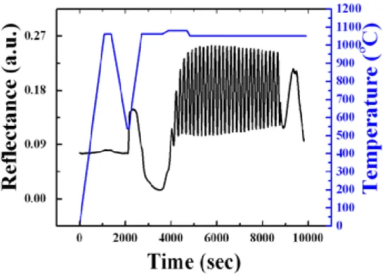
2.3.2 In-Situ Reflectance Monitoring During III-Nitrides Growth For many years, high vacuum growth techniques such as MBE have enjoyed the advantage of using in situ diagnostic tools such as RHEED to determine substrate surface conditions and measure growth rates. Now MOCVD has responded with a variety of optical techniques to perform diagnostic on the layers as they grow [14]. Indeed, the in-situ monitoring of optical techniques is very useful for growing optoelectronic devices such as VCSELs due to the stringent requirement of phase matching. The in-situ monitoring is also an important tool to grow III-Nitride materials on foreign substrate, such as sapphire, because the limitation of homoepitaxial substrate absence is usually overcome by growing a low-temperature (LT) AlN [15] or GaN [16] nucleation layer on a sapphire substrate before the high-temperature (HT) growth. In order to
realize the growth information during growing GaN, the in-situ monitoring tool is usually used to extracting growth information. In our D-75 system, we use an in-situ normal incidence reflectance method to extract the information of growth rate and crystal quality. The tungsten-lamp reflectometry is applied as the in-situ monitoring in D-75 type MOCVD system. The schematic of the configuration is shown in Fig. 2.8. Two optical heads are mounted on the top flow flange of the reactor and monitoring the growth conditions for the upper and lower points of the wafer surface. An optical head couples two fibers; one is from the light source with the continue band wavelength, and the other is to the detector. Suppose the optic index of thin film materials is different from the substrate, the reflectance and interference from the underlying interface can be described as R = |r|2 , and r can be described as [17]
r(𝑡) = 𝑟∞+𝑟𝑖𝑒𝑥𝑝(−𝑖4𝜋𝛽2)
1+𝑟∞𝑟𝑖𝑒𝑥𝑝(−4𝜋𝛽2) (2-24)
where β2 = 4πnd/λ is the phase shift in the film, 𝑟∞ and 𝑟𝑖 are the
reflectance of an infinitely thick film of the top layer and the internal layer reflectance, respectively.
The 𝑒𝑥𝑝(−𝑖4𝜋𝛽2)term describe and oscillatory behavior of β2. Thus growth rate can be determined with the refractive index at certain growth temperature at a given wavelength. The growth rate can be obtained by
G𝑅 = 𝜆𝑇𝑑/2𝑛𝜆 (2-25) where 𝜆 is the chosen wavelength, Td is the oscillation period of the reflectivity curve, 𝑛𝜆 is the refractive index of the epitaxial layer at the growth temperature for 𝜆 This is very useful controlling the thickness of the LT nucleation layer. Fig. 2.9 shows the example for the measured reflectivity of a GaN bulk structure. Furthermore, applying the in-situ monitoring system, we can also do temperature calibrations. In the former case, one can perform temperature calibration with eutectic wafers
(Al-coated Si wafers or Silver-coated Si wafers) quickly and easily by plotting the reflectance as a function of temperature, while the temperature of the reactor is ramped slowly. As the temperature ramping up to the melting point of aluminum or silver, 660oC, and 961oC, respectively, the reflectance would be drop down rapidly. Thus one could know the meter temperature is the metal melting point. In the latter case, one can design a ―calibration‖ structure that contains layers of different compositions or different growth condition in a single growth run without requiring any post growth characterization.
2.4 Etching process in molten KOH
The discrepancy of etching characteristics in Ga-face (c GaN,
Ga-polarity) and N-face (c GaN, N-polarity) has been specifically
investigated as illustrated in Fig. 2.10. Some reports showed that gallium nitride could be etched in the aqueous sodium hydroxide (NaOH) solution but etching ceased when the formation of an insoluble coating of presumably gallium hydroxide (Ga(OH)3) [18, 19]. For further etching, it
would need removing of the coating by continual jet action. All other various aqueous acid and base solutions have been tested for etching of GaN at temperature up to 75oC were listed in Table 2.1 [20-22]. The undetermined etch rate (nm/min) was because it various from sample to sample and differences in the defect density. According to the research reports in recent years; the common cognition related to gallium nitride etching process was that the most of gallium nitride could be etched rapidly in N-face. The reason for the face-dependent gallium nitride etching process has been studied by Li et al., who utilized the X-ray photoelectron spectroscopy (XPS) to examine the surface chemistries before and after etching process in aqueous KOH solutions for both Ga- and N-face gallium nitrides. The conclusion is that the different etching
results in Ga- and N-face gallium nitride crystals are due to the different states of surface bonding. Besides, the most important is the etching process only dependent on the polarities, not on the surface morphology, growth condition and which atoms form the surface termination layer. The GaN chemical etching reaction with KOH could be described as the following formula [23]: 3 3 2 KOH 2O Ga O 2NH 3H 2GaN (2-11)
Here, the molten KOH act as a catalyst and a solvent for the resulting Ga2O3 (Fig. 2.11 (d)) as well. The mechanism about etching N-face
gallium nitride substrate was illustrated in Fig. 2.11 The hydroxide ions (OH) were first adsorbed on the gallium nitride surface (Fig. 2.11 (b))
and finally react with Ga atoms once the OH ions with sufficient
kinetic energy as shown in the Fig. 2.11 (c). The etching could be started at step (c) if the surface was Ga-terminated. The inertness of Ga-face GaN was ascribed to the hydroxide ions would be repelled by the negatively-charged triple dangling bonds of nitrogen near the surface. Thus, if the Ga-face GaN was Ga-terminated, the etching process stops after the first gallium atom layer was removed. In contrast, the N-face GaN, every nitrogen atom with single dangling bond to prevent the hydroxide ions attacking from Ga atoms.
2.5 Micro photoluminescence spectroscopy (μ-PL)
Photoluminescence (PL) spectroscopy has been used as a measurement method to detect the optical properties of the materials because of its nondestructive characteristics. PL is the emission of light from a material under optical excitation. Reducing the laser beam spotsize to micrometer by beam expanders and objective lens is the so-called μ-PL. The laser light source used to excite carriers should have larger energy band gap than the semiconductors. When the laser light is
absorbed within the semiconductors, it would excite the carriers from the valence band to the conduction band. Then, it produces the electrons in the conduction band and the holes in the valence band. When the electron in an excited state return to the initial state, it will emit a photon whose energy is equal to the energy difference between the excited state and the initial state, therefore, we can observed the emission peak from PL spectrum. The schematic setup of our μ-PL system is shown in Fig. 2.12 The pumping source is Nd:YAG 355 pulsed laser with a pulse width of ~1nsec at a repetition rate of 1KHz.The PL is collected by a 15X objective lens and straightly collected by spectrometer with a charge-coupled device (Jobin-Yvon IHR320 Spectrometer) or collected by a fiber with 200μm core, which rotating in the normal plane of the sample, and also coupled into spectrometer. The spectral resolution is about 0.1 nm for spectral output measurement. We can also monitor the image and spatial distribution on the sample surface by charge-coupled device (CCD) and beam view, respectively.
2.5.1 Pumping power density and spotsize calculation
The optical pumping of the samples was performed using frequency-tripled Nd:YVO4 355-nm pulsed laser with a pulse width of 1ns at a repetition rate of 1 kHz. The microPL measurement system was shown in Fig 2.12 It is often necessary to calculate the power density (Power/Area) of a laser beam (for example, when trying to determine whether a beam will damage an optic or detector).Power density is expressed in watts per square meter (W/m2) or milliwatts per square centimeter (mW/cm2). Usually power density is more often expressed in terms of W/cm2 when making surveys. In our experiments, the pumping power density can be presented by following equation
(2-26) where Paverage is the laser optic power measured by power detector, 0.3 is
the value of calibration when passing through the 15X objective lens. And,α (=0.85) is the absorption coefficient of the GaN, R is the radius of the laser beam in centimeters.M2(=1.3) is defined as the ratio of the waist-diameter-divergence product, 2Wm‧2θm (usually measured in units
of mm‧rad),to that expected for a Gaussian beam. Specification of laser shows the full angle is 3mrad,beam waist location is -135mm and M2 is 1.3, so that initially spotsize which is 75.37μm can be obtained by using equation 2-27
0 (2-27) The distance between laser and objective lens is about 121.7cm, according to equation 2-26 and 2-27, spotsize expands to 1.83mm , then be focused to 0.8μm by a 15X objective lens which focal length was 13mm by using equation 2-27 2 0 0 Z (2-28) 2 0 0 1 1 Z Z (2-29) 1 2 f (2-30) In other words, the theoretical model of laser beam spotsize calculation results indicated that the value of beam radius is 0.8μm, Rayleigh range is 5.73μm and the diverge half-angle is 0.14 rad after going through 15X objective lens.
In order to know the real beam raidus, we use Knife Edge experiment
2 2 ) ( 3 . 0 sec 1 sec 1 P Density Power R M n m average
to measure Nd:YVO4 355nm pulsed laser. Under a fixed excited power, we can get the relationship of normalized intensity vs. distance that the knife moved, as shown in Fig. 2.13(a). The distance between 10% and 90% of full scale needs to multiple a factors of 0.78125, and the value is the called pumping spotsize. We have presented some knife edge results obtained on measurements of various Z axis value. For example, when moving knife away from the objective lens focal point about Z=25μm, the spotsize will be attained 4.6um as shown in Fig. 2.13(b). Vary objective lens distance Z from -125μm to 325μm, then we can obtained Gaussian beam curves of the laser, and its diverge half-angle is 0.147 rad. The calculation of Nd:YVO4 pulsed laser beam spotsize is very similar to our experimental results. The comparison between calculation results and experimental results as shown in Fig. 2.14 and Table 2.2
Etching solutions GaN etch temperature Citric acid 75C Succinic acid 75C Oxalic acids 75C Nitric acid 85C Phosphoric acid 82C Hydrochloric acid 80C Sulfuric acid 82C Potassium triphosphate 75C
Nitric acid/potassium triphosphate 75C
Hydrochloric acid/potassium triphosphate 75C
Boric acid 75C
Nitric/boric acid 75C
Potassium tetra borate 75C
Sodium tetra borate 75C
Potassium triphosphate 75C
Fig. 2.1 Schematic analogy of carriers injected into active regions and depletion
Fig. 2.3 (a) Cross-section schematic diagram of typical LED structures (b) Photon
Fig. 2.4 Total internal reflect in GaN-Based LED
Fig. 2.6 (a) Cross section TEM image of typical GaN LED structure growth on
sapphire substrate. (b) Enlarge TEM image of ten pairs multiple quantum well on GaN epitaxial layer.
Fig. 2.10 Illustration of different polarity, (a) GaN-face (c GaN, Ga-polarity) (b) N-face (c GaN, N-polarity)
Fig. 2.11 Schematic diagrams of the cross-section GaN film viewed along the [1120]
direction for N-polar GaN to explain the mechanism of the polarity selective etching. (a) Nitrogen terminated layer with one negatively charged dangling bond on each nitrogen atom; (b) adsorption of hydroxide ions; (c) formation of oxides; (d) dissolving the oxides
Fig. 2.13 (a) Knife Edge measurement diagram (b) the distance between lens and
Fig. 2.14 Laser spotsize calculation and experimental results byknife edge
References
[1] A. Usui, H. Sunakawa, A. Sakai and A. A. Yamaguchi, Jpn. J. Appl. Phys. 36, L889 (1997).
[2] M. Yamada, T. Mitani, Y, Narukawa, S. Shioji, I. Niki, S. Sonobe, K. Deguchi, M. Sano and T. Mukai, Jpn. J. Appl. Phys. 41, L1431 (2002). [3] Kenji ORITA, Satoshi TAMURA, Toshiyuki TAKIZAWA, Tetsuzo UEDA, Masaaki YURI, Shinichi TAKIGAWA and Daisuke UEDA Jpn. J. Appl. Phys. 43,5809-5813(2004)
[4] J. B. Mullin, S. J. C. Irvine, and J. Tunnicliffe, J. Cryst. Growth, 68, 214, (1984)
[5] B. Cockayne, and P. J. Wright, J. Cryst. Growth, 68, 223, (1984) [6] H. M. Manasevit, Appl. Phys. Lett. 12, 156, (1968)
[7] S. Nakamura, T. Muksi, and M. Senoh, Appl. Phys. Lett. 64, 1687, (1994)
[8] H. M. Manasevit, and W. I. Simpson, J. Electrochem. Soc, 116, 1725, (1969)
[9] Alan G. Thompson, Materials Letters, 30, 255, (1997)
[10] H. P. Maruska, and J. J. Tietjen, Appl. Phys. Lett., 15, 367, (1969) [11] H. M. Manasevit, F. Erdmann and W. Simpson, J. Electrochem. Soc, 118, 1864, (1971)
[12] S.Yu. Karpov, V.G. Prokofjev, E.V. Yakovlev, R.A. Talalaev, Yu.N. Makarov, MRS J.Nitride Semicond. Res. 4, 4, (1999)
[13] S. P. DenBaar, B. Y. Maa, P. D. Dapkus, and H. C. Lee, J. Cryst. Growth, 77, 188, 1986[14] D. E. Aspnes, IEEE J. Select. Topic Quant Elect., 1, 1054, (1995)
[15] H. Amano, N. Sawaki, I. Akasaki, and Y. Toyoda, Appl. Phys. Lett., 48, 353, (1986)
[16] S. Nakamura, Jpn. J. Appl. Phys., 30, L1705, (1991)
[17] W. G. Breiland, and K. P. Klleen, J. Appl. Phys., 78, 6726, (1995) [18] T.L. Chu, J. Electrochem. Soc. 118, 1200 (1971).
[19] J.I. Pankove, J. Electrochem. Soc. 119, 1118 (1972).
[20]H. Cho, D.C. Hays, C.B. Vartuli, S.J. Pearton, C.R. Abernathy, J.D. MacKenzie, F. Ren, J.C. Zolper, Mater. Res. Soc. Symp. Proc. 483, 265 (1998).
[21] C.B. Vartuli, S.J. Pearton, C.R. Abernathy, J.D. MacKenzie, F. Ren, J.C. Zolper, R.J. Shul, Solid-State Electron. 41 (12), 1947 (1998).
[22] S.J. Pearton, R.J. Shul, Gallium nitride I, in: J. Pankove, T.D. Moustakas (Eds.), Semiconductor and Semimetals Series, vol. 50, Academic Press, New York, NY, p. 103 (1998).
[23] D. Li, M. Sumiya, S. Fuke, D. Yang, D. Que, Y. Suzuki, Y. Fukuda, J. Appl. Phys. 90, 4219 (2001).
Chapter 3 Growth and fabrication of high quality
atomic layer deposition GaN light emitting devices
3.1 The progress of AlGaN/GaN Multiple Quantum Well
The AlGaN/GaN multiple quantum wells (MQWs) have attracted much attention because of their unique properties, such as a high conduction band offset, better carrier confinement, large longitudinal (LO) phonon energy, and ultra-fast carrier and intersubband relaxation, making AlGaN/GaN MQWs promising structures for realizing ultraviolet (UV) light emitting diodes (LEDs), and laser diodes (LDs) [1-5]. Recent reports indicated that the optical and electrical properties of AlGaN/GaN MQWs were very sensitive to the crystalline quality and the threading dislocation density (TDD) in the AlGaN/GaN epilayer [6, 7]. So far most AlGaN/GaN MQWs structures were grown on lattice-mismatched foreign substrates such as sapphire, making it difficult to grow device-quality MQWs due to the lattice mismatch and the misfit in the thermal expansion coefficients between these two material systems. Recently high quality AlGaN/GaN heterostructures using quasi AlGaN formed by AlN/GaN superlattices as barrier layers was reported [8, 9]. However, these results mainly focused on the electrical properties used for AlGaN/GaN high electron mobility transistors and no optical properties were reported. In this paper, we report the growth of low dislocation density and crack-free AlGaN/GaN MQWs by using the atomic layer deposition (ALD) grown AlN/GaN superlattices (SLs) as the AlGaN barrier. The as-grown AlGaN/GaN MQWs sample had low defect density, smooth surface morphology with small root-mean-square (RMS) roughness value, and sharp interfaces. In addition, the AlGaN/GaN MQWs sample showed a sharp photoluminescence (PL) spectrum and a
uniform cathodoluminescence (CL) pattern.
3.2 The principle of Atomic Layer Deposition
Atomic Layer Deposition (ALD) is a chemical vapor deposition (CVD) technique, which is capable of processing extremely conformal, highly uniform and high quality thin films with really low amount of defects. A large number of standard materials are available for deposition in table 1[10]. The principle of ALD is based on sequential pulsing of special precursor vapors, each of which forms about one atomic layer each pulse. Since each pair of gas pulses (one cycle) produces exactly one monolayer of film, the thickness of the resulting film may be precisely controlled by the number of deposition cycles. Normally an ALD growth cycle consist four steps Fig. 3.1 (a) Exposure of the first precursor A, (b) purge of the chamber, (c) exposure of the second precursor B, and (d) further pure of the chamber. This growth cycle is repeated as long as desired film thickness is reached. The deposition may be defined as self-limiting since one, and only one, monolayer of the reactant species remains on the surface after each exposure. In this case, one complete cycle results in the deposition of one monolayer of the compound on the substrate. Repeating this cycle leads to a controlled layer-by-layer growth. Thus the film thickness is controlled by the number of precursor cycles rather than the deposition time, as is the case for a CVD processes. This self-limiting behavior is the fundamental aspect of ALD and understanding the underlying mechanism is necessary for the future exploitation of ALD.
3.3 The Fabrication of ALD AlGaN/GaN MQWs
The AlGaN/GaN MQW structures were grown by the low-pressure metal-organic chemical vapor deposition VEECO D75 system. The TMGa, TMAl and gaseous NH3 were employed as the reactant sources
for Ga, Al and N, respectively and H2 and N2 were used as the carrier
gaseous. The (0001)-oriented sapphire substrate with a 0.2 offset was first heated to 1000C under an H2 ambient for 5 min. Then, a 2-m-thick
GaN epilayer was grown after the deposition of a low-temperature nucleation layer. Finally, the AlGaN/GaN MQWs structure comprising three GaN wells and four AlGaN barriers were grown at 850C in H2+N2
atmosphere. Particularly, the AlGaN barriers were grown using the ALD technique. The ALD process involves alternate control of mass flow of TMAl and TMGa gas during the growth of AlGaN barrier to form six pairs of AlN/GaN SLs. Fig. 3.2 shows the growth procedure of the AlGaN barrier and GaN well layer. The TMAl and TMGa flow time of AlN and GaN layer were 6.8 and 19.8sec, respectively under a continuous flow of the NH3 gas at 850°C. The growth rate of the ALD grown AlGaN
barrier measured by an in-situ Filmetrics optical monitoring system was about 0.14µm/hr. After the AlGaN barrier was grown, only TMGa was introduced into the reactor for 34.8second to grow the GaN well.
3.4 Characteristic of AlGaN/GaN MQWs with ALD grown
AlGaN Barriers
The surface morphology of the as-grown sample was observed by atomic force microscope (AFM) with a scanning area of 5 μm 5 μm. Crystalline quality was evaluated by high resolution X-ray diffraction (HRXRD) and reciprocal space mapping (RSM), and Cu K radiation
![Fig. 2.11 Schematic diagrams of the cross-section GaN film viewed along the [ 1 1 20 ] direction for N-polar GaN to explain the mechanism of the polarity selective etching](https://thumb-ap.123doks.com/thumbv2/9libinfo/8477979.183876/52.892.189.655.265.838/schematic-diagrams-direction-explain-mechanism-polarity-selective-etching.webp)