行政院國家科學委員會專題研究計畫 期中進度報告
一維氧化鋅奈米結構的摻雜效應與光電特性研究(1/3)
計畫類別: 整合型計畫 計畫編號: NSC94-2216-E-009-025- 執行期間: 94 年 08 月 01 日至 95 年 07 月 31 日 執行單位: 國立交通大學材料科學與工程學系(所) 計畫主持人: 陳三元 報告類型: 精簡報告 處理方式: 本計畫可公開查詢中 華 民 國 95 年 5 月 27 日
一維氧化鋅奈米結構的摻雜效應與光電特性研究(1/3)
氧化鎂
摻雜
氧化鋅奈米柱之
低溫製程與熱處理對於其結構與光電性質研究Low-temperature process and effect of thermal annealing on structural and
optical properties of MgO-coated ZnO nanorods
計畫編號:NSC94-2216-E-009-025 -執行時間:94/08/01 ~ 95/07/31 主持人:陳三元 教授 交通大學材料科學與工程學系 中文摘要 本研究利用化學溶液法在低溫環境中在氧化鋅薄膜的矽基板上,製備出規則排列氧 化鎂摻雜的氧化鋅奈米柱,並分析氧化鋅奈米柱和氧化鎂包覆氧化鋅奈米柱後經熱處理 後之結構及光學特性。氧化鋅奈米柱經過後熱處理均可大幅增加光學品質,且在高溫下 氧化鋅奈米柱的晶體結構也有明顯改變。氧化鎂包覆氧化鋅奈米柱後經熱處理後在化學 特性分析中可以看出,鎂原子可以由氧化鋅奈米柱的缺陷路徑成功的擴散至奈米結構 中,並且與鋅及氧元素產生化學鍵結反應。而在光學特性的研究上,氧化鋅奈米柱經過 熱處理可改變可見光放射位置和強度,而且發現在紫外光放射有藍位現象,也證明鎂原 子擴散至奈米結構,形成氧化鎂摻雜的氧化鋅奈米柱。經由本研究的結果顯示,我們可 以利用常溫的水溶液合成法結合熱處理可以製備出規則排列氧化鎂摻雜的氧化鋅奈米 柱。 關鍵字: 陣列化 ZnO 奈米柱、氧化鎂包覆、熱處理、光電特性、微觀結構 Abstract
The effect of thermal annealing on the structural and optical properties of MgO-coated ZnO nanorods structures prepared by solution techniques were investigated with scanning electron microscopy (SEM), X-ray diffraction (XRD), and photoluminescence (PL) measurements. After thermal annealing process, Mg-doped ZnO nanorods have been grown on on silicon substrates buffered with ZnO film. Structural analyses indicate that the nanorods grown on Si substrates are oriented in the c-axis direction and the nanorod possesses the single-crystalline hexagonal structure. No phase separation is observed when the annealing temperature increased to 900 oC. The MgO-coating ZnO nanorods annealed at above 800 oC showed the alloy formation due to diffusion of the Mg atoms into the ZnO nanorods. PL spectra displayed a blue shift of the near-band-edge emission, indicative of an increase in the band gap of the Zn1-xMgxO alloy.
Keywords: Allayed ZnO nanorods;MgO-coated ;Optoelectronic properties ;Thermal
I. Introduction
ZnO has a wide band gap of 3.3 eV at room temperature, making it highly promising for great potential applications in manufacturing electronic and optoelectronic devices, especially ultraviolet (UV) laser devices [1].Recent investigations have demonstrated that directionally grown ZnO nanorods can effectively reduce the threshold power, achieving UV lasing emission at room-temperature [2]. The photoluminescence (PL) spectra of ZnO typically exhibit UV and visible PL peaks. It is well-known that chemical doping, as well as intrinsic lattice defects, greatly influences electronic and optical properties of ZnO. Doped ZnO are of technological importance because of their great potential for applications to transparent conducting electrodes (doping group III B elements or fluorine) [3,4] and insulating or ferroelectric layers (doping Li or Mg)[5] in optoelectronic devices. Alloying ZnO phase with MgO or CdO has been investigated for widening the bandgap of the ZnO based materials [6]. According to the phase diagram of ZnO/MgO binary systems [7], the thermodynamic solid solubility of MgO in a ZnO matrix is less than 4 mol%. However, since the ionic radius of Mg2+ (0.57 Å) is almost the same as that of Zn2+ (0.60 Å ) [8], Zn2+ can be replaced by Mg2+ in the ZnO matrix. Furthermore, it is well known that both physical characterization and optoelectronic properties are strongly influenced by the defect concentration in ZnO and this can be modified via thermal treatment under different atmospheres and annealing conditions.8 Therefore, it is important to investigate the effect of post-annealing on the microstructure and optical properties of MgO-coated ZnO nanorods. The variation of structural and optical properties of ZnO nanorods with thermal annealing was also discussed in this work for comparison.
2. Experimental
A ZnO buffered layer (with a thickness of around 100 nm) was deposited on Si substrate by radio frequency (rf) magnetron sputtering using 99.99% ZnO as the target. The ZnO nanorods were grown on the substrate. Then, the ZnO-coated Si substrates were placed in an equimolar (0.01M) aqueous solution of Zn(NO3)2.6H2O and hexamethylenetetramine (HMT)
at 75 oC for 10 h. Subsequently, the substrates were removed from the aqueous solutions, rinsed in distilled water, and dried overnight at room temperature. After grown, the ZnO nanorods were were dispersed
into Mg(CH3COO)2 aqueous solution. The solution was then stirred gently for about 30 min,
at the same time, an aqueous solution of 0.03M Na2CO3 was dropped into the solution at the
rate of 2.5 cm3 min-1 and mixed for another 270 min. At the end it was washed with alcohol, then dried at 80 oC for 3 h, and fired at 300 oC for 0.5 h in Ar atmosphere. The coated nanorods were then immediately placed in a furnace preheated to 700 or 800 °C and annealed there for 5 or 30 min in air, O2, N2, or H2/N2 (5%/95%) atmospheres, followed by quenching.
The obtained ZnO nanorods were characterized with scanning electron microscopy (JEOL-6500F). The crystal structure was elucidated using Siemens D5000 x-ray diffraction (XRD) with Cu Kα radiation and a Ni filter. The chemical compositions were examined by
X-ray photoelectron spectroscopy (XPS) after the samples were first sputtered for 90 sec to remove the surface containment by Ar ion. Photoluminescence of the ZnO nanorods were performed by the excitation from 325nm He-Cd laser at room temperature.
3. Results and discussion
3.1 Annealed uncoated ZnO nanorods
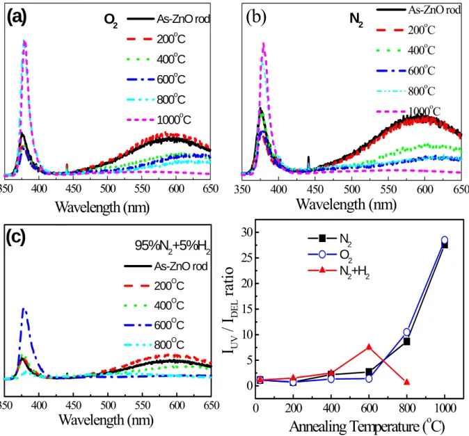
Figure 1 plots the room-temperature photoluminescence spectra of the ZnO nanorods annealed under various conditions. Only two emission peaks at 377nm (UV emission) and 595 nm (visible emission) were observed. It was found that UV emission intensities increase with annealing temperature, but the visible emission in post-annealed samples tends to disappear, suggesting that the native defects or non-radiative recombination can be reduced by post-annealing treatment in O2 and N2 atmospheres as shown in Fig. 1(a) and (b). However,
the ZnO nanorods annealed in N2 show stronger visible emission peaks compared to that
annealed in oxygen atmosphere because the oxygen vacancies become the predominant point defects in N2 atmosphere. In addition, a unique phenomenon was observed for the sample
annealed in H2/N2 atmosphere, as presented in Fig. 1(c). An optimal UV emission occurs at
the 600oC. It was believed that H2/N2 treatment is able to passivate native defects or
impurities that contribute to visible transition, because the hydrogen atoms can be situated in various lattice positions. However, when the sample was exposed to H2/N2 at 800oC, the UV
emission almost disappeared. This marked change can be attributed to the fact that a high-temperature reduction environment of H2/N2 could damage the crystal structure of the
ZnO nanorods by surface etching [9]. Besides, it was also observed that the peak position of the longer-wavelength visible emission band shifts with different treatments. The peak position of the visible (deep-level) emission is related to the predominant defects in the ZnO nanorods and both defects of zinc interstitials and oxygen vacancies are strongly modified by changing annealing temperature and using different atmospheres. The relative PL ratios (IUV/IDLE) of the samples as a function of various atmospheres can be further summarized and
presented in Fig. 1(d), revealing that the improvement in the optical quality of post-annealed ZnO nanorods is not only dominated by the annealing temperature but also the annealing atmosphere.
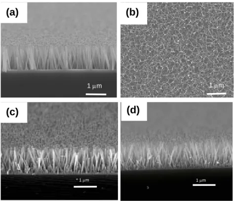
Figure 2(a) shows that the as-grown ZnO nanorods are perpendicular to the substrate with a uniform length of 900-950 nm. As annealed at 600oC in H2/N2, the cross-sectional
morphology of the annealed ZnO nanorods is slightly different from that of the as-grown ZnO nanorods. It was found that the diameter of the annealed ZnO nanorodswas locally necked. When the ZnO nanorods were annealed at 800˚C in H2/N2, the surface image in Fig. 2(b)
shows that all the ZnO nanorods were collapsed on the substrate, probably because of surface etching. These results may elucidate why the UV peak was rapidly and suddenly disappeared at 800˚C in Fig. 1(c). In contrast, as the ZnO nanorods were annealed at 800oC in both O2 and
to that of the as-grown ZnO nanorods (Figs. 2(c) and 2(d)). However, at 1000oC in N2 and O2,
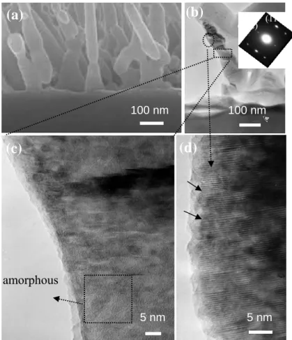
the surface morphology of ZnO nanorods was changed from “rod-like” to irregular shape perhaps because of the melting and re-growth of the nanorods. As shown in Fig. 3(a), HR-TEM of the ZnO nanorods annealed at 1000oC in N2 reveals that the ZnO nanorods were
shortened to 300-400 nm, and became partially joined to their neighbors. The split diffraction spots in the central region of the SAED pattern suggest that the merged ZnO nanorods are not perfectly aligned in either the a (or b) and c directions, as presented in the inset of Fig. 3(b). Moreover, HR-TEM images of the ZnO nanorods in Fig. 3(c) demonstrate that partial amorphous was formed in the single-crystal ZnO nanorod. In addition, several lattice fringes (marked with arrows) appear in the edge of the ZnO nanorod in Fig. 3(d). Furthermore, according to X-ray photoelectron spectroscopy (XPS) analysis (not show here), the atomic ratio of O to Zn was approximately to 0.9 for the nanorods and the single of O2- ions in the oxygen-deficient regions were almost covered by the background signal, this indicating these amorphous regions appeared to contain some structural defects. The primary defect type in the region may be considered as oxygen vacancies as evidenced by PL spectra.
3.2 Annealed MgO-coated nanorods
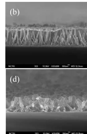
Fig. 4 shows the SEM images taken from several samples with highly uniform and densely packed arrays of MgO-coated ZnO nanorods grown on Si substrate. It can be observed that the surface of as-grown MgO-coated ZnO nanorods, as shown in Fig. 4(a), becomes rough. After annealed at 900oC in O2 and N2 atmospheres, Fig. 4(b) and 4(c) show the MgO-coated
ZnO nanorods still kept hexagonal shape and the morphology of ZnO nanordos remained almost unchanged as compared to that of the as-grown ZnO nanorods [Fig. 2(a)]. However, as annealed at 800 °C in H2/N2, the cross-sectional morphology of the annealed ZnO nanorods in
Fig. 4(d) is obviously different from that of the as-grown ZnO nanorods. Some of the ZnO nanorods annealed at 800°C in H2/N2 are slightly collapsed, probably because of surface
etching.
Fig. 5 shows the X-ray diffraction (XRD) patterns of ZnO and Mg-doped ZnO nanorods annealed at 800°C and 900°C in H2/N2 and N2(and O2). All the XRD patterns indicate the
formation of the wurtzite-type ZnO phase and the same (0 0 2) diffraction peak, implying thathe Zn1-xMgxO nanorods possess the same structure as that of the ZnO with preferentially
orientation in c-axis direction. However, no diffraction peak of MgO crystal or Mg phase was detected in the XRD patterns, indicating that the Mg has been incorporated within the ZnO nanorods by means of substituting Zn.
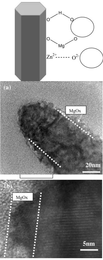
It was postulated that some chemical bonding should exist between the oxide coating particles and the surface of ZnO nanorods, as illustrated in Fig. 6(a). The hydrogen bridges bonding and electrostatic forces played an important role in this process. [10]. On the other hand, part hydrolysis of ZnO nanorods surface was useful to the formation of the bonding.
During the process of hydrolysis, OH- could react with Mg2+, leading to MgO particles adhering better on the surface of ZnO nanorods.
As evidenced from high-resolution TEM (HRTEM) in Fig. 6(b), hetrostructured core(ZnO)-shell(Mg-compound) nanorod were observed. The diameter of the core (ZnO
nanorods) and the shell(MgOx) thin layer is about 25 nm and 7 nm, respectively. Figure 6(c) shows that the {0002} lattice fringe of the ZnO nanorod core was parallel to the basal plane but no any lattice fringe can be identified in shell-MgOxx thin layer, indicating that the shell
layer was amorphous. The EDS analysis in core region presents a strong ZnO signal and no Mg element. In contrast, in shell region, ZnO signal and Mg element were detected. The high-resolution TEM demonstrates that the ZnO nanorods were successfully coated with MgOx layer.
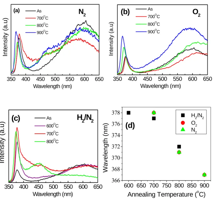
Fig. 7 illustrates the room-temperature photoluminescence (PL) property of ZnO and Zn1-xMgxO nanorods. The ultraviolet (UV) emission peak of ZnO is generally attributed to the
excitonrelated activity, and the deep level emission may be due to the transitions of native defects such as oxygen vacancies and zinc interstitials. A blue shift of the near-band-edge emission was observed when annealing temperature is above 700 oC. These results are in reasonable agreement with the thermal diffusion of Mg atoms at the MgO/ZnO heterointerface, which is observed only after annealing above 700 oC, [11] and with the formation of a Zn1-xMgxO alloy. The UV emission peaks at 371 and 367 nm for the samples
annealed at 800 and 900 oC, respectively, are attributed to the various Mg content in the Zn1-xMgxO alloys formed at the different temperatures in O2, N2 and H2/N2, as presented in
Fig. 7(a), (b) and (c), respectively. It can be found that the blue shift of UV emission seems independent of atmosphere but influenced by annealing temperature. However, a blue shift of the near-band-edge emission of H2/N2 annealing sample is not the same as that of O2 and N2
annealing sample, as shown in Fig. 7(d). Broadband visible emissions are observed in all PL spectra of the nanorods. It was noted that the visible emission from the annealed Zn1-xMgxO
nanorods at 800 oC in H2/N2 is centered at about 454 nm, providing the blue color. It may be
related to the visible emission peak centered at 454 nm, indicating MgO diffusion process produces a new luminescent center in reduced atmosphere. In contrast, the visible emission peak of the ZnO nanorods annealed in H2/N2 is still at about 595 nm, [12] proving the visible
emission peak centered at 454 nm has relation with MgO diffusion.) In contrast, the Zn1-xMgxO nanorods annealed in O2 or N2 exhibits the orange emission centered at about 595
nm. However, visible emission from Zn1-xMgxO nanorods annealed at 700 oC in H2/N2 seems
to include two visible emissions which are centered at 454 and 595 nm. These results indicate that the MgO-coated ZnO nanorods have different luminescent centers in different annealing atmospheres.
Conclusion
changed and controlled by annealing the ZnO nanorods in various atmospheres at different temperatures. For the sample annealed in both O2 and N2 atmospheres, the room-temperature
UV emission of the ZnO nanorods increases with the increase of temperature due to the reduction of structure defects. Structural analyses of Zn1-xMgxO nanorods by XRD indicate
that the hexagonal nanorods grown on Si substrates are oriented in the c-axis direction. As the MgO-coated ZnO nanorods were annealed at above 800 oC, the Zn1-xMgxO alloy may be
formed due to diffusion of the Mg atoms into the ZnO nanorods. A blue shift of the near-band-edge emission with increasing the annealing temperature was observed. It is noted that the visible emission from the Zn1-xMgxO nanorods annealed at 800 oC in H2/N2 is
centered at about 454 nm. In the contrast, the visible emission from the Zn1-xMgxO nanorods
annealed O2 or N2 is at 595 nm. References
[1] C. Weisbuch, H. Benistry, and R. J. Houdre, J. Lumin., 85, 271 (2000).
[2] M. H. Huang, S. Mao, H. Feick, H. Yan, Y. Wu, H. Kind, E. Weber, R. Russo, and P. Yang, Science, 292, 1897 (2001).
[3] Minami, T.; Nanto, H.; Takata, S. Jpn. J. Appl. Phys. 23 (1984) L280. [4] Hu, J.; Gordon, R. G. Sol. Cells, 30 (1991) 437.
[5] Joseph, M.; Tabata, H.; Kawai, T. Appl. Phys. Lett. 74 (1999) 2534.
[6] T. Makno, Y. Sagawa, M. Kawasaki, A. Ohtomo, R. Shiroki, K. Tamura, T. Yasuda, H. Koinuma, Appl. Phys. Lett. 78 (2001) 1237.
[7] S. Raghavan, J.P. Hajra, G.N.K. Iyengar, K.P. Abraham, Thermochim. Acta 189 (1991) 151.
[8] R.D. Shannon, Acta Crystallogr., Sect. A: Cryst. Phys., Diffr., Theor. Gen. Crystallogr. 32 (1976) 751.
[9] L. E. Greene, M. Law, J. Goldberger, F. Kim, J. C. Johnson, Y. Zhang, R. J. Saykall, and P. Yang, Angew. Chem. Int. Ed., 42, 3031 (2003).
[10] N. Arul Dhas, A. Zaban, A. Gedanken, Chem. Mater. 11 (1999) 806.
[11]A. Ohtomo, R. Shiroki, I. Ohkubo, H. Koinuma, M. Kawasaki, Appl. Phys. Lett. 75 (1999) 4088.
[12] C. C. Lin, H.-C. Liao, S. Y. Chen, and S. Y. Cheng. J. Vac. Sci. Technol. B 24 (2006) 304.
Acknowledgments
This work was financially supported by the National Science Council of the Republic of China, Taiwan under Contract No. NSC-94-2216-E-009-025.
350 400 450 500 550 600 650
(a)
O
2Wavelength (nm)
As-ZnO rod 200oC 400oC 600oC 800oC 1000oC 350 400 450 500 550 600 650(b)
Wavelength (nm)
N
2 As-ZnO rod 200oC 400oC 600oC 800oC 1000oC 350 400 450 500 550 600 650(c)
95%N
2+5%H
2 As-ZnO rod 200OC 400OC 600OC 800OCWavelength (nm)
Fig. 1. Room-temperature PL spectra of ZnO nanorods annealed at various temperatures in (a) O2, (b) N2 and (c) H2/N2 atmospheres. (d) IUV/IDEL of
annealed ZnO nanorods dependent on various annealing conditions.
0 200 400 600 800 1000 0 5 10 15 20 25 30
Annealing Temperature (
oC)
N2 O2 N2+H2I
UV/ I
DELratio
Fig. 2. SEM images of (a) as-grown ZnO and annealed ZnO nanorods at 800oC in (b) H2/N2. (c) O2, and (d) N2.
(b)
1 µm 1 µm(d)
1 µm(c)
1 µm(a)
Fig. 3. (a) High-magnification SEM and (b) low-magnification TEM images of ZnO nanorods annealed at 1000oC in N2 ambient with a corresponding
diffraction pattern in the inset. A high-resolution TEM image of (b), showing the selected area in the (c) neck and (d) top of the ZnO nanorod.
100 nm 100 nm 5 nm 5 nm amorphous
(a)
(b)
(c)
(d)
(002) (110)Fig.4 SEM images of (a) MgO-coated ZnO nanorods, and annealed at (b)900oC in N2,
(c) 900oC in O2, and (d) 800oC in H2/N2.
Fig. 5 XRD of MgO-coated ZnO nanorods annealed in various atmospheres.
(a) (b)
(c) (d)
30
35
40
45
50
55
60
In
tensity (a.u)
2
θ
As MgO-coated ZNs (Mg-ZNs) Mg-ZNS/H2/N2 800OC Mg-ZNS/N2 900OC Mg-ZNs/O2 900OCFig. 6 (a) Model of bonding between MgO coating particles and surface of ZnO nanorods. (b) Low-magnification and (c) High-resolution TEM images of MgO-coated ZnO nanorod annealed at 800oC in O2 atmosphere.
MgOx H O O O Mg O Zn2+ O
2-5nm
(b)
(a)
20nm
MgOx MgOxFig 7. Room-temperature PL spectra of ZnO nanorods annealed at various temperatures in (a) N2, (b) O2, (c) H2/N2 atmospheres. (d) UV peak
position of ZnO nanorods dependent on various annealing conditions
600 650 700 750 800 850 900 366 368 370 372 374 376 378