379 IEEE ELECTRON DEVICE LETTERS, VOL. 14, NO. 8, AUGUST 1993
Tunnel Oxide Prepared by Thermal
Oxidation of Thin Polysilicon Film on
Silicon (TOPS)
Shye Lin
Wu,
Member, IEEE, Chung Len Lee, SeniorMember, IEEE, and T a n FuLei
Abstract-This letter presents a textured tunnel oxide, TOPS, prepared by thermally oxidizing a thin polysilicon film on a Si substrate. Due to the rapid diffusion of oxygen through the grain boundaries of the thin polysilicon into Si substrate and the enhanced oxidation rate at the grain boundaries, a textured Si/SiO, interface is obtained. The textured interface results in the localized high fields and enhances electron injection into TOPS. The TOPS exhibits a higher electron injection efficiency, a better immunity to the electron trapping and the interface state generation under the high-field operation, and a higher asymmetric injection polarity as compared to the normal oxide.
I. INTRODUCTION
IN tunnel oxides ( 5 100
A)
or thick polyoxidesI-?
oxides grown on polysilicon, ~ 6 0 0A)
are used as the tunneling gate dielectrics of electrically erasable pro- grammable read-only-memories (EPROM's) [ll. It had been reported that thermal oxides grown on an n f heav- ily-doped silicon substrate exhibited a higher electron conduction efficiency due to the reduction of the effective barrier height at the Si/SiO, interface [2]. Recently, Fonget al. [31 and Hao et al. [41 have also reported that tunnel oxide grown on a pretexturized silicon substrate can achieve the enhanced electron conduction efficiency due to the surface field enhancement.
In this letter, we propose a novel simple method to fabricate a thin textured tunnel oxide with a higher elec- tron conduction efficiency, a lower electron trapping rate, and a highly asymmetric injection polarity.
11. EXPERIMENTAL PROCEDURES
The thin textured tunnel oxide capacitors were fabri- cated on n-type 0.55-1.1 f i ecm (100) Si wafers. Some wafers were heavily doped by using an arsenic ion implan- tation of a dose of 5 X 1015 cm-, at 100 keV through a
500-A pad oxide followed by annealing at 900°C in an N, ambient for 40 min. After removing the pad oxide, a very thin amorphous silicon (a-Si) film ( 5 100
A)
was de- posited on Si wafers at 550°C by using an LPCVD system.Manuscript received March 24, 1993; revised May 25, 1993. This work was supported by the National Science Council of the Republic of China through research contract NSC 81-0404-E009-134.
The authors are with the Department of Electronics Engineering and the Institute of Electronics, National Chiao-Tung University, Hsinchu, Taiwan, Republic of China.
IEEE Log Number 9210890.
In this study, the deposition rate and deposition pressure of a a-Si were controlled at about 20 A/min and 150 mtorr, respectively. The thickness of a-Si film was esti- mated by the deposition rate and deposition time. The wafers were carefully loaded into furnace at 600°C to reduce the thermal stress and to minimize the native oxide growth. The temperature was gradually raised to 900°C in an N, ambient. During the temperature ramp- ing-up step, the a-Si films were crystallized into polysili- con [5]. Then, thin tunnel oxides were grown by com- pletely oxidizing the thin polysilicon films at 900°C in a dry 0, ambient. Due to the rapid diffusion of oxygen through the grain boundaries of thin polysilicon into Si substrate and the enhanced oxidation rate at the grain boundaries, a textured Si/SiO, interface is obtained. As a result, after the polysilicon was completely converted into the oxide, an irregular and textured interface with the Si substrate was formed. This textured tunnel oxide is re- ferred to as TPPS. To characterize the textured tunnel oxide, a 4000-A POC1,-doped polysilicon layer was then deposited on TOPS to form MOS capacitors. For compar- ison, MOS capacitors with the normal oxide were also made at 900°C with a similar thickness as that of TOPS. The effective oxide thickness of TOPS was determined by the high-frequency CV measurement. The transmission electron microscopy (TEM) was used to examine the morphology of the Si/SiO, interface.
111. RESULTS AND DISCUSSION
Fig. 1 shows the TEM micrograph of the cross section of TOPS, where a textured Si/SiO, interface is clearly observed. The textured interface results in the localized high fields and enhances electron injection into TOPS.
Fig. 2 shows the accumulation-mode and inversion-mode Jg-Vg characteristics of TOPS and normal oxide with a thickness of about 100
A.
The thickness of the stacked a-Si is about 50A
and the area of the samples is 2.8 Xcm2. It is seen that the TOPS exhibits a much higher electron conduction efficiency than the normal oxide in both injection polarities. For example, for a constant injection current density of 10 mA/cm2, which is the typical rapid charging of the floating gate [3], the TOPS with the textured interface reduces the gate voltage from
380
Fig. 1. TEM micrograph of the cross section of TOPS.
v g (Volts)
Fig. 2. The accumulation-mode and inversion-mode Jg-Vg characteris-
tics of TOPS and normal oxide of 110 8, thickness grown on the lightly doped substrate.
about 11.2 V of the normal oxide to about 5.5 V for the accumulation-mode Jg-l/g characteristics.
It is interesting that, as shown in Fig. 1, the degree of the texturization of the Si/SiO, (bottom) interface is much larger than that of the poly-Si/SiO, (top) interface. Hence, the electron injection from the bottom interface into TOPS is much more efficient than from the top interface. For example, the current density at = 5 V of electron injection from the bottom interface is about five orders in magnitude larger than that of electron injection from the top interface. The asymmetrical characteristics have special advantages for the EEPROM device applica- tion.
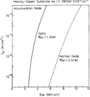
Fig. 3 shows the J,-E,, characteristics of TOPS (160
&
and normal oxide (180A)
grown on the heavily doped substrate. The thickness of the stacked a-Si is about 75A.
It is seen that the enhanced electron injection efficiency becomes more significant. This is due to the textured Si/SiO, interface of TOPS, in conjunction with the sub- strate heavy doping effect [21.
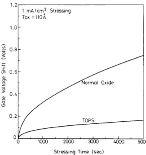
Fig. 4 shows the curves of the gate voltage shift (AV,)
versus the stressing time of TOPS and normal oxide under
IEEE ELECTRON DEVICE LETTERS, VOL. 14, NO. 8, AUGUST 1993
Heavily-Doped Substrate As I I I lOOKeV 5 ~ 1 0 ' ~ c r n - ~
Eox (MVIcrn)
Fig. 3. The Jg-Dox characteristics of TOPS (160 A) and normal oxide (180 A) grown on the heavily doped substrate. The measurement polarity is in accumulation mode.
-
Before stressing After 10 rnA/crnZ Str 8 0, 0 -3 -2 -1 0 1 v g (Volts)Fig. 4. The curves of the gate voltage shift (AV,) versus the stressing
time for TOPS and normal oxide under a constant current stressing of 1 mA/cm2 for 5000 s.
a constant current stressing of 1 mA/cm2 up to 5000 s (in
accumulation mode). It is seen that both oxides exhibit an electron trapping behavior, however, the TOPS exhibits a
AVg of 4 times lower than that of the normal oxide. This
implies that TOPS has a better immunity to the electron trapping under a high-field operation. This may be be- cause for the TOPS, a lower bulk electric field existed which consequently generated less electron-hole pairs as compared to the normal oxide [3]. This lower bulk electric
WU et al.: TUNNEL OXIDE PREPARED BY THERMAL OXIDATION OF POLYSILICON FILM ON SILICON 381
1.2
1 mA/cmq* Stressing Tox = l l O A
Stressing Time (sec)
Fig. 5. The quasi-static CV characteristics of TOPS and normal oxide before and after 10-mA/cm2 stressing for 100 s.
field further increases the stressing endurance of TOPS. Fig. 5 shows the quasi-static CV (QSCV) characteristics of TOPS and normal oxide before and after a constant current of 10-mA/cm2 stressing for 100 s. For the TOPS, there is no significant degradation in the QSCV curve after stressing.
IV. CONCLUSION
The TOPS tunnel oxide presented in this letter is very simple to fabricate and offers a much higher electron conduction efficiency, smaller electron trapping rate, and less associated interface state generation.
REFERENCES
S. K. Lai, V. K. Dham, and D. Guuterman, “Comparison and
trends in today’s dominant E 2 technologies,” in IEDM Tech. Dig., 1986, p. 580.
H. Nozawa, N. Matsukawa, and S. Morita, “An EEPROM cell using a low barrier height tunnel oxide,” IEEE Trans. Electron Devices, vol. ED-33, p. 215, 1986.
Y. Fong, A. T-T Wu, and C. Hu, “Oxides grown on textured single-crystal silicon-dependence on process and application in EEPROM’s,’’ IEEE Trans. Electron Devices, vol. 31, p. 583, 1990. M. Y . Hao and J. C. Lee, “Electrical characteristics of oxynitrides grown on textured single-crystal silicon,” Appl. Phys. Lett., vol. 60, p. 445, 1992.
T. Karnins, Polycrystalline Silicon for Integrated Circuit Applications. Boston: Kluwer Academic, 1988.