不同成長溫度下高銦組成氮化銦鎵奈米點之光學特性研究
69
0
0
全文
(2) 不同成長溫度下高銦組成氮化銦鎵奈米點之 光學特性研究 Optical properties of In-rich InGaN dots grown at different temperature 研 究 生:楊沛雯. Student:Pei-Wen Yang. 指導教授:李明知 教授. Advisor:Prof. Ming-Chih Lee. 國立交通大學 電子物理研究所 碩士論文. A Thesis Submitted to Institute of Electrophysics College of Science National Chiao Tung University In Partial Fulfillment of the Requirements For The Degree of Master of Physics in Electrophysics July 2007 Hsinchu, Taiwan, Republic of China. 中華民國九十六年七月.
(3) 誌謝 回想過去的兩年研究生活很辛苦也很充實,如今終於完成了碩士學業,首要 感謝對我照顧有加並且在撰寫論文時提供寶貴建議與指教的李明知教授,實驗 上要求嚴謹實事求是私下很關心學生的張文豪老師,平日不斷給我鼓勵與支持 的陳衛國老師以及給我許多意見的周武清老師;從你們身上獲得到的不僅僅只 有學識更有那做人處事的態度,謝謝你們的指導才得以順利完成此篇論文。 再來,我要感謝實驗室的各位兄弟姐妹們。平日實驗時,meeting 報告完總 給我許多意見的學長姊:李寧、京玉、伩哲、林萱、阿邦、繼祖、狗哥;總能 將實驗室填滿歡笑聲並陪伴我一起打拼的同學:一山不容惡少甫、書江鳥、laba 毅、小葳、desk、老包;在我遇到瓶頸最需要關心能立即伸出援手的貼心學弟: 聖允、喵賢、阿德、毛頭、馬先生;真的很謝謝你們對我的照顧與關心。 在這風大到難免感到有些心冷的城市裡,我特別要感謝陪我一起走過這些歲 月的貼心好友們:小佩、苔綿、慈、菲比、學、阿吉、龜泰、老羅、玉倩、筱 筑;擁有你們的熱情包圍,心從此不再寒冷! 最後,我要感謝永遠都很支持我的父母、老哥以及親友團,更要感謝我的天, 並將這份榮耀獻給最疼愛我的爺爺!在此,並以『人生不總是順遂,當我們不 能選我們所愛時,一定要愛我們所選!』一句話與諸位共勉之。 2007 年 7 月 撰於新竹.
(4) Index Acknowledgment Abstract (Chinese version) ………....................................................................i Abstract (English version) …………..............................................................iii Chapter 1 Introduction ……….........................................................................1 Chapter 2 Theoretical backgrounds ……….................................................3 2.1 InGaN structure ………………………………………….................3 2.2 Photoluminescence in semiconductors ……………..........................4. Chapter 3 Experimental ………….................................................................11 3.1 Sample preparations ………………................................................11 3.2 Atomic force microscopy (AFM) ………........................................13 3.3 Macro-photoluminescence (Macro-PL) …......................................16 3.4 Near-field scanning optical microscopy (NSOM) …......................19 3.5 Time-Resolved Photoluminescence (TRPL) …..............................22. Chapter 4 Results and discussion ………....................................................24 4.1 Surface morphology of InGaN dots …............................................24 4.2 X-ray diffraction (XRD) spectrum of InGaN dots …......................29 4.3 Optical properties of InGaN dots ……............................................33 4.3.1 The Macro -PL spectrum results...................................................33 4.3.2 The NSOM spectrum results.........................................................37 4.4 The visible emission band …….......................................................39.
(5) 4.4.1 Excitation wavelength-dependence...............................................39 4.4.2 Excitation power-dependence.......................................................43 4.4.3 Time-resolved photoluminescence (TRPL)..................................48 4.5 Summary of transitions in visible emission band.............................55. Chapter 5 Conclusions ……………................................................................57 References…………….........................................................................................59.
(6) 不同成長溫度下高銦組成氮化銦鎵奈米點之 光學特性研究. 研究生:楊沛雯. 指導教授:李明知 教授. 國立交通大學 電子物理研究所. 中文摘要 本論文中,我們主要探討利用金屬有機化學氣相沉積法在不同成長溫度下之 高銦組成氮化銦鎵奈米點的表面形貌、組成變化以及其光學特性研究。 由原子力顯微鏡影像顯示,當氮化銦鎵奈米點成長溫度由550提升至725 oC 9. 7. -2. 時,該奈米點所呈現出的平均密度由4.0×10 降低至2.2×10 cm 。關於此現象 可歸因於銦原子本身具有較長的遷移長度,導致成長溫度上升時在氮化鎵表面 形成的奈米點平均密度降低。此外,經由X光繞射光譜之譜峰位置結果,可推 估三元合金氮化銦鎵奈米點的銦組成含量由85 %增加至99 %。我們發現此銦組 成範圍所對應的能隙能量與光激螢光光譜之發光位置(0.77至0.92 電子伏特) i.
(7) 互相吻合,進而可確認紅外光螢光訊號來自於氮化銦鎵奈米點,並且與銦組成 含量有關。另外,由X光繞射光譜之半高寬與紅外光光激螢光光譜之積分強度 比較顯示,較高溫成長之樣品具有良好的發光品質。 o. 除此之外,由螢光光譜中發現,當樣品成長溫度高於650 C亦同時存有可見 光螢光訊號,其頻譜分佈在2.0至2.4電子伏特。我們藉由近場光學顯微系統檢 驗發現,此可見光螢光訊號乃源自於氮化銦鎵奈米點外的區域。然而,可見光 螢光訊號強度隨著改變激發能量漸高於氮化鎵能隙能量而增加,發光位置亦隨 著激發功率增加而產生藍移現象。綜合以上兩結果,我們認為此可見光訊號的 躍遷方式可能是樣品成長過程中形成氮化鎵缺陷帶,致使其中施子-授子之能 階躍遷,亦或是自由電子至深層束縛授子能階的躍遷行為。在載子生命週期部 分,我們觀察到兩段時間常數,並推測短時間來自於淺層授子能階載子以垂直 躍遷且非經由聲子散射之輻射復合時間,長時間則屬於載子在深層侷域態或以 非垂直躍遷以之輻射復合時間。. ii.
(8) Optical properties of In-rich InGaN dots grown at different temperature. Student:Pei-Wen Yang. Advisor:Prof. Ming-Chih Lee. Institute of Electrophysics National Chiao Tung University. Abstract In this thesis, we investigated the surface morphologies, alloy composition, and optical properties of In-rich InxGa1-xN dots (x>0.85), which were prepared at different growth temperature (Tg) by metalorganic chemical vapor deposition (MOCVD). The atomic force microscopy (AFM) images showed that the InGaN dots density decreased from 4.0×10⁹ to 2.2×107 cm-2 as the Tg was increased from 550 to 725 oC. This can be attributed to the enhanced migration length of In adatoms that resulted in the formation of less dense dots. The X-ray diffraction peak of ternary InGaN shifted gradually toward the InN (0002) as Tg was increased until 725 °C, hence the. iii.
(9) In content increased from x = 0.85 to 0.99. The calculated band gap is consistent with the photoluminescence (PL) peak position ranging from 0.77 to 0.92 eV, which is attributed to the emission from InGaN dots with different In compositions. For Tg > 650 oC, another visible emission band around 2.0 - 2.4 eV was observed. By near-field scanning optical microscopy (NSOM) mapping, we found that the visible emission band emerged from the region outside the In-rich InGaN dots. The integrated PL intensity increased with tuning to above the band gap excitation that suggested GaN related-defect levels are involved for recombination of photo-generated carriers. Furthermore, a blueshift of the visible peak position with the increasing photoexcitation power density was observed. This can be interpreted by the donor–acceptor pair (DAP) or free to bound (FB) transition model. Time-resolved PL shows two decay components, in which the fast decay constant (τ1) represents radiative recombination time of carriers in shallower potentials or via vertical transitions without involving phonons scattering , while the slower one (τ2) was accounted for radiative recombination in deeper localized states or non-vertical transitions.. iv.
(10) Chapter 1 Introduction Recently, group-III nitrides such as AlN, GaN, InN and their alloys have become one of the most important materials for semiconductor optoelectronic devices. In particular, the importance are heterostructures incorporating ternary InGaN alloys, which have been used in a variety of commercial optoelectronic devices, including blue-green and ultraviolet spectral ranges light emitting diodes (LEDs) and laser diodes [1]. In the early 1990s during the development of GaN-based devices, the band gap of InxGa1−xN thin films with increasing values of x has been investigated. One report found that the energy gap decreased very rapidly with increasing In content and fell well below 2 eV for x = 0.5, suggesting that the energy gap of InN is significantly less than 1.9 eV [2, 3]. Although it is quite convenient to select the emission region by controlling the indium content, the growth of InGaN alloys, particularly with high In content, remains of great challenge. The difficulty arises not only from the high vapor pressure of N2 over InN [4], but also from the large lattice mismatch between InN and GaN (~11%). Since indium-containing compounds are unstable with due to In segregation, it has been argued that self-organized nanometer scale In-rich quantum dots (QDs),. 1.
(11) originated from In-segregation taking place in the InxGa1−xN alloys, are the source of a radiative recombination channel emitting in the blue-green region of the spectrum [5, 6]. Up to now, InGaN-based devices are suitable UV-blue-green light emitters but they are much less efficient for near infrared emission [7]. In this context, self-assembled island growth of InGaN/GaN dots appears to be a more controllable way for realizing such In-rich nanostructures [8] which offers a potential alternative for near infrared light emission from the III-nitride device structure. This is our motivation to study this ternary material. However, the InxGa1−xN dots reported to date are still in the Ga-rich side (x < 0.5), with typical emission wavelength in the blue-green range. Thus, the studies on the In-rich side (0.5< x <1) of InxGa1−xN dots with NIR emissions will be needed. In this thesis, we investigated In-rich InxGa1−xN dots (with x>0.85) grown at various temperatures by MOCVD. Atomic force microscopy (AFM), x-ray diffraction (XRD), photoluminescence (PL), near-field scanning optical microscopy. (NSOM). and. time-resolved. photoluminescence. (TRPL). measurements are employed to study the correlation among surface morphologies, alloy compositions, PL emission bands and carrier lifetime of these InGaN dots samples.. 2.
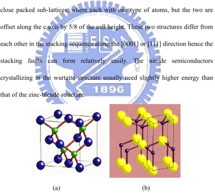
(12) Chapter 2 Theoretical backgrounds 2.1 InGaN structure Ternary InGaN, as well as binary GaN can be formed by two crystalline structures, i.e, wurtzite and metastable zinc-blende structures, as shown in Fig. 2-1-1. The wurtzite structure is a stable phase that consists of two hexagonal close packed sub-lattices, where each with one type of atoms, but the two are offset along the c axis by 5/8 of the cell height. These two structures differ from each other in the stacking sequence along the [0001] or [111] direction hence the stacking faults can form relatively easily. The nitride semiconductors crystallizing in the wurtzite structure usually need slightly higher energy than that of the zinc-blende structure.. (a). (b). Fig. 2-1-1 Schematic diagram of (a) Zinc-Blende structure and (b) Wurtzite structure. 3.
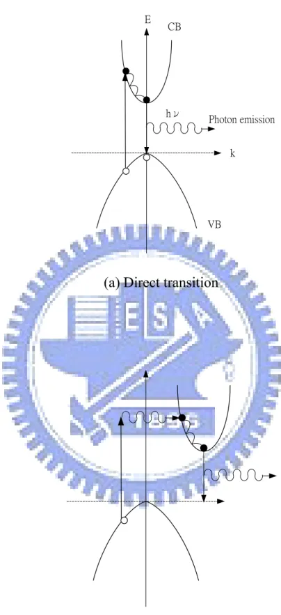
(13) 2.2 Photoluminescence in semiconductors Photoluminescence (PL) is a useful optical method for characterizing semiconductor. It is powerful and sensitive to find impurities and defects, which affect the material quality and device performance. The excitation beam has a photon energy larger than the band gap. In steady state, the photo-generated electrons (holes) relax to the bottom (top) of the conduction (valence) band rapidly, primary via the phonons scattering. The carriers then recombine and produce luminescent photons under the quasi-thermal equilibrium. Two types of recombination are described as follows:. (Ⅰ) Radiative recombination ( a ) Band to Band transition In perfect semiconductors, the excited electrons and holes will accumulate at the conduction band minimum and valence band maximum. For direct band gap semiconductors as shown in Fig. 2-2-1(a), electron-hole pairs (EHP) will recombine without change in its k vector so that this transition is quite probable by satisfying the momentum conservation. But in indirect band gap semiconductors see Fig. 2-2-1(b), the minimum of conduction band (CB) is not directly above the maximum of the valance band (VB) that means change in k vector is necessary. The relaxed carriers at the CB local minimum then via. 4.
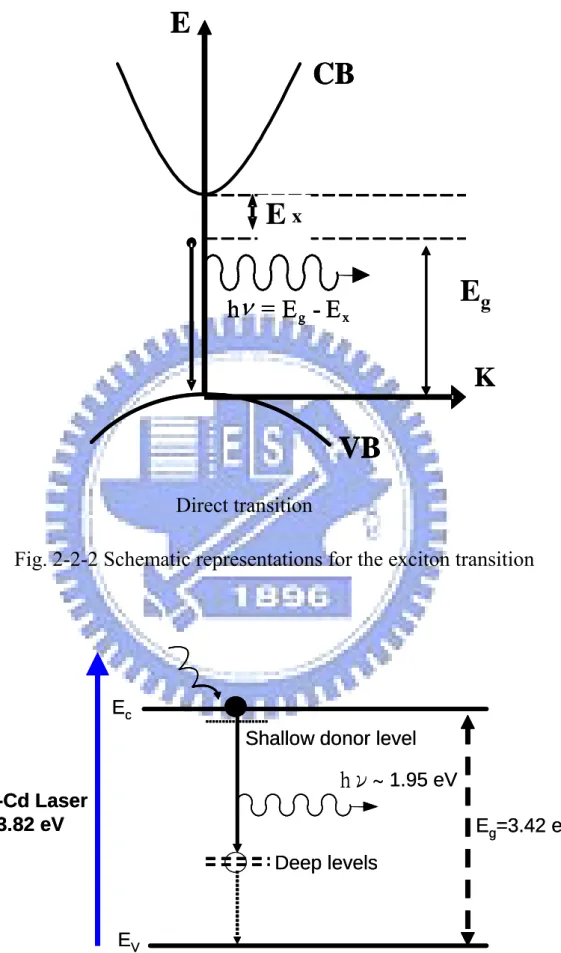
(14) phonon collisions recombine to give photoluminescence. Thus, the transition probability is significantly reduced as compared to direct band gap semiconductors.. ( b ) Exciton transition If the material is sufficiently pure, the Coulomb interaction between the conduction band electrons and the valence band holes will result in the formation of bound electron-hole pairs, called excitons. The exciton may also recombine to emit a narrow spectral line, see Fig. 2-2-2. The emitted photon energy in direct bandgap semiconductors can be expressed as: hν = E g - E x. , Ex =. E0 n2. (1). where Ex is the exciton binding energy; hence the free-exciton emission consists of narrow lines at E g - E x .. ( c ) Free-to-Bound Transition Taking GaN as an example, some research reported that lots of deep levels may be caused by the Ga vacancy or other point defect during the crystal growth process. Such native isolated defects, vacancies, interstitial, and antisite could act as an acceptor. The energy level of VGa was estimated to be 1.5 eV from the. 5.
(15) report [9]. In n-type GaN, the Ga vacancy is filled with electrons, and easy to capture a photo-generated hole, during PL measurements, in which the radiative transition of an electron from the conduction band or from a shallow donor level to the deep level of VGa, (see Fig. 2-2-3).. ( d ) Donor-Acceptor Pair, DAP Transition Impurities presented in semiconductors may form donor (positive) or acceptor (negative) levels in the energy gap. Electrons and holes created by the laser +. -. excitation may be trapped by the donor (D ) and the acceptor (A ) to form the 0. 0. neutral donor (D ) and acceptor (A ). If the neutral donor electron and the acceptor hole recombine, it could emit a photon and return to the ground state as expressed by: 0. 0. +. D + A → hν+ D + A. -. (2). The energy of the photon resulting from radiative recombination can be described by the following formula: hν = E g - (E A + E D ) +. q2 4πεrDA. (3). where Eg is the energy gap of semiconductor, ED and EA are the donor and acceptor binding energies, respectively, ε is the low frequency dielectric constant, and q is the electron charge. The fourth term reflects the Coulomb. 6.
(16) energy of the ionized centers after the recombination, which depends on the distance rDA. With the increasing excitation density, the number of excited donor and acceptor centers increases and their average distance rDA decreases accordingly so that a blue shift of the emission is resulted. In this thesis, the PL spectra of InGaN dots were interpreted by both the DAP and free to bound transitions in the visible and band to band transition in the near infrared ranges.. 7.
(17) E. CB. hν. Photon emission k. VB. (a) Direct transition. (b) Indirect transition Fig. 2-2-1 Schematic representations for the band to band transition. (a) Direct transition and (b) Indirect transition. 8.
(18) E CB. E Exx hν = E g - E x. Eg K. VB Direct transition Fig. 2-2-2 Schematic representations for the exciton transition. Ec Shallow donor level. hν~ 1.95 eV He-Cd Laser E=3.82 eV. Eg=3.42 eV Deep levels. EV. Fig. 2-2-3 Schematic energy level diagram of free to bound transition.. 9.
(19) (Ⅱ) Non-radiative recombination In addition involves to the radiative recombination, majority of energy relaxation non-radiative recombination in which to photon emission occurs. Several transitions that compete with the radiative recombination are depicted as follows:. (a) Phonon emission: Frequently, the electron-hole pair scatters with the lattice vibration and loses its energy by exciting various phonon modes.. (b) Surface recombination: During crystal growth, dangling bonds appeared quite common at the surface and interface, which may capture impurities from the ambient, producing deep and shallow levels. They usually act as recombination centers to relax excess energy from hot carriers. Such recombination centers are likely formed at defect, dislocation, grain boundary or surface irregularity.. (c) Auger effect: As the energy is released by an excited electron, it may be absorbed by another electron immediately to cause energy dissipation, though its probability is significant only at high carrier concentration.. 10.
(20) Chapter 3 Experiments In this chapter, we describe the sample preparation of InGaN dots and then the experimental. systems. such. as. atomic. force. microscopy. (AFM),. photoluminescence (PL), near-field scanning optical microscopy (NSOM) and time-resolved photoluminescence (TRPL).. 3.1 Sample preparations The InGaN dot samples were grown on sapphire (0001) by MOCVD using trimethylgallium (TMGa), trimethylindium (TMIn), and NH3 as source materials. After the growth of a 2-μm-thick undoped GaN buffer layer at 1120 °C, the substrate temperature was decreased to 550 ~ 750 °C to grow InGaN dots by using modulated precursor injection schemes, see Table 3-1-1 and Fig.3-1-1. The precursor flow rates were 2, 150 and 18,000 SCCM (denotes cubic centimeter per minute at STP) for the TMGa, TMIn and NH3, respectively. During TMGa and TMIn flow periods, the NH3 background flow rate was controlled at 10,000 sccm.. 11.
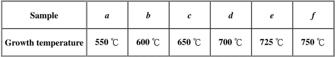
(21) Sample. a. b. c. d. e. f. Growth temperature. 550 ℃. 600 ℃. 650 ℃. 700 ℃. 725 ℃. 750 ℃. Table 3-1-1 The growth condition of InGaN dots.. InGaN dots. HT-GaN (~1120 ℃; 2 μm) LT-GaN Sapphire (001). Fig. 3-1-1 Schematic structure diagram of InGaN dots sample.. 12.
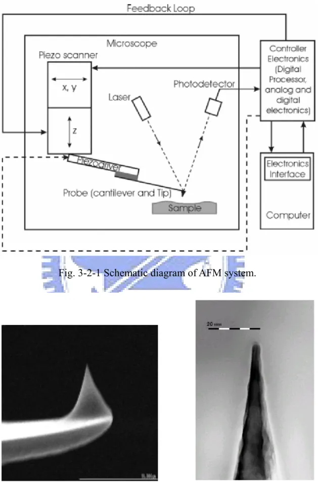
(22) 3.2 Atomic force microscopy (AFM) In the early 1986s, Gerd Binning and Calvin F. Quate invented atomic force microscopy (AFM) and realized that it is able to measure the interactive force between atoms of the probe tip and sample surface by using special probe which consists of a flexible, elastic cantilever and sharp tip. Fig. 3-2-1 shows the configuration of AFM. The sharp tip locates at the free end of a flexible cantilever attached to the scanner. The scanner controls two independent movements of the cantilever: scanning along the sample surface (X-Y plane) and movement perpendicular to the surface (along the Z-axis). The scanner is made of piezoelectric material that expands or shrinks depending on the applied voltage. When the cantilever is bent by the repulsive or attractive force from the interaction between the tip and the sample surface, it changes the deflection. During scanning, the detection system measures the cantilever deflection from its initial position and then sends a signal proportional to the deflection to the scanner control system. The feedback signal is used to move the probe up or down by the piezoelectric crystal to bring the parameter back to its original values. Simultaneously, the probe displacement is recorded by computer and interpreted as the specimen topography. There are three operation modes in AFM, i.e. contact, non-contact, and. 13.
(23) tapping mode. Contact mode has the highest resolution of all three modes in which the tip touches the surface and scans over the sample. But in this way, the tip or sample may easily be damaged by the scanning process. Non-contact mode is preferred to avoid the probe deformation since it utilizes the long range Van der Waal’s force between the tip and specimen. However, the sensibility and resolution is limited in the interference from ambient environment. Tapping mode is the compromise of the above, which consists of contact and non-contact mode. Detection of tapping mode is more sensitive than that in non-contact mode and less destructive on probes or specimen than that in contact mode. Scanning probe microscopy (SPM) system used in our lab is Slover P47H, manufactured by the “Molecular Devices and Tools for Nano Techology (NT-MDT)” in Russia. It can be operated in multi-modes such as AFM for morphology measurements. In our studies, the InGaN dots morphology was measured by tapping mode in order to optimize the resolution and avoid probe destruction. The AFM probe, which has a cantilever about 50 or 80 μm and a sharp tip with a radius of curvature about 10 nm (Fig. 3-2-2), is also from NT-MDT.. 14.
(24) Fig. 3-2-1 Schematic diagram of AFM system.. Fig. 3-2-2 The SEM image of scanning probe and the tip.. 15.
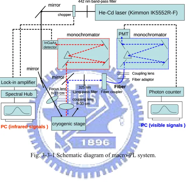
(25) 3.3 Macro-photoluminescence (Macro-PL) Macro-PL system consists of two parts, one for the infrared range and the other for visible signals as shown schematically in Fig. 3-3-1.. I. The infrared signals: For infrared signals, a He-Cd laser (Kimmon IK5552R-F) operating at 442 nm lines was used as the excitation light source with maximum output power ~ 92 mW. The beam passed through a 442 nm band-pass filter to ensure that the excitation source is pure from 400 nm to 2000 nm. The laser beam which was focused by a f=15 cm lens onto the sample, with a beam size ~250 μm. The luminescence signals were collected by lens, in which the laser intensity was blocked by a 850 nm long- pass filter (Thorlabs), and then coupled into a monochromator (ARC Pro 500). The dispersed signals were detected by a extended InGaAs detector (EOS), and processed using a lock-in amplifier (Stanford SR530), and then sent into Acton Spectra Hub for PL analysis.. II. The visible signals: Laser operating at the 325 nm UV line was used as the excitation light source with the maximum output power ~ 22 mW. The configuration of PL in visible region is similar to the infrared, except that the luminescence signals are reflected by a UV mirror and feed into a optical fiber, which was finally coupled. 16.
(26) into the monochromator (ARC Pro 500). The signals were dispersed by the monochromator, whose spectral resolution is about 0.25 nm when both the entrance and exit slits where opened to 250 μm. The dispersed signals were detected by a photomultiplier tube (Hamamatsu R943-02) using the normal applied voltage -2000 V, along with a photon counter (Hamamatsu C1230) for detection. Low-temperature macro-PL was carried out using a closed cycle cryogenic system (APD HC-2D). The temperature was varied from 13 K to 300 K by Lakeshore 330 temperature controller.. 17.
(27) 442 nm band-pass filter. mirror. He-Cd laser (Kimmon IK5552R-F). chopper. monochromator. PMT. monochromator. InGaAs detector. mirror Coupling lens. mirror Lock-in amplifier Spectral Hub. Focus lens f=15 cm. Fiber adaptor. Fiber 325 nm Long-pass filter Fiber coupler. Photon counter. coupling lens f=30 cm. PC (infrared signals ). cryogenic stage. PC (visible signals ). Fig. 3-3-1 Schematic diagram of macro-PL system.. 18.
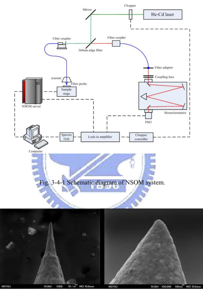
(28) 3.4 Near-field scanning optical microscopy (NSOM) The optical coupling system and the scanning probe are the most important parts of NSOM measurements, which are described respectively in this section.. I. Experimental setup Fig. 3-4-1 showed the schematic diagram of NSOM system. The scanning measurement was performed with Solver SNOM (Olympus based) developed by NT-MDT. A He-Cd laser (Kimmon) operated at the 325nm is used as the excitation light source which is reflected from the edge filter (Semrock, LP02-364RU) then coupled into the optical fiber and illuminated on the sample through the probe. The PL signals were collected by the same probe and passed through the edge filter that blocked the excitation laser beam. The PL signals were dispersed by the monochromator (ARC Pro 500) and detected by the Hamamatsu R955 photomultiplier tube. The PMT signals were processed by the lock-in amplifier (Stanford SR530) and the Solver SNOM controller. Our system collected the PL signals and topography images at the same time to show the NSOM mapping image.. II. Fabrication of NSOM probe The optical probe is the most critical part of the near-field microscope for achieving high resolution images. NSOM probes have been fabricated from a. 19.
(29) variety of materials, including cleaved crystal, semiconductor structures, glass pipettes, and tapered optical fibers [10]. Following fabrication of the tapered tip, the sides of the probe are coated with an opaque metal film (usually aurum, platinum, or aluminum) to prevent light loss in regions of the waveguide other than the aperture. There are many different ways to fabricate and characterize near-field optical probes. There are a variety of techniques that have proven to be useful for fiber tapering, but the task is most commonly accomplished by chemical etching or by heating and pulling, and in some cases both methods are combined to achieve the desired taper characteristics. Our NSOM probe was made by chemical etching of BOE solution (HF: NH4F = 1:6) and coated with platinum metal film by using ion sputter (Hitachi E-1010). Then, the probe was adhered to a tuning fork with the resonance frequency at 32.768 KHz. Fig. 3-4-2 showed the SEM image of coated tip.. 20.
(30) Fig. 3-4-1 Schematic diagram of NSOM system.. Fig. 3-4-2 The SEM image of coated tip. 21.
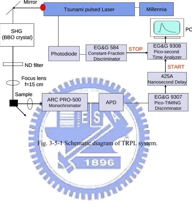
(31) 3.5 Time-Resolved Photoluminescence (TRPL) For TRPL measurements, the excitation pulse of width about 120 fs and the repetition rate locked to the frequency of 80 MHz was generated from a mode-locked Ti:Sapphire laser (Tsunami). Its output beam at λ=700~720 nm was frequency-doubled to the UV region by a BBO (Beta Barium Borate ) crystal. The laser beam was focused by a f = 15 cm focusing lens onto the sample to a spot about 500 μm in diameter, then we used a 400 nm long-pass filter (10LWF-400-B) to remove the second harmonic light. The TRPL signals were dispersed through a single-grating monochromator (ARC Spectro PRO-500) with a 1200 lines/mm grating and detected by an avalanche photodiode (APD), which are then sent to the picosecond timing discriminator (EG&G-9307) to define the arrival time. The delay line (EG&G-425A) is incorporated to postpone the signals long enough to arrive at the picosecond time analyzer (PTA EG&G-9308) after 50 ns interpolation dead time as the Start pulse. The reference frequency of 80 MHz is directly sent to the constant fraction discriminator (EG&G-584) and then marks the arrival time of the analog pulse by sending a timing logic pulse to the Stop input of the picosecond time analyzer (PTA EG&G-9308). Finally, the signals were received by a GPIB card and recorded by a computer for data processing.. 22.
(32) Mirror Millennia. Tsunami pulsed Laser. PC. SHG (BBO crystal) EG&G 584 Photodiode. Constant-Fraction Discriminator. STOP. EG&G 9308 Pico-second Time Analyzer. ND filter. START 425A. Focus lens f=15 cm. Nanosecond Delay. Sample. EG&G 9307. ARC PRO-500. APD. Monochromator. Pico-TIMING Discriminator. Fig. 3-5-1 Schematic diagram of TRPL system.. 23.
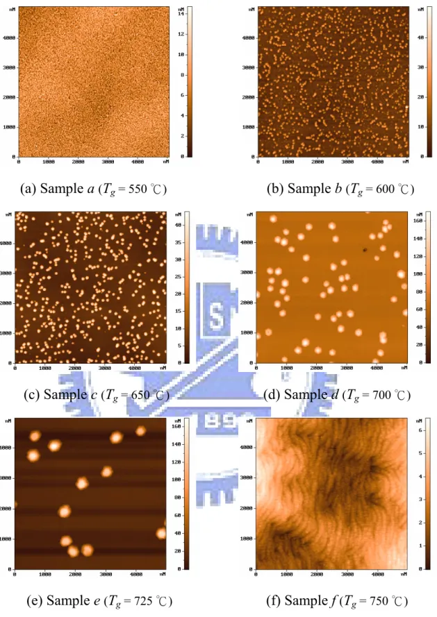
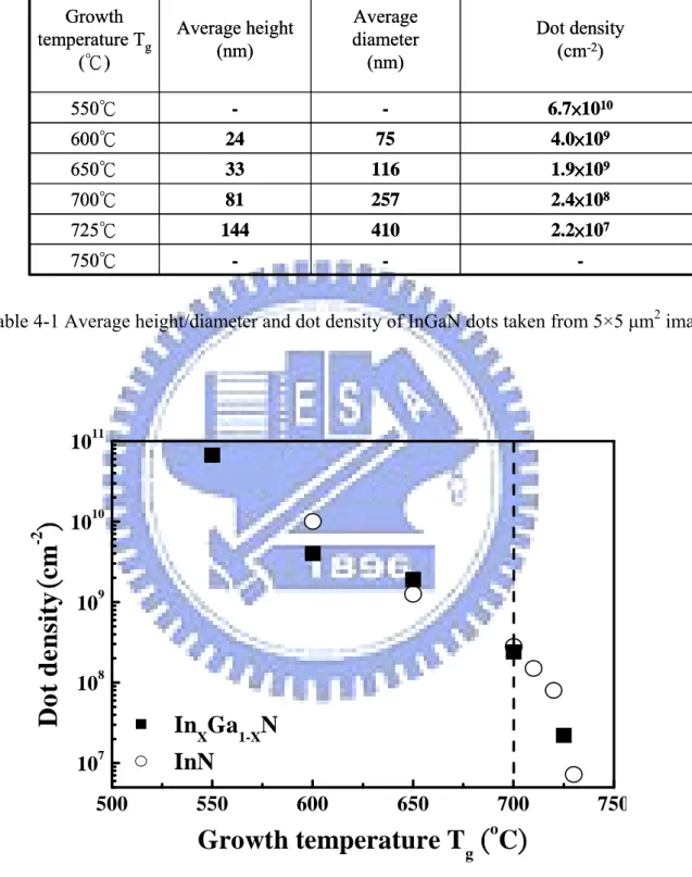
(33) Chapter 4 Results and discussion In this chapter, we will discuss the surface morphologies, alloy compositions and emission properties of these In-rich InxGa1-xN dots (x >0.87) depending on growth temperature by AFM, XRD, PL, NSOM, and TRPL measurements. Not only the NIR emission but also the visible emission was observed, in which NIR signals agree with XRD results. Furthermore, NSOM mapping of the visible emission provided the spatial correlation with the non-dot region from AFM morphologies. Finally, we will propose an energy scheme to explain both the NIR and visible emissions as shown in PL spectra.. 4.1 Surface morphology of InGaN dots As shown in AFM images of Fig. 4-1-1, the sample grown at 550 °C appears to be a rough film formed by coalescent islands. For growth temperatures in the range of Tg = 600-725 °C, individual InGaN dots were observed. With the increasing Tg, the average height and diameter of the InGaN dots increased from 24 to 144 nm and 75 to 410 nm, respectively; whereas the dot density decreased from 4.0×10⁹ to 2.2×107 cm-2, see Table 4-1 and Fig. 4-1-2. For Tg between 600 and 700 °C, the decreasing dot density with the increasing Tg can be attributed to. 24.
(34) the enhanced migration length of adatoms between In and Ga adatoms, that resulted in the formation of much larger and less dense dots at higher growth temperatures [11]. For Tg > 700 °C, the dot density decreased rapidly and dropped to zero at 750 °C, due possibly to the desorption of metallic In from the growing surface. To further study the nucleation mechanism of InGaN dots, we have also prepared a series of samples with InN dots grown at different Tg under similar growth conditions. The density of InN dots as a function of Tg was also included in Fig. 4-1-2. We found that the densities of InGaN and InN dots show a similar dependence on Tg, implying that the nucleation of InGaN dots is governed by the surface migration of In adatoms, rather than Ga or both. This can be realized from the very different migration capabilities of In and Ga adatoms on the GaN surface. Since the bond strength of InN (7.7 eV/atom) is weaker than GaN (8.9 eV/atom), In adatoms (or its adsorbed precursor molecules) are expected to have a considerably longer migration length on the GaN surface, leading to a much higher nucleation rate and hence governing the formation of InGaN dots. This increasing trend is also a consequence of the different migration capabilities of In and Ga adatoms, which considerably hinders the incorporation of Ga into InN islands to form InGaN alloys. Because the Ga migration length is. 25.
(35) relatively shorter, they are unable to travel long enough to reach the already formed InN islands (or In-rich InGaN islands) during the deposition periods of TMIn and TMGa. This effect is expected to be more pronounced at higher growth temperatures, due to the even larger difference in their migration capability. For the case of 725 °C grown sample, the InxGa1−xN dots become highly In-rich, with x up to 0.99. Therefore, it can be inferred that most of the deposited Ga adatoms are very likely to be distributed among these In-rich islands, forming a thin Ga-rich layer. We would like to point out that the deduced In content from Fig. 4-1-2 does not follow the prediction of equilibrium solubility of GaN in InN [12], where the Ga content is expected to increase with the growth temperature based on thermodynamic considerations. This implies that the incorporation of Ga into InN during the growth of InGaN dots is kinetically inhibited, rather than under thermodynamic equilibrium.. 26.
(36) (a) Sample a (Tg = 550 ℃). (b) Sample b (Tg = 600 ℃). (c) Sample c (Tg = 650 ℃). (d) Sample d (Tg = 700 ℃). (e) Sample e (Tg = 725 ℃). (f) Sample f (Tg = 750 ℃). Fig. 4-1-1 AFM morphology images of InGaN dots. 27.
(37) Growth temperature Tg (℃). Average height (nm). Average diameter (nm). Dot density (cm-2). 550℃. -. -. 6.7×10¹⁰. 600℃. 24. 75. 4.0×10⁹. 650℃. 33. 116. 1.9×10⁹. 700℃. 81. 257. 2.4×10⁸. 725℃. 144. 410. 2.2×10⁷. 750℃. -. -. -. -2. Dot density (cm ). Table 4-1 Average height/diameter and dot density of InGaN dots taken from 5×5 μm2 image.. 10. 11. 10. 10. 10. 9. 10. 8. InXGa1-XN 10. 7. 500. InN 550. 600. 650. 700. 750. o. Growth temperature Tg ( C) Fig. 4-1-2 The dot density versus growth temperature as a function.. 28.
(38) 4.2 X-ray diffraction (XRD) spectrum of InGaN dots From the reference [13], the diffraction peak of InN (0002) plane at about 31.3°, and that of GaN (0002) plane occurs at 34.6°. The XRD (θ-2θ) scans of the InGaN samples were investigated between these two peaks as shown in Fig. 4-2-1. The diffraction curve of InN film grown on GaN was also included as the reference to determine the In compositions of InGaN dots. For the InGaN samples, a broad diffraction feature corresponding to the ternary InGaN dot shift gradually toward the InN (0002) as Tg was increased until 725 °C. However, the ternary InGaN feature disappeared for the 750 °C grown sample. It is due to the significant desorption of In from the growing surface at indium nucleation critical point ~750 °C. This result is consistent with its surface morphology. Besides, the narrowing trend of FWHM reflects better quality at higher growth temperature in the range of Tg = 550-700 °C as shown in Fig. 4-2-2. Furthermore, using the Vegard’s law formula for InxGa1-xN alloy as the following : Eg(x) = x · Eg,InN + (1-x) ·Eg,GaN - b · x · (1-x). (1). where the bowing parameter b ~1.43 eV was adopted [14], we have estimated that the In content (x) of the InxGa1−xN dots increases from 0.85 to 0.99 as Tg was increased from 550 to 725 °C as shown in Fig. 4-2-3.. 29.
(39) Nevertheless, there is a continuous tail distributed between the InN (0002) and the GaN (0002) diffraction peaks that rised gradually toward the GaN (0002) peak, especially for samples grown at higher Tg. It can be inferred that the Ga adatoms would be deposited and very likely formed a thin Ga-rich layer [15], so that it is revealed as a continuous tail covering wide diffraction angles. Our XRD results agree fairly well with the PL peak energy and are consistent with the PL emission efficiency that will be discussed in the next section.. 30.
(40) InN (0002). GaN (0002) InN bulk o. Intensity (a.u.). 750 C. 31. o. x=0.99. 725 C. x=0.97. 700 C. x=0.96. 650 C. x=0.92. 600 C. x=0.85. 550 C. 32. o. o. o. o. 33. 34. 35. 2θ (degree) Fig. 4-2-1 X-ray diffraction of InGaN dots grown at different temperatures.. 31.
(41) 0.9. 31.9 InN (0002)peak FWHM. 0.8 0.7. 31.7. 0.6. 31.6. 0.5. 31.5. 0.4 31.4. FWHM (degree). 2θ (degree). 31.8. 0.3 31.3 500. 550. 600. 650. 700. 750. o. Growth temperature Tg ( C) Fig. 4-2-2 The XRD and FWHM pattern of the InGaN dots grown at different temperatures.. 1.00 0.98. In content (x). 0.96 0.94 0.92 0.90 0.88 0.86 0.84 0.82. 500. 550. 600. 650. 700. 750. o. Growth temperature Tg ( C) Fig. 4-2-3 The estimate In content (x) from XRD of the InGaN dots samples. 32.
(42) 4.3 Optical properties of InGaN dots 4.3.1 The Macro -PL spectrum results From the macro-PL results in Fig. 4-3-1(a), no PL signals were detected for the 550 °C grown sample. It is believed that low-temperature growth is detrimental to their optical quality. This result agrees with the surface morphology feature in which we saw a rough film formed by coalescent islands in the AFM images. For the growth temperatures Tg ranging from 600 to 725 °C, individual InGaN dots were observed, but for Tg = 750 °C the dot density dropped to zero. Concurrently, the PL spectra exhibit a NIR emission band from 0.77 eV to 0.92 eV as the growth temperature Tg was increased from 600 to 725 °C, but absent again at 750 °C. Moreover, our PL spectra feature agrees not only to the surface morphology but also to the XRD results. From the redshift of NIR peak energy with the increasing Tg, we obtained the corresponding In content (x), which is close to that determined by XRD. Besides, the x-ray FWHM indicate better quality data of samples grown in the range of Tg =600 to 700 °C, which can be compared with the PL emission efficiency as shown in Fig. 4-3-2. While the x-ray FWHM decreases, the integrated NIR PL intensity increased rapidly. However, for the Tg = 750 °C InGaN sample the AFM results show no dot. 33.
(43) formation, implying that the NIR band emission is originated from the In-rich InGaN dots. Another evidence of the NIR PL emission from the dot region is described as follows: it is expected that the PL emission peak should reflect the In content estimated by Vegard’s law as the dashed line in Fig. 4-3-3. The NIR emission peak follows the dashed line closely, implying that the NIR emission is from the dots. Hence, we attributed the NIR emission to a band to band transition from the InGaN dots regions. Moreover, we also observed a visible emission band in the range of 2.0 - 2.4 eV for samples grown at Tg ≥ 650 °C which is shown in Fig. 4-3-1(b). It is significantly strong for the sample grown at Tg = 750 °C, implying that the visible emission is not originated from the dots, because no dot formation in this sample. Therefore, the visible emission is very likely to arise from non-dot region, which may be a thin Ga-rich layer formed during the growth of InGaN dots. To further examine it, we carried out NSOM measurements and identified that the visible emission is in deed from non-dot region as will be discussed in the next section.. 34.
(44) NIR. Visible. o. o. 750 C. o. 725 C. o. 700 C. o. 650 C. o. 600 C. o. 550 C. Intensity (a.u.). 750 C. o. 725 C. o. 700 C. o. 650 C. o. 600 C. o. 550 C 0.6. 0.8. 1.0. 1.2. 1.8. 2.4. 3.0. 3.6. Energy (eV) (a) Near infrared ray emission. (b) Visible emission. Fig. 4-3-1 PL spectra of In-rich InGaN dot grown at different temperatures.. 35.
(45) 0.8 0.7 0.6 0.5 0.4. FWHM (degree). PL Integrated Intensity (a.u.). 0.9. Integrated Intensity FWHM. 0.3 500. 550. 600. 650. 700. 750. o. Growth Temperature Tg ( C) Fig. 4-3-2 PL intensity versus the FWHM measured by X-ray at different temperatures. Calculated of bandgap (b=1.43) LT-PL peak energy. 3.5. Energy (eV). 3.0 2.5 2.0 1.5 1.0 0.5. 0.0. 0.2. 0.4. 0.6. 0.8. 1.0. In molar fraction x Fig. 4-3-3 PL emission peak vs. In fraction by Vegard’s law theoretical prediction. 36.
(46) 4.3.2 The NSOM spectrum results NSOM is a powerful tool with nanoscale spatial resolution. Employing this technique, we were able to obtain both the surface morphology and the mapping of visible emissions at room temperature simultaneously. Fig. 4-3-4 shows such a NSOM image of the 725 °C sample probed at its visible emission peak of 2.3 eV along with the corresponding surface morphology. It can be clearly seen that these two images are nearly complementary, with dark spots in the NSOM image coincident very well with the In-rich dots revealed in the AFM image. This confirms that the visible emission indeed occurred in the relatively flat region outside the In-rich InGaN dots or from the interface between bottom of dots and the surface of HT-GaN buffer layer. As can be seen from Fig. 4-3-4, the visible emission is mainly contributed from regions with less dot density, though there are some bright spots.. 37.
(47) μ. Fig. 4-3-4 NSOM image of the 725 °C sample mapping is in the upper part, and the corresponding surface morphology is shown below for comparison.. 38.
(48) 4.4 The visible emission band Besides the NIR emission band originated from the InGaN dots region, there is also the visible emission band. Whether this emission arises from the thin Ga-rich layer or not needs to be clarified, since most of the deposited Ga adatoms at higher growth temperature are likely to form a thin Ga-rich layer. Thus, we employed various excitation wavelengths, and powers to examine how the visible signals are generated. In addition, a time correlated detection of TRPL measurement is also presented. The results are interpreted by a proposed scheme of transitions between DAP energy levels.. 4.4.1 Excitation wavelength-dependence For the 725 °C InGaN sample, the excitation wavelength was tuned from 355 nm to 362 nm that covers the range from above to below the GaN band gap. The average incident power on the sample was 20 mW with a beam spot about 500 μm in diameter. The 13 K PL spectra are shown in Fig. 4-4-1. Obviously, the emission exhibits a broad distribution from 1.8 to 2.1 eV depending on the excitation wavelength. The PL intensity decreases as the excitation wavelength is changed from above to below GaN band gap energy, as shown in Fig. 4-4-2. For excitation wavelength below the GaN band gap (below~358 nm), only a. 39.
(49) weak luminescence at low energy side (P1) reflects a continuous band. As the excitation wavelength was tuned to above the band gap, a strong luminescence appeared at 1.95 eV (P2). The PL peak energy does not strongly depend on the excitation. photon. energy.. Furthermore,. the. (P2). intensity. increases. monotonically as the excitation wavelength is tuned to above the band gap. As a result, we suggest that the broad band emission must involve GaN related-defect levels for recombination of photo-generated carriers by excitation above the band gap. Moreover, the varying PL spectral feature by tuning across the band gap energy reveals that the thin Ga-rich InGaN layer in the flat regions may not be uniform. As has been compensated crystals, inversely charged impurity atoms and fluctuations in the concentration create irregular spatial fluctuations of the electrostatic potential. As has been suggested in Ref.16, there are two recombination channels: (i) DAP complexes, which would be favored by below the band gap excitation, and (ii) distant DAPs, which would be favored when excited by above the band gap excitation for highly doped sample. Accordingly, the broad band emission is ascribed to GaN related-defect that may cause the potential fluctuation for the (P2) band. Some groups have proposed a DAP mechanism to explain this radiative transition. However, for this kind of transition, there should be an energy shift when the excitation. 40.
(50) intensity increases, because the probability of the radiative recombination between closer pairs increases as the population of neutral donors increases. We suggest that in addition to recombination between the donor-acceptor complexes, the process also involved recombination between DAPs. The distant-pair recombination is expected to be dominant in above-band-gap excitation, because a large number of free electrons are generated. As mentioned in Ref.17, when a highly n-doped GaN sample is strongly excited by photons with energy larger than the band gap, the high concentration of photo-generated carriers tends to recombine via DAPs or even free-to-bound transitions. For our samples, whether the recombination is via DAPs with potential fluctuation or not, is further studied in the next section.. 41.
(51) P2. PL Intensity (KC/s). 50. 355 nm 357 nm 358 nm 359 nm 360 nm 362 nm. 40 30 P1. 20 10 0 1.6. 1.7. 1.8. 1.9. 2.0. 2.1. 2.2. 2.3. 2.4. 2.5. Photon Energy (eV) Fig. 4-4-1 Wavelength-dependent PL spectra of the 725°C grown InGaN sample. P1 P2. PL Intensity ( KC/s ). 50 40 30 20 10 0. 354 355 356 357 358 359 360 361 362 363. Excitation Wavelength (nm) Fig. 4-4-2 PL intensity versus excitation wavelength. 42.
(52) 4.4.2 Excitation power-dependence As the excitation power density increased from 0.1 to 10.2 W/cm2, a continuous shift of the peak energy to the higher energy about 120 meV was observed in Tg=700 and 725 °C InGaN sample as shown in Fig. 4-4-3 and Fig. 4-4-4. Such a blue shift is a characteristic feature of DAP transition. For donor–acceptor pairs, the dependence of the recombination energy h ν (r) on the pair separation r is given by : hν (r) = E g - (E d + E a ) + E Coul. (2) E Coul =. e. 2. 4πε 0ε s r. where Eg is the band-gap energy, Ed and Ed are the donor and acceptor binding energies, respectively, and εs is the static dielectric constant. The fourth term defines the Coulomb interaction, which depends on the pair separation(r) between donor and acceptor. Moreover, by increasing excitation intensity, shorter separation DAPs can be excited by higher power to participate such a transition. Generally, in impure samples, the excitation intensity J has an exponential relationship with the emission peak energy hωp [18], according to the empirical formula developed by Zachs and Halperin [19].: J = J 0 exp ( hωp /β ) 43. (3).
(53) where β is an energy-shift parameter, which is proportional to the potential depth [20]. Fig. 4-4-5 shows the fitting result of the Tg =700 and 725 °C InGaN samples as the solid line. We obtained the energy shift parameter β ~25 meV. According to Ref.21, it is due to the random distribution of the impurity potential, which induces the formation of potential wells of the energy depth β associated with the impurity occupied lattice sites. As a result, electron–hole pairs localized in these wells recombine through nearby impurity site. By increasing excitation intensity J, the saturation of these wells increases, and hence the DAP luminescence shifts to higher energy. The random impurity potential not only perturbs the energies of band state, but also changes the well-defined energy level into broad band states. Furthermore, we also discuss the pair separation (r) under the effect of Coulomb interaction, as shown in Fig. 4-4-6. In spite of the different growth temperatures, the variation of power density by 2 order of magnitude can excite DAPs ranging from 10 Å to 30 Å. Thus, our results are attributed to the DAP recombination. For example, in heavily doped sample, it contains more isolated donors and hence tends to favor distant DAP recombination. The extended defects may attract more DAP complexes with trapped electrons, leading to stronger recombination at complexes. On the other hand, the holes are expected. 44.
(54) to be bound much more strongly to the deep acceptors. The observed large blue shift of ~120 meV can be explained by the fluctuating potential from photo-induced electrons and holes. However, a free-to-bound (FB) recombination involving either deep donor (Dh) or acceptor (eA) emission, would be likely to show a similar excitation power dependence. For a completely filled impurity, the FB photoluminescence spectrum would reproduce approximately the impurity band shape and then maintain a constant line shape, while peak position shift upwards as power increases, driving the quasi-Fermi for free electrons-holes deeper into the conduction and valence bands [22]. Some reports have pointed out that Ga vacancy is the dominant native defect in GaN under n-type conditions and could act as an acceptor [23]. Therefore, VGa is possibly the origin of the acceptor responsible for the FB transition. Thus, it cannot be completely ruled out that a FB transition is an alternative path for the visible emission.. 45.
(55) 100000. PL Intensity (a.u.). T= 13 K, λpump=325 nm 80000. 10.20 W/cm 2 4.08 W/cm 2 2.04 W/cm 2 1.02 W/cm 2 0.41 W/cm 2 0.20 W/cm 2 0.10 W/cm. 60000 40000. 2. 20000 0 1.8 2.0 2.2 2.4 2.6 2.8 3.0 3.2 3.4 3.6. Photon Energy (eV) Fig. 4-4-3 Power-dependent PL spectra of the 700 °C grown InGaN sample. 1600 T= 13 K, λpump=325 nm. PL Intensity (C/s). 1400. 2. 10.20 W/cm 2 4.08 W/cm 2 2.04 W/cm 2 1.02 W/cm 2 0.41 W/cm 2 0.20 W/cm 2 0.10 W/cm. 1200 1000 800 600 400 200 0. 1.8 2.0 2.2 2.4 2.6 2.8 3.0 3.2 3.4 3.6. Photon Energy (eV) Fig. 4-4-4 Power-dependent PL spectra of the 725 °C grown InGaN sample 46.
(56) 2.08. Peak position (eV). 2.04. 0. Tg=725 C. J=Joexp (h ωp/β). 0. Tg=700 C. β ~ 25.5 ± 0.56 meV. 2.00. shift ~ 118 meV. 1.96 1.92. β ~ 24.8 ± 0.55 meV shift ~ 120 meV. 1.88 1.84 0.1. 1. 10 2. Power Density (W/cm ) Fig. 4-4-5 PL Peak position vs. power density. o. 180. Tg=725 C o. Tg=700 C. 160. ΔE (meV). 140 120 100 80 60 40. 10. 15. 20. 25. 30. o. r ( A) Fig. 4-4-6 Peak energy shift as a function of DAP separation. 47.
(57) 4.4.3 Time-resolved photoluminescence (TRPL) To investigate further the visible emission in InGaN dot samples, a recombination dynamics should be included. We report a tunable-excitation TRPL spectroscopy monitored at particular photon energies at 13 K, and subsequent carrier relaxation provides a clear understanding of the carrier dynamics in the visible emission of In-rich InGaN dot samples. The details of experimental conditions were described in section 3-2. The femtosecond pulsed laser with the excitation power at 20 mW and beam diameter at 500 μm was tuned over the wavelength range from above to below band gap. The PL decay curve can be fitted using a biexponential function as the following: I(t) = I 0 + A1e-(t-t 0 )/τ1 + A 2e-(t-t 0 )/τ 2. (4). where I (t) is the PL intensity at time t and I0 represents the initial intensity. At low temperatures, nonradiative recombination and thermal effect can be neglected. Our results showed the fast decay time constant (τ1) and the slow one (τ2) for radiative recombination in Figs. 4-4-7 and 4-4-9. The decay traces are monitored at different photon energies above and below the band gap excitation. Obviously, the PL decay becomes slower with the decreasing probe photon energy for both τ1 and τ2. Due to spatial potential fluctuation, carriers may move among different levels of localized states. Thus, we propose that the fast decay. 48.
(58) (τ1) occurs in shallower potential minimum and the slow decay (τ2) is essentially due to the carrier capture process from weakly localized states to strongly localized states, that are longer lived. A schematic diagram indicating possible paths of carrier transport is shown in Fig. 4-4-11[24]. However, the photoexcited carriers may recombine via vertical (without involving phonon momentum) or non-vertical transition that also affects the time constant. Hence, both vertical and non-vertical transitions among localized and nonlocalized states contribute to the time evolution of PL signals. In fast decay, the above gap excitation is slightly longer than that below, as we expected a potential fluctuations and DAPs transition as shown in Fig. 4-4-12. The above band gap excitation generates more free electrons that have chance to relax to other states. But for below band gap excitation, only the lower steady states can stay and emit a weak luminescence at low energy side as shown in PL spectra. For the slow decay, the above band gap excitation reveals tremendous increase from 13.7 ns to 71.7 ns with the decreasing detection photon energy. This behavior is a characteristic feature of weak localization of carriers transferring toward lower potential states, hence exhibiting a longer lifetime in the lower energy side. Significantly, for the same detection photon energy i.e., 1.97 eV or 2.10 eV, (τ2) of above band gap excitation is shorter than that of. 49.
(59) below. Thus, the nonequilibrium electron and hole densities can be considered to be equal Δn=Δp, and the dynamics can be found as follows. The nonequilibrium electron density obeys the rate equation [ 25]: Δn dΔn 1 =G- B ⋅ Δn 2 ,τ r = τ dt B(n 0 + Δn ). (5). where G, τ and B are the generation rate, the lifetime, and the coefficient of the bimolecular band-to-band recombination, respectively. Since the different excitation wavelength induced the difference in electron densities Δn and absorption coefficient α, in which Δn is also related to α. For below band gap excitation, Δn becomes negligible compared to n0, because the characteristic radiative time (τ2) is longer. The PL decay time depends on carrier trap density and capture cross section of defect states. We note that the deeper the corresponding fluctuation of the energy level, the smaller the PL decay time creating different localization centers, where the deeper corresponding fluctuation of energy level found to be very effective for increasing the radiative emission efficiency. Spatial fluctuation of the potential level are resulted, carriers may move among different levels of ‘‘deep’’ and ‘‘shallow’’ localized states. Carriers escape out of weakly localized states on ultrafast time scales, in contrast to carriers that are trapped in deep potentials which escape on a much slower time. 50.
(60) scale [26]. It may be expected that a significant contribution to the spectral diffusion processes reported above will come from deep-trapped carrier states, which are relatively long lived.. 51.
(61) PL Intensity (a.u.). λpump=355 nm. 1.70 eV 1.90 eV 1.97 eV 2.03 eV 2.10 eV. 1. -2. 0. 2. 4. 6. 8. 10. 12. Decay Time (ns). Fig. 4-4-7 Time-evolved intensity at different PL wavelengths under femto-pulsed excitation of 355 nm 80. T= 13 K. 1.97 eV. 70 60. 40000. 1.90 eV. 2.03 eV. 50. 30000. 40 30. 20000 2.10eV. 10000. 20. 1.70 eV. 0 1.6. 1.7. 1.8. 1.9. 2.0. 2.1. 2.2. 2.3. 10 4 2 0 2.4. Decay Time (ns). PL Intesnity (C/s). 50000. Photon Energy (eV). Fig. 4-4-8 PL spectrum and its decay time under λpump=355 nm.. Peak Energy (eV). 1.70. 1.90. 1.97. 2.03. 2.10. τ1 (ns). 3.7. 3.5. 3.2. 2.5. 2.1. τ2 (ns). 71.7. 34.6. 16.8. 14.3. 13.7. Table 4-4-1 The fast (τ1) and slow (τ2) decay constants under λpump=355 nm. 52.
(62) PL Intensity (a.u.). λpump=360 nm. 1.65 eV 1.82 eV 1.97 eV 2.10 eV 2.25 eV. 1. -2. 0. 2. 4. 6. 8. 10. 12. Decay Time (ns). Fig. 4-4-9 Time-evolved intensity at different PL wavelengths under femto-pulsed excitation of 360 nm. 1.82 eV. T= 13 K. 6000 5000 4000. 1.65 eV 1.97 eV. 3000. 2.10 eV. 2.25 eV. 2000 1000 0 1.6. 1.7. 1.8. 1.9. 2.0. 2.1. 2.2. 2.3. 120 110 100 90 80 70 60 50 40 30 1.5 1.0 0.5 0.0 2.4. Decay Time (ns). PL Intensity (C/s). 7000. Photon Energy (a.u.). Fig. 4-4-10 PL spectrum and its decay time under λpump=360 nm. Peak Energy (eV). 1.65. 1.82. 1.97. 2.10. 2.25. τ1 (ns). 1.7. 2.0. 1.3. 1.3. 1.3. τ2 (ns). 63.6. 87.7. 38.2. 39.9. 39.8. Table 4-4-2 The fast (τ1) and slow (τ2) decay constants under λpump=360 nm. 53.
(63) Fig. 4-4-11 Schematic representation of the potential fluctuations [24].. Fig. 4-4-12 Schematic representation of the spatially indirect DAP transitions which arise due to strong potential fluctuations [26].. 54.
(64) 4.5 Summary of transitions for visible emission band In summary, we have listed a few possible transition channels in Table 4-5-1, for the visible luminescence. A broad band emission ranged from 1.8 to 2.1 eV, depending on the excitation wavelength, reflects the existence of GaN related-defect levels. A blue-shift of the PL peak with the increasing excitation intensity may be due to screening of the potential fluctuations from the increased number of carriers. By applying DAP or free to bound transition to our results, we propose the schematic energy level in Fig. 4-5-1. Whether a single channel is dominant will depend on excitation conditions, such as the “selective-excitation” (which tends to favor DAP complexes), or “above-band-gap excitation” (distant DAP pair recombination becomes possible) in which not only DAP recombination will be possible, but also free-to-bound recombination can occur. Therefore, more than one recombination channel would be responsible for the visible band depending on the excitation wavelength. The results of tunable-excitation TRPL were ascribed to an increase in the probability of carriers relaxing to the deeper potential wells or produced by compensation that lead to a qualitative understanding of the radiative recombination process.. 55.
(65) Name of Possible Recombination Channel Channel Ⅰ. donor - acceptor. DAP. Ⅱ. free electron - acceptor. free-to-bound. Ⅲ. NR trapping center- acceptor. nonradiative. Table 4-5-1 Possible recombination channels of In-rich InGaN dots. Dot- region. Flat- region. Ⅰ. Ⅱ. E. Ⅲ Ec. He-Cd Laser E=3.82 eV. Donor Shallow donor level. Ec. NR trapping center. 3.4 eV Deep levels Acceptor. Acceptor. 0.77 eV E=0. Ev r. Fig. 4-5-1 Schematic energy levels of In-rich InGaN dots.. 56.
(66) Chapter 5 Conclusions Up to now, the study on In-rich (0.5< x <1) InxGa1−xN dots with NIR emissions is still rare. In this thesis, we investigated various properties of In-rich InxGa1−xN dots (with x>0.87) grown at different temperatures (Tg = 550-750 °C), including the surface morphology by AFM, the alloy composition by X-ray diffraction, and its optical properties by PL spectra, NSOM mapping and TRPL measurements. As the growth temperature was increased, the dot density decreased, which can be attributed to the enhanced migration length of In adatoms, resulting in the formation of less dense dots. The In content have also increased with the temperature as analyzed by the x-ray diffraction. The FWHM reflects better sample quality at higher In contents. Besides, the estimated band gap energy was consistent with the PL NIR emission. The PL spectra revealed both NIR and visible emissions. The NIR emission is believed to arise from the InGaN dots as evidenced by NSOM mapping. We detected that the visible emission is indeed from the relatively flat region outside the In-rich InGaN dots. It seems to be associated with GaN related-defects, which may be a DAP bands or impurity bands due to bound deep acceptors inside the energy gap.. 57.
(67) Finally, we tentatively propose that the NIR emission occurs through a band to band transition, while GaN-related defects act as potential fluctuations and form DAPs inside the gap. We suggest that DAP or FB recombination channels are likely to be responsible for the visible emission band. The time-resolved PL shows two components, in which fast decay constant (τ1) probably represents the recombination time due to free carrier recombination in shallow donor levels, while the slow one (τ2) may account for the radiative recombination in deep localized states which resulted in long lifetime.. 58.
(68) References [1] S. Nakamura and G. Fasol, The Blue Laser Diode (Springer, Berlin, 1997). [2] V. Yu. Davydov, A. A. Klochikhin, R. P. Seisyan, V. V. Emtsev, S. V. Ivanov, F. Bechstedt, J. Furthmüller, H. Harima, A. V. Mudryi, J. Aderhold, O. Semchinova, and J. Graul, Phys. Status Solidi B 229, R1 (2002). [3] J. Wu, W. Walukiewicz, K. M. Yu, J. W. Ager III, E. E. Haller, H. Lu, W. J. Schaff, Y. Saito, and Y. Nanishi, Appl. Phys. Lett. 80, 3967 (2002). [4] A. G. Bhuiyan, A. Hashimoto, and A. Yamamoto, J. Appl. Phys. 94, 2779 (2003). [5] K. P. O’Donnell, R. W. Martin, and P. G. Middleton, Phys. Rev. Lett. 82, 237 (1999). [6] O. Husberg, A. Khartchenko, D. J. As, H. Vogelsang, T. Frey, D. Schikora, K. Lischka, O. C. Noriega, A. Tabata, and J. R. Leite, Appl. Phys. Lett. 79, 1243 (2001). [7] C. Adelmann, J. Simon, G. Feuillet, N. T. Pelekanos, B. Daudin, and G. Fishman, Appl. Phys. Lett. 76, 1570 (2000). [8] T. Mukai, H. Harimatsu, and S. Nakamura, Jpn. J. Appl. Phys., Part 1 37, L479 (1998) [9] T. Mattila and R. M. Nieminen, Phys. Rev. B 55, 9571 (1997) [10] Julia W.P. Hsu, Materails Science and Engneering, 33 (2001). [11] W. C. Ke, L. Lee, C. Y. Chen, W. C. Tsai, W.-H. Chang, W. C. Chou, M. C. Lee, W. K. Chen, W. J. Lin and Y. C. Cheng, Appl. Phys. Lett. 89, 263117 (2006). [12] I. Ho and G. B. Stringfellow, Appl. Phys. Lett. 68, 2701 (1996). [13] Yeh. C et al. Phys. Rev. B46, 10086 (19992) 59.
(69) [14] Wu et al., Appl. Phys. Lett. 80, 4741, (2002). [15] S. Chichibu, K. Wada and S. Nakamura, Appl. Phys. Lett. 71 2346 (1997). [16] J.S Colton, P.Y. Yu, K.L. Teo,E.R. Weber, P. Perlin, I.Grzegory, K. Uchida, Appl. Phys. Lett. 75 3273 (1999). [17] J. I. Pankove, Optical Processes in Semiconductors ~Prentice-Hall, Englewood Cliffs, NJ, p. 149. (1971). [18] P.W.Yu, C.S. Park, S.T. Kim, J. Appl. Phys. 89, 1692 (2001) [19] H. P. Gislason, B. H. Yang, M. Linnarsson, Phys. Rev. B 47, 9418 (1993). [20] P. W. Yu, J. Appl. Phys. 48, 5043 (1977) [21] Bing Guo, Z. R. Qiu and K. S. Wong, Appl. Phys. Lett. 82, 2290 (2003). [22] J. Oila et al., Appl. Phys. Lett. 82, 3433 (2003). [23] T. Paskovaa, B. Arnaudov, P. P. Paskov, E. M. Goldys, S. Hautakangas and K. Saarinen, U. Södervall, B. Monemar, J. Appl. Phys. 98, 033508 (2005) [24] Shih-Wei Feng, Yung-Chen Cheng, Yi-Yin Chung, C. C. Yang, J. Appl. Phys. 92, 4441 (2002) [25] J. Mickevičius and M. S. Shur, R. S. Qhalid Fareed, J. P. Zhang, and R. Gaska, G. Tamulaitisa, Appl. Phys. Lett.87, 241918 (2005) [26] R. S. Qhalid Fareed, R. Jain, R. Gaska, M. S. Shur, J. Wu, W.Walukiewicz, and M. Asif Khan, Appl. Phys. Lett. 84, 1892 (2004).. 60.
(70)
數據
+7
相關文件
General overview 1-2–1-3 Reference information 6-1–6-15 Emergency Power Off button 6-11 Focusing the video image 4-3 Foot Switches 6-14. General Overview 1-2
The underlying idea was to use the power of sampling, in a fashion similar to the way it is used in empirical samples from large universes of data, in order to approximate the
In Section 3, the shift and scale argument from [2] is applied to show how each quantitative Landis theorem follows from the corresponding order-of-vanishing estimate.. A number
Based on the forecast of the global total energy supply and the global energy production per capita, the world is probably approaching an energy depletion stage.. Due to the lack
Reading Task 6: Genre Structure and Language Features. • Now let’s look at how language features (e.g. sentence patterns) are connected to the structure
2.8 The principles for short-term change are building on the strengths of teachers and schools to develop incremental change, and enhancing interactive collaboration to
Graduate Masters/mistresses will be eligible for consideration for promotion to Senior Graduate Master/Mistress provided they have obtained a Post-Graduate
This kind of algorithm has also been a powerful tool for solving many other optimization problems, including symmetric cone complementarity problems [15, 16, 20–22], symmetric
