國 立 交 通 大 學
電信工程研究所
碩 士 論 文
使用摺疊電壓隨耦器以提升線性度之
互補金氧半轉導放大器設計
CMOS Operational Transconductor Amplifiers with
Linearity Improving by Flipped Voltage Follower
研究生:陳伽維
指導教授:洪崇智 博士
國 立 交 通 大 學
電信工程研究所
碩 士 論 文
使用摺疊電壓隨耦器以提升線性度之
互補金氧半轉導放大器設計
CMOS Operational Transconductance Amplifiers
with Linearity Improving by Flipped Voltage
Follower
研究生:陳伽維
指導教授:洪崇智 博士
使用摺疊電壓隨耦器以提升線性度之
互補金氧半轉導放大器設計
CMOS Operational Transconductance Amplifiers
with Linearity Improving by Flipped Voltage
Follower
研 究 生:
陳伽維
Student:Chia-Wei Chen
指導教授:洪崇智 Advisor:Prof. Chung-Chih Hung
國 立 交 通 大 學 電 信 工 程 研 究 所
碩 士 論 文
A Thesis
Submitted to Institute of Communication Engineering College of Electrical and Computer Engineering
National Chiao Tung University In Partial Fulfillment of the Requirements
For the Degree of Master
In
Communication Engineering September 2010
Hsinchu, Taiwan, Republic of China
使用摺疊電壓隨耦器以提升線性度之
互補金氧半轉導放大器設計
研究生:陳伽維 指導教授:洪崇智 博士
國立交通大學
電信工程研究所
摘 要
近年來因為 CMOS 製程的發展,跟隨而來的短通道效應已經改變了許多類比 電路的設計,因為製程由深次微米朝向奈米技術發展,短通道效應變成了一個主 要的設計課題。短通道效應影響轉導放大器的線性度效能越來越明顯,而電晶體 飽和區的公式將會受到短通道效應的嚴重影響,因此許多由理想電流公式所衍伸 出的傳統轉導放大器架構在先進的製程中所受到的非理想效應,比起過去製程將 會更多。 本論文提出兩種以減少非理想的小信號電阻之方法提升線性度,用以補償短 通道效應所產生之非線性諧波成分。此外,本論文將介紹轉導放大器的主要應用: 轉導電容式濾波器。於論文最後,將介紹一個轉導電容式四階低通濾波器的設計 過程與完成。 本文提出的第一個轉導放大器是基於源極退化架構的轉導放大器並以摺疊式 翻轉電壓隨耦器及正回授的迴路增強其線性度。此轉導放大器以台積電 0.18μmCMOS 製程實現,其消耗功率 3.7mW,工作電壓為 1.8V。結果顯示當輸入信號為 振幅為 0.6Vpp 且頻率 10MHz 時,達到第三次諧波失真為-70dB。此轉導放大器含 接腳使用面積為 0.5mm × 0.395mm。 本文提出的第二個轉導放大器是基於虛差動對輸入轉導放大器並以改進過的 摺疊式翻轉電壓隨耦器增強其線性度。此轉導放大器以台積電 0.18μm CMOS 製程 實現,其消耗功率 0.7mW,工作電壓為 1.8V。結果顯示當輸入信號為振幅為 0.6Vpp 且頻率 10MHz 時,達到第三次諧波失真為-78dB。此轉導放大器使用面積小於 0.01 mm2。 使用此轉導放大器作為建構濾波器的區塊,製作一個頻率 5Mhz 的轉導電 容式濾波器,此濾波器的諧波失真為-48dB,其消耗功率 9.14mW,含接腳使用面 積為 0.502mm × 0.612mm。
CMOS Operational Transconductance Amplifiers with
Linearity Improving by Flipped Voltage Follower
Student: Chia-Wei Chen Advisor: Dr. Chung-Chih Hung
Institute of Communication Engineering
National Chiao Tung University
Hsinchu, Taiwan
ABSTRACT
In recent years, the short channel effect has changed the way of designing analog circuits, which becomes a main issue as the technology marches to deep-submicron fields. The impact of the short channel effect on the design of the operational transconductance amplifier (OTA) becomes more serious and makes the circuit performance deviated from the ideal voltage-current equation, especially the performance of the linearity.
This paper presents two fully balanced structures of CMOS Operational Transconductance Amplifier (OTA) with high linearity, and its applications to Gm-C filters. The transconductors are designed for highly linear applications using methods which reduce non-ideal small signal resistance.
The proposed first circuit based on the source-degeneration structure and enhanced with modified Folded Flipped Voltage Follower and positive feedback for linearity improving was designed by the TSMC 0.18μm CMOS technology and
dissipates 3.7mW power with 1.8V voltage supply. The result shows the HD3 of -70dB with 0.6Vpp 10MHz input signal. It occupies the area of 0.5mm * 0.395mm, including pads.
The proposed second circuit based on the conventional pseudo-differential structure and enhanced with modified Folded Flipped Voltage Follower for linearity improving was designed by the TSMC 0.18μm CMOS technology and dissipates 0.7mW power with 1.8V voltage supply. The result shows the HD3 of -58dB with 0.6Vpp 10MHz input signal. The active area uses less than 0.01 mm2. Using this OTA as building blocks, a 5MHz Gm-C low-pass filter was designed with the HD3 of -48dB. It consumes 9.14mW and occupies the area of 0.502mm * 0.612mm, including pads.
誌
謝
隨著這份碩士論文的完成,六年來在交大的求學生涯也跟著告一個段落,往 後迎接著我的,又是另一段嶄新的人生旅程。本論文得以順利完成,最先要感謝 的,當然是我的指導教授洪崇智老師。這兩年的研究生涯中,給予我無微不至的 指導與照顧,且讓我在研究主題上有無限的發展空間。而類比積體電路實驗室所 提供完備的軟硬體資源,讓我在短短兩年碩士班研究中,學習到如何開始設計類 比積體電路,乃至於量測電路,甚至單獨面對及思考問題的所在。此外要感謝陳 富強教授,洪浩喬教授和闕河鳴教授撥冗擔任我的口試委員並提供寶貴意見,使 得本論文更為完整。也感謝國家晶片系統設計中心提供先進的半導體製程,讓我 有機會將所設計的電路加以實現並完成驗證。 另一方面,要感謝所有類比積體電路實驗室的成員兩年來的互相照顧與扶 持。首先,感謝博士班的學長薛文弘、陳家敏、蘇俊仁和廖德文以及已畢業的博 士班學長羅天佑以及碩士班學長李尚勳、簡兆良、許新傑和黃聖文在研究上所給 予我的幫助與鼓勵。特別是羅天佑及郭智龍學長,由於他平時不吝惜的賜教與量 測晶片時給予的幫助,還有其論文給予我的啟發,使我的論文研究得以順利完成。 對於他的無私幫助,我深深表示感謝。另外也要感謝許凱修、林均燁、鄭世東、 蔡湯唯和李人維等諸位同窗,透過平日與你們的切磋討論,使我不論在課業上, 或研究上都得到了不少收穫。尤其是工四 718 實驗室的同學們,兩年來陪我ㄧ起 努力奮鬥,一起渡過那段同甘共苦的日子,也因為你們,讓我的碩士班生活更加 多采多姿,增添許多快樂與充實的回憶。此外也感謝學弟們蘇啟仁、張維修、陳 瑞明和郭駿逸的熱情支持,因為你們的加入,讓實驗室注入一股新的活力與朝氣, 祝福你們研究順利。 此外,特別要致上最深的感謝給我的父母及家人們,感謝你們從小到大所給 予我的栽培、照顧與鼓勵,讓我得以無後顧之憂地完成學業,朝自己的理想邁進, 謝謝你們給我那麼多的愛和付出,我會銘記在心。 最後,所有關心我、愛護我及曾經幫助過我的人,願我在未來的人生能有一 絲的榮耀歸予你們,謝謝你們! 陳伽維 于 交通大學工程四館 718 實驗室 2010.9.20
Contents
Abstract in chinese ...I Abstract in english ...III Acknowledgement...V List of contents...VI List of figures...VIII List of tables...X Chapter 1 ... 1 1.1 Motivation ... 1 1.2 Analog Filters ... 3 1.3 Thesis Overview ... 5 Chapter 2 ... 6 2.1 Introduction ... 6
2.2 Basic transconductor structures ... 7
2.2.1 Differential input pair ... 7
2.2.2 Pseudo-differential input pair ... 9
2.3 Linearity improving techniques ... 11
2.3.1 Source Degeneration Differential Pair ... 12
2.3.2 Triode Transistor Input Pair ... 14
2.3.3 Flipped Voltage Followers ... 15
2.3.4 Folded Flipped Voltage Followers ... 16
2.3.5 Source Degeneration Differential Pairs with Positive Feedback ... 17
Chapter 3 ... 19
3.1 Introduction ... 19
3.2 Proposed Operational Transconductance Amplifier with Linearity Enhanced by Flipped Voltage Follower and Positive Feedback ... 20
3.2.1 Transconductor Gm stage ... 20
3.2.2 Programmable Current Mirror ... 22
3.2.3 Complete Transconductor Structure ... 24
3.2.4 Common-Mode Feedback ... 25
3.2.5 Noise Analysis ... 27
3.3 Proposed Tunable Pseudo-Differential Transconductor ... 28
3.3.1 Modified Flipped Voltage Follower ... 28
3.3.2 Complete Transconductor Structure ... 30
3.3.4 Noise Analysis ... 33
Chapter 4 ... 34
4.1 Introduction ... 34
4.2 Elementary Building Blocks for Gm-C filters... 36
4.2.1 Resistors... 36
4.2.2 Integrators ... 38
4.2.3 Gyrators ... 40
4.3 Fourth-order filter implementation ... 41
4.3.1 First order filter ... 41
4.3.2 Second-order section ... 42
4.3.3 Fourth-order filter... 45
Chapter 5 ... 47
5.1 Introduction ... 47
5.1.1 Total harmonic distortion (THD) ... 47
5.1.2 Common-mode rejection ratio (CMRR) ... 48
5.1.3 Power supply rejection ratio (PSRR) ... 49
5.1.4 Power ... 49
5.2 Performance of OTA with Linearity Enhanced by Flipped Voltage Follower and Positive Feedback ... 50
5.2.1 Simulations ... 50
5.2.2 Layout and measurements ... 53
5.2.3 Performance summary ... 57
5.3 Performance of Tunable Pseudo-Differential Transconductor and fourth-order filter ... 58
5.3.1 Simulations ... 59
5.3.2 Layout and measurements ... 63
5.3.3 Performance summary ... 72
Chapter 6 ... 74
6.1 Conclusion ... 75
6.2 Future Works ... 75
List of Figures
Figure 1 ... 3
Figure 2.1 Differential input pair... 7
Figure 2.2 Pseudo-differential input pair ... 9
Figure 2.3 Conceptual graph of CMFF technique ... 11
Figure 2.4 Source degeneration schematics ... 12
Figure 2.5 Constant drain-source voltage transconductor ... 15
Figure 2.6 the Flipped Voltage Follower ... 16
Figure 2.7 the Super Source Follower ... 17
Figure 2.8 Source-degenerated Differential Pair with a Positive Feedback ... 18
Figure 3.1 Transconductor Gm Stage ... 21
Figure 3.2 Programmable Current Mirror ... 23
Figure 3.3 Complete Transconductor Structure ... 25
Figure 3.4 Common-Mode Feedback ... 26
Figure 3.5 Modified Flipped Voltage Follower ... 29
Figure 3.6 Complete Transconductor Structure ... 30
Figure 3.7 Common-Mode Feedback ... 32
Figure 4.1 Resistor simulations with transconductors (a) grounded; (b) differential ... 37
Figure 4.2 Transconductor-based integrator (a) grounded; (b) differential ... 38
Figure 4.3 A lossy integrator as a simple first-order lowpass filter ... 39
Figure 4.4 Design of (a) grounded transconductor-based; (b) differential transconductor-based, impedance inverter, the gyrator... 40
Figure 4.5 First-order section in (a) grounded type; (b) differential type ... 42
Figure 4.6 The steps of converting a passive RLC filter to the filter ... 43
Figure 4.7 The general form of transconductor-C biquad section ... 44
Figure 4.8 The transconductor-C biquad section in fully-differential form... 45
Figure 4.9 The fourth-order Chebyshev response lowpass filter realized in transconductor-C architecture ... 46
Figure 5.1 Transconductance value with different tuning voltage ... 50
Figure 5.2 Frequency response ... 51
Figure 5.3 Phase response ... 51
Figure 5.4 FFT Spectrum with input signal at 10MHz and 0.6vp-p ... 52
Figure 5.5 Common Mode Rejection Ratio ... 52
Figure 5.6 Power Supply Rejection Ratio... 53
Figure 5.8 Die micrograph ... 54
Figure 5.9 Die micrograph without pad ... 55
Figure 5.10 Spectrum of input signal at 5Mhz ... 55
Figure 5.11 Spectrum of input signal at 8Mhz ... 56
Figure 5.12 Spectrum of input signal at 10Mhz ... 56
Figure 5.13 measured HD3 chart ... 58
Figure 5.14 Transconductance value with different tuning voltage ... 59
Figure 5.15 Frequency response ... 60
Figure 5.16 Phase response ... 60
Figure 5.17 FFT Spectrum with input signal at 10MHz and 0.6vp-p ... 61
Figure 5.18 Common Mode Rejection Ratio ... 61
Figure 5.19 Power Supply Rejection Ratio ... 62
Figure 5.20 Frequency response of filter ... 62
Figure 5.21 FFT Spectrum of Filter with 1.66Mhz input signal ... 63
Figure 5.22 Layout scheme of the proposed transconductor ... 64
Figure 5.23 Die micrograph ... 64
Figure 5.24 Die micrograph without pad ... 65
Figure 5.25 Layout scheme of filter ... 65
Figure 5.26 Die micrograph of filter ... 66
Figure 5.27 Spectrum of input signal at 1Mhz ... 67
Figure 5.28 Spectrum of input signal at 2Mhz ... 67
Figure 5.29 Spectrum of input signal at 5Mhz ... 68
Figure 5.30 Spectrum of input signal at 8Mhz ... 68
Figure 5.31 Spectrum of input signal at 10Mhz ... 69
Figure 5.32 Filter Spectrum of input signal at 1.66Mhz ... 69
Figure 5.33 Filter Frequency response (4.5Mhz) ... 70
Figure 5.34 Filter Frequency response (5Mhz) ... 70
Figure 5.35 Filter Frequency response (5.8Mhz) ... 71
List of Tables
TABLE 5.1 Specification of the transconductor ... 57
TABLE 5.2 Comparison chart ... 57
TABLE 5.3 Specification of the transconductor ... 72
TABLE 5.4 Comparison chart ... 72
Chapter 1
Introduction
1.1 Motivation
The purpose of transconductor, operational transconductance amplifier (OTA), is ideally performing a linear conversion of input voltage to output current with an infinite bandwidth and output impedance [1]-[3]. Because the passive components relatively occupy much more area than the active elements in VLSI process, thus the passive resistances are replaced by transconductor which can save a lot of cost but degrade the linearity. Recently, current mode signal processing circuits demonstrated many advantages over voltage mode in the performance of bandwidth and lower supply voltage requirement. More and more researches about transconductor are proceeding, and now the transconductor become one of most important building blocks in analog and mix-signal circuits, including continuous-time Gm-C filters, continuous-time delta-sigma modulators, voltage controlled oscillator and multipliers.
Integrated analog filters play an important role in present communication systems and system-on-chip (SOC) solutions. The most popular technique for
realizing such analog filter is continuous-time filter, which can process the high speed signal continuously in time domain. There are three main techniques to implement integrated continuous-time filter: active-RC, MOSFET-C and Gm-C. The active-RC
filter can provide very good linearity but cost a lot of die area for resistances and capacitors. The configuration of MOSFET-C filter has poor linearity due to the nonlinearity characteristic of the MOS transistors but it has better frequency response than the active-RC and MOSFET-C because of the open-loop operation of the OTA.
The performance of the Gm-C filter is highly dependent on the OTA building
block, including the linearity and speed since it is formed only by OTAs and capacitors. Thus, most of the papers and researches are focus on to the linearity of the voltage-to-current conversion to improve the features of the filter [4]-[7].
The concepts of improving linearity under pseudo-differential topology are introduced in this thesis. There are many ways to improve linearity of conventional pseudo- differential circuit such as mobility compensation [8] which uses a well-sized weak inversion transistor to compensate the short-channel effects which generates harmonic distortion and lead to non-ideal voltage to current conversion or using two out-of-phase transconductor with unequal Gm value to cancel out the dominant
distortion term [9] but this also cause the overall transconductance reduced because the main signal of output gets eliminated simultaneously. The concept proposed in this paper is to reduce the small-signal resistance connects to the pseudo-differential input pair which acts like a pair of resistors without losing the structural advantage of speed from pseudo-differential circuit using a modified version of folded flipped voltage follower.
1.2 Analog Filters
Filtering is such a common process that we often take it for granted. When we make a cell phone call, the receiver filters out all other channels so we only receive our unique channel. When we adjust the equalizer on a stereo system, we are selectively increasing or decreasing the audio signal in a particular frequency band, using a bandpass filter.
Filters play a key role in virtually all sampled data systems. Most A/D converters (ADCs) are preceded by a filter which removes frequency components that are beyond the ADC's range. Some ADCs have filtering inherent in their topology. In a sampled data system, frequency components greater than half the sampling rate "alias" (shift) into the frequency band of interest. Most of the time, aliasing has an undesirable side effect, so the "undersampled" higher frequencies are simply filtered out before the A/D stage. But sometimes, the undersampling is deliberate and the aliasing causes the A/D system to function as a mixer.
unwanted signals from the ADC input or at least attenuates them to the point that they will not adversely affect the circuit. An anti-aliasing filter is a low-pass filter that accomplishes this. The key parameters that need observation are the amount of attenuation (or ripple) in the passband, the desired filter rolloff in the stopband, the steepness in the transition region and the phase relationship of the different frequencies as they pass through the filter. An graph of transfer function of filter is shown in figure 1.
Nowadays, time continuous techniques are an alternative in low-frequency applications. Moreover, these techniques allow the integration of filters to operate from 1MHz to several hundreds of MHz. Continuous-time filters can deal with the analog signal without sampling, so they do not need pre-filtering and post-filtering to prevent aliasing problems. However, the precision of these filters is the major disadvantage.
In general, the active RC filters are suitable for low-frequency applications. The MOSFET-C filters are based on the active RC filters. The resistors of active RC filters are substituted for the CMOS, which is operated in triode region. One major drawback of this approach is the distortion. Moreover, the operating frequency of the filters is limited due to using the OPAMPs. Consequently, The MOSFET-C filters are not suitable for high-frequency applications. The operational transconductance amplifier-capacitor (OTA-C) filters, also called Gm-C filters, offer many advantages
over other continuous-time filters that will be shown in this thesis.
This filter presented in chapter 4 can be used for video anti-aliasing and reconstruction filtering for composite (CVBS) or S-Video signals in standard definition digital TV (SDTV) applications.
1.3 Thesis Overview
This introduction is followed by chapter 2 which introduce some basic structures of transconductor operate with high linearity. It describes the advantages, disadvantages and circuit characteristics of these structures. Furthermore, some techniques for linearity-improving are described as well. Chapter 3 introduces the proposed circuit of transconductors, which presents a combination of couple concepts for linearity enhancement. Also, two applications are described in details including the circuit mechanisms, transconductance values, common-mode feedback, and noise analysis. Chapter 4 presents the construction of the Gm-C filter. Chapter 5 is the
simulation and experimental results of fabricated circuits for both OTA and filter. Finally, the conclusion of this work is addressed in chapter 6.
Chapter 2
Transconductors
2.1 Introduction
The operational transconductance amplifiers are basic and important building blocks for various current-mode analog circuits and systems [1]-[3]. The purpose of the transconductor is ideally performing a linear conversion of input voltage to output current with an infinite bandwidth and output impedance. Because the passive components relatively occupy much more area than the active elements in the VLSI process, the passive resistances are replaced by the transconductor. More and more researches about transconductor are proceeding and the applications in analog and mix-signal fields including continuous-time Gm-C filters [4], continuous-time
delta-sigma modulators, voltage controlled oscillator and multipliers have been developed. The main non-ideal properties of transconductor are limited output impedance, finite signal to noise ratio, finite bandwidth and most important of all, the limited linearity.
Several different techniques researches to compensate short channel effects have been published. Mobility compensation [10] uses a well-sized weak-inversion transistor to compensate the short-channel effect. Besides, two out-of-phase transconductors with unequal Gm values can cancel the unwanted components of
output signal as well [11]. However, the overall Gm may be reduced through this way because the main signal of output was eliminated simultaneously.
Accordingly, in this thesis, a technique of flipped voltage follower for compensating short channel effect is proposed. Also the technique can be applied to two basic transconductor structures which are pseudo-differential and source-degeneration structures. Basic and linearity improving transconductor circuits will be shown later in the chapter.
2.2 Basic transconductor structures
There are several basic operational transconductance amplifier discussed in this section alone with equations derived from ideal CMOS voltage to current relation. The pros and cons of these structures will also be discussed.
2.2.1 Differential input pair
A typical operational transconductance amplifier is discussed in this section. It is based on a differential CMOS input pair which is shown in figure 2.1. The ideal transistor current equations are used to verify its functionality.
1 V V2 B I 1 I I2 X 1 M M2
This is a simple approach to maintain transconductance. The transistors M1 and
M2 are operating in saturation region and IB represent an ideal current bias. According
to the transistor voltage-current equation, the output currents I1 and I2 are derived as
2 2 2 2 1 1 2 1 2 1 thn x 2 OX n thn x 1 OX n -V -V V L W C μ = I -V -V V L W C μ = I (2.1)In equation (2.1) Vx is the voltage of node X in the figure 2.1, Vthn is the
threshold voltage of NMOS M1 and M2 with the sizes (W/L)1=(W/L)2. The
operational transconductance amplifier’s output current IO can be simply found by the
difference between two drain currents I2 - I1:
CM X thn
, OX n O V -V V -V -V L W C μ -I I I 2 1 2 1 1 2 (2.2)Where Vcm is the common-mode voltage of circuit inputs and it suppose to be a
constant DC voltage. According to the equation (2.2), we can see that the differential output current Io will be perfectly proportional to differential input signal V2-V1 if Vx
is a constant. Since parameters Vcm and Vthn are both constants. The drain voltage Vx
can be expressed as B I B X K I V 2 (2.3) where B I
K represent the process parameter
B
I OX 0C W/L
μ . In this analysis, we
assume the current source IB to be a constant, so the drain voltage of input pair Vx is
also a constant. From small signal perspective, for an ideal tail current, the output resistance of the tail current is infinite which makes the node X virtual ground for small signal. Therefore the overall voltage to current transformation is linear with a constant transconductance value Gm
CM X thn
, OX n O m V -V -V L W C μ -V V I G 2 1 1 2 (2.4)The circuit Gm value can be tuned by properly sizing the current source transistor or
setting the bias current IB.
In real life applications, the tail current voltage drop will not be a constant which is one of the sources of circuit’s non-linear behavior. The voltage varies with input signal and process variation. Since IB is typically formed by transistor current mirror,
non-ideal terms are within it which makes Vx variant. The drain-source voltage of
transistor also cause cannel length modulation which changes the effective resistance value 1/g and creates non-linear terms. Therefore, several techniques to maintain m constant tail current voltage drop are proposed.
2.2.2 Pseudo-differential input pair
There is another typical structure of operational transconductance amplifier named pseudo-differential pair shown in figure 2.2. The configuration is similar to the basic CMOS differential pair but it is without a tail current to avoid the problem caused by varying tail current voltage drop.
DD V B I IB 1 O I IO2 1 V V2 1 M M2
As the circuit shown above, the node Vx from figure 2.1 which affected by tail
current IB and caused many non-ideal effects is now grounded. Hence this
modification of transconductor is developed with the absence of tail current to achieve better linearity. The pseudo-differential structure can be functional under lower power supply voltage since it is without the voltage drop across the tail current source. In addition, pseudo-differential structure is commonly used in low power or high frequency applications owing to its simple and compact configuration.
The formula of output current IO is derived using ideal transistor current
equation in saturation region. It is equal to I2 - I1 in figure 2.2:
CM thn
, OX n O O O V -V V -V L W C μ -I I I 2 1 2 1 1 2 (2.5)where VCM is the common-mode signal of input voltage V1 and V2. Comparing
equation (2.2) and (2.5), the term VX is absent in pseudo-differential structure
equation which leads to better linearity. The voltage to current transformation transconductance value Gm of this circuit is shown as
CM thn
, OX n O m V -V L W C μ -V V I G 2 1 1 2 (2.6)The pseudo-differential pair offers quality linearity, larger headroom, and operates at higher frequency. However, the structure does have some shortcomings such as its incapability to rejecting the common-mode signal and limited tuning range of transconductance.
The tuning of pseudo-differential structure can be achieved by tuning the voltage of body to adjust threshold voltage. This method offers limited tuning ability because the concern of leakage current. It can also be tuned by adjusting the input common-mode voltage, but the linearity performance is changed simultaneously. The linearity can be improved by increasing the gate overdrive voltage. Another problem
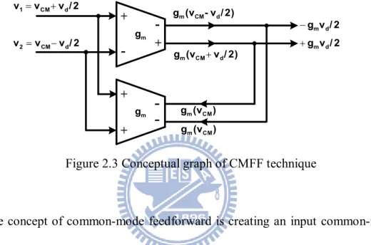
is its incapability to rejecting the common-mode signal which requires additional circuits to improve common-mode rejection ratio (CMRR). The CMRR is the ratio of the magnitude of the differential gain to the common-mode gain. An ideal differential amplifier has no common-mode gain and therefore has infinite CMRR. In this case, common-mode feedforward (CMFF) circuit is required which is shown in figure 2.3.
2 / v v v1 CM d 2 / v v v2 CM d m g m g 2) / v -(v gm CM d 2) / v (v gm CM d ) (v gm CM ) (v gm CM 2 / v gm d 2 / v gm d
Figure 2.3 Conceptual graph of CMFF technique
The concept of common-mode feedforward is creating an input common-mode signal through another signal path to output node. The common-mode signals can be canceled out and leave only differential signals at output node. In other words, it suppressed common-mode gain and leaves differential-gain to obtain high common-mode rejection ratio.
2.3 Linearity improving techniques
The purpose of the transconductor is ideally performing a linear conversion of input voltage to output current. Nevertheless, linearity has been an issue for all operational transconductance amplifiers especially the two conventional transconductor structures in the previous section since linearity in both circuits is
highly related to the transistor which is affected by process variation. In this section, five techniques for transconductor linearity enhancement are introduced.
2.3.1 Source Degeneration Differential Pair
Source degeneration structure is a widely used transconductor structure. The circuit is shown in figure 2.4. The main difference between source degeneration and original differential CMOS pair is the resistor connected between the sources of input transistors. The idea of this structure is to make signals from both input nodes go through transistor unchanged. The voltage drop over the resistor is thus the difference of two inputs; therefore the output current is generated from resistor and can be mirrored to output stage. Since the current is generated by resistor, it does not have non-ideal components from transistor like it does in other structures, thus leads to greater linearity performance.
1 V M1 M2 V2 1 V M1 M2 V2 R R R 2 B I 2 IB IB B I IB 1 O I IO2 1 O I IO2 VDD VDD B I IB (a) (b) Figure 2.4 Source degeneration schematics
However, there are still non-ideal terms in this structure. By analyzing transistors from small signal perspective, the equivalent input resistance between V1 and V2 is
not 2R. It has small signal resistance 2/gm1,2 between source node of transistor and
resistor. The actual total resistance is 2/gm1,2 + 2R. The term 2/gm1,2 can be ignored if
R is much larger than small signal resistance, therefore the nonlinear term 1/gm will
have minimal effect on the circuit. There are several ways to make the equivalent small signal resistance smaller to obtain higher linearity that will be discussed later this chapter.
The relationship of output current to the input voltage is shown as the following equation [1]:
id b , DS(sat) id o v N I K V N v -i 1 2 1 2 1 12 2 (2.7)and the overall transconductance of input cell is: N N R Gm 1 1 (2.8) where vid = V2 - V1, VDS(sat) = VGS(M1,M2) - Vtn and N = gm(1,2)R is the source
degeneration factor. By the equation (2.8), we can find the transconductance value is reduced by a factor of 1 + N. And the Taylor expansion of equation (2.7) can be derived and the third order harmonic term is shown as follow:
2 2 1 32 1 3 DS(sat) id V v N 1 HD (2.9)
In the equation (2.9), obviously, the HD3 of source degeneration pair degrades as the factor N becomes large. It means the circuit can reach high linearity by choosing large resistor R. However, the overall Gm will decrease as well.
In figure 2.4, two structures of source degeneration are presented, and both can be described by the same voltage to current transformation equation as in (2.7).
However, there some advantages and disadvantages for each circuit. In figure 2.4(a), the resistor requires a voltage drop, and then the range of the common-mode voltage is reduced, also the higher voltage supply is required. In figure 2.4(b), the noise of current source will appear at the output because two ways of current sources can generate unequal noise and feed to input transistor M1 and M2 separately. Otherwise
the mismatch of the current source would reflect as the input offset.
2.3.2 Triode Transistor Input Pair
All the input pairs described above are operating in saturation region. In this subsection, we will introduce the transconductor input pair with transistors working in the triode region. When the transistor works in triode region, the voltage restriction VDS < VGS – Vtn is satisfied. From the classical model equation for an n-channel
transistor operating in the triode region:
2 2 DS DS tn GS OX n D V -V -V V L W C μ I (2.10)To reduce even-order distortion products as almost all the practical continuous- time circuit, the differential structure is adopted. When the triode transistors arranged in differential type, we can derive that the output current and input voltage relation:
d DS OX n O O O V V L W C μ -I I I 1,2 1 2 (2.11)
1 V M1 M2 V2 1 O I IO2 B I IB C V C V
Figure 2.5 Constant drain-source voltage transconductor
the output current not only proportions to Vd but also VDS. Therefore, if we want to get
a linear voltage-current conversion, the drain-source voltage of the input transistors must keep constant. Figure 2.5 shows the circuit to implement the constant drain- source voltage transconductor with triode input pair M1 and M2. The virtual short
feature of the OPamp can force the drain-source voltage of M1 and M2 equal to VC,
and thus the transconductance value can be tuned by voltage VC as the equation
described.
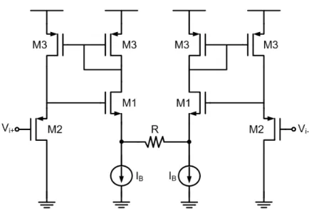
2.3.3 Flipped Voltage Followers
In this section, a basic cell for low-power or low voltage operation is introduced. Flipped voltage follower is one popular approach for low-voltage low-power circuit design, including the OTA design. The circuit is shown in figure 2.6 [12].
Figure 2.6 the Flipped Voltage Follower
The transistor M1 acts as a voltage follower which provides high input impedance while M2 forms a loop to create a low impedance node at the source of M1. Unlike the conventional voltage follower, the circuit is able to sink a large amount of current. However, the current source limits the sourcing capability. The large sinking capability is due to the low impedance at the output node. By analyzing the circuit, we can derive the output impedance ro = 1/gm1gm2ro1 approximately, where gmi and roi are
the transconductance and output resistance of transistor Mi, respectively.
2.3.4 Folded Flipped Voltage Followers
Another transconductor is shown in Fin. 2.7. This is another version of flipped voltage follower showed similar characteristics.
Figure 2.7 the Super Source Follower
The transistor M1 acts as a voltage follower which provides high input impedance while M2 forms a loop to create a low impedance node at the source of M1. The main behaviors are similar to flipped voltage follower. The major advantage of this structure over the original flipped voltage follower is that the input range is much larger, but at the cost of an extra current branch flows through M2. The properties of the super source follower are as follow. The output impedance of the super source follower is the same order as the flipped voltage follower, which is approximately ro = 1/gm1gm2ro1. Moreover, to acquire a correct operation point for the
transistors M1 and M2, the condition IB1>IB2 must be satisfied.
2.3.5 Source Degeneration Differential Pairs with Positive
Feedback
A transconductor with source-degenerated differential pair and a positive feedback gm-boosting circuit is shown in figure 2.8[13].
Figure 2.8 Source-degenerated Differential Pair with a Positive Feedback
The structure is based on the source degeneration differential pair and an extra boosting circuit. The main boosting circuit consists of transistors M2 and M3, with gm
of transistor M1 to be boosted. By choosing adequate M1 and M2 device dimensions, the positive feedback loop reduces the high source resistance to 50. The
approximate expression is as 2 1
1
1
m m sg
g
R
(2.12) where gmi is the transconductance of transistor Mi. This equation suggests the linearityChapter 3
Proposed Operational Transconductance Amplifiers
for High Linearity Applications
3.1 Introduction
An operational transconducance amplifier has the shortcoming of poor linearity. In the last chapter, several basic transconductor cells and methods for improving linearity are introduced. However, the overall linearity may not be sufficient for some applications.
With the advance of CMOS process technology, short-channel effects influence the performance seriously, especially in linearity. The voltage-current conversion no longer an ideal square function, more and more nonideal effects affect the circuits developed from this equation. Therefore, many compensation methods were proposed to improve linearity performance of a conventional transconductance circuit. Mobility compensation [10] uses a well-sized weak-inversion transistor to compensate for short-channel effect. Besides, two out-of-phase transconductors with unequal Gm
values can be combined to cancel out unwanted components of output signal [11]. However, the overall Gm may be reduced through this way.
two types of basic structure including pseudo-differential input and source- degeneration input in this chapter that achieved high linearity and suitable for many applications.
3.2 Proposed Operational Transconductance Amplifier with
Linearity Enhanced by Flipped Voltage Follower and Positive
Feedback
A linearity enhanced operational transconductance amplifier which combines the flipped voltage follower with positive feedback is proposed. The FVF structure has great characteristics for high linearity OTA design as mentioned in chapter 2. Moreover, positive feedback loop is implemented with FVF thus achieved better linearity.
3.2.1 Transconductor Gm stage
The proposed transconductor has two stages of operation. One of those is the Gm stage, and another one is programmable current mirror stage. Gm stage is introduced
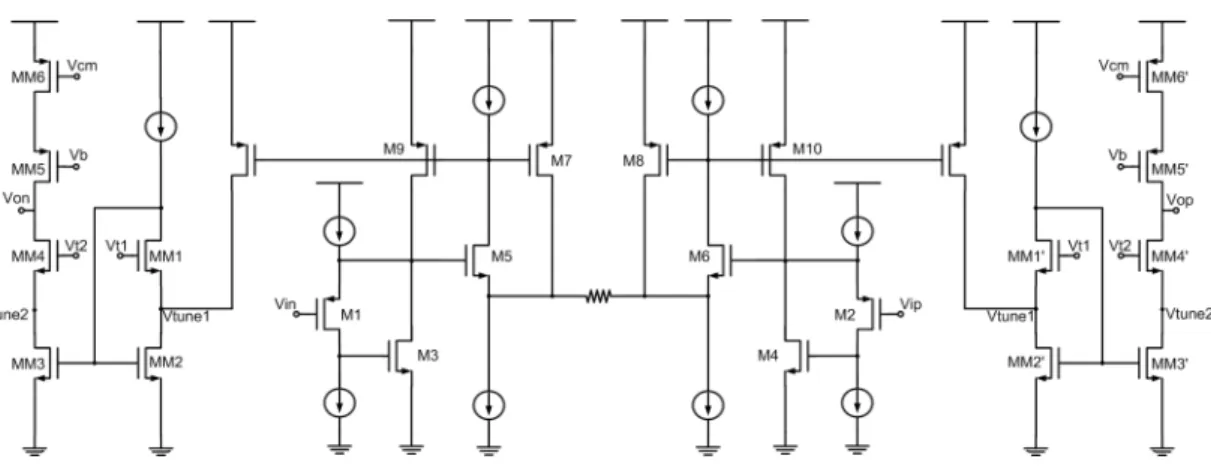
Figure 3.1 Transconductor Gm Stage
Transistors M1 to M4 and M5 to M8 are two pairs of folded flipped voltage follower. Negative feedback loops formed by these flipped voltage followers make the source of M1, M2, M5 and M6 became low impedance nodes. Moreover, with a same aspect ratio of M7 to M10, the positive feedback loops formed by M7 to M10 between voltage followers reduced the output impedance of nodes on both sides of resistor further more. The output impedance X and Y at source of M5 and M6 is given by 1 3 1 5 7 5 X
1
1
R
o m m o m mg
r
g
g
r
g
(3.1) 2 4 2 6 8 6 Y 1 1 R o m m o m m g r g g r g (3.2)This result is derived through several steps. At first, we transfer figure 3.1 into small signal model. And then, assuming the body effect is ignored for simplicity. Furthermore, the equations can be expressed by using the Kirchhoff's current law (KCL) and Kirchhoff's voltage law (KVL). Finally, the result is derived from these equations.
The value of RX could approximate to zero by choosing appropriate device size
for M1 to M8. By comparing the term with equation (2.12), the first and second terms of RX are quite less than RS. Therefore, the mismatch caused by process variation
could be minimized. From the equations (3.1) and (3.2), the transconductance can be presented as Y X total IN IP m
R
R
R
V
V
i
G
1
(3.3)where Rtotal is the sum of R1, R2 and Rtune. Minimizing the RX can suppress the
nonlinearity to acquire better total harmonic distortion (THD). As mentioned before, tuning the gate voltage of M25 can vary the transconductance.
Although this circuit is with many loops, stability of this circuit did not became an issue. The reason is that the output impedance and capacitance are larger than other nodes. As a result, the dominant pole is located at the output. Because the impedance and intrinsic capacitance of the other nodes are much lower than the output node, the second pole is in high frequency without affecting stability. The oscillation caused by positive feedback could be settled by larger common-mode feedback gain at cost of larger power consumption.
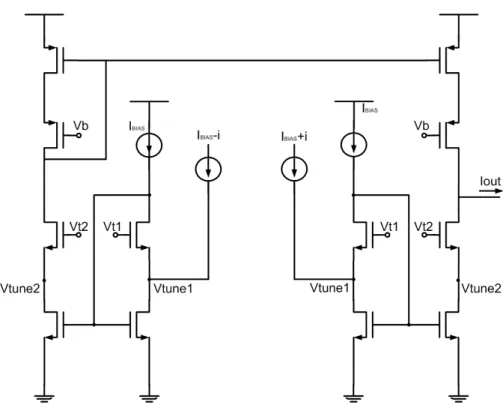
3.2.2 Programmable Current Mirror
Operational transconductance amplifier is an important building block of analog circuits. It is usually built with programmable characterics for versitile usage. Since the gm stage presented in previous section is lack of tuning mechanism. A current mirror with additional tuning ability is combined with the highly linear
transconductance stage in the previous subsection. This operational transconductance amplifier is introduced in this section [15] [16].
Figure 3.2 Programmable Current Mirror
The current mirror used transistors operating in triode region and external tuning voltage to achieve transconductance tuning. NMOS in this current mirror act as conventional low voltage cascode current mirrors. Bottom four transistors are the ones operate in triode region by controlling voltage Vt1 and Vt2 to make VDS less than VDSSat.
Current flow into this current mirror from main Gm stage is scaled also by controlling
voltage Vt1 and Vt2.
The equation for transistor working in triode region is:
DS DS TH GS D V V V V I 2 (3.4) where L W Cox n (3.5) If all the transistors are ideal, voltage equations Vtune1 = Vtune2 applies. Thus current
i I V V V V
I tune tune BIAS TH GS D 1 1 2 (3.6)
and current flow through transistor on the output side is
2 2 1 1 1 2 / 2 tune tune tune tune BIAS out D V V V V i I I I (3.7)
Total output current is substraction of two sides of whole circuit.
(3.8) Gm value for the whole circuits is able to be adjusted by tuning the ratio of both
of tuning voltages. The Gm of complete circuit is: R
V V V I tune tune d out 2 / g 1 2 m , R in this
equation is the resistor used in the main Gm stage. The conventional method of using
a MOS working in linear region to substitute for resistor provides a simple way to adjust transconductance. However, it suffers from the extra non-ideal effects generated from transistor used. These non-ideal terms affect parameters such as linearity, bandwidth, and gain, also makes the parameters vary with gm. The
programmable current mirror had been proposed to overcome this problem. It made that not to use transistor working in linear region possible which leads to higher linearity and fixed parameters such as bandwidth and gain.
3.2.3 Complete Transconductor Structure
A combination of previously mentioned gm stage and programmable current mirror made the complete transconductor structure.
in 1 2 2 2 1 out I tune Vtune V out I out I I
Figure 3.3 Complete Transconductor Structure
A highly linear operational transconductance amplifier is proposed. The new design makes use of the conventional source-degeneration structure, proposes a gm stage combines folded flipped voltage follower and positive feedback to improve linearity, and adds tuning functionality through a programmable current mirror while maintaining advantages of high linearity.
3.2.4 Common-Mode Feedback
In applications of Gm-C filter, the output of transconductor generally connects to
input of the next transconductor. One specific common-mode voltage is designed with the circuit. Consequently, a common-mode feedback circuit is required to maintain correct voltage at both input and output nodes of transconductor cells.
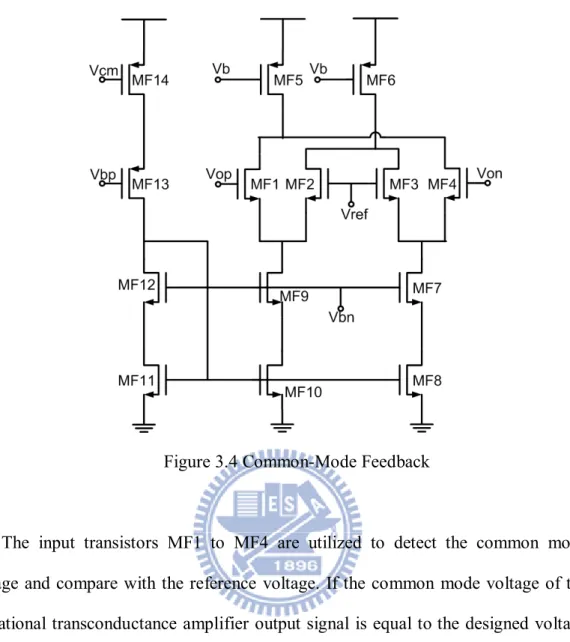
Figure 3.4 Common-Mode Feedback
The input transistors MF1 to MF4 are utilized to detect the common mode voltage and compare with the reference voltage. If the common mode voltage of the operational transconductance amplifier output signal is equal to the designed voltage VREF, the current through MF10 will keep constant thus the voltage VCM is fixed.
Nevertheless, the common mode of the operational transconductance amplifier output signal is not the same as VREF all the time. The voltage difference between them is
mirrored through MF10 to vary VCM, thus making the output common mode voltage
to the designed value. For example, if the output common mode voltages are larger than the VREF, the drain current of MF10 increases with it. The current mirror also
makes the current through MF11 increase, thereby VCM increased. In the output stage
of transconductor, increasing VCM leads to decrease of the output common mode
voltage. This mechanism of negative feedback loop makes the output common mode voltage equal to VREF.
When the operational transconductance amplifier operates at higher frequency, common-mode feedback circuit must be stable as well. The open loop gain of the common-mode feedback circuit is
L out
mf B mf A out mf mf out CMFB CMFB R sC g C s g C s R g R s g s A 1 1 1 ) ( ) ( 14 10 4 , 1 (3.9)where CA and CB are the total capacitance at the points of transistor 10 and
transistor 14, respectively. From the equation (3.9), the dominant pole is at )
/(
1 C L Rout and the non-dominant poles are at gmf10/CAandgmf14/CB. The non-dominant poles should be designed far away from the unit gain frequency to increase the phase margin of the operational transconductance amplifier.
3.2.5 Noise Analysis
Noise is another important aspect of the CMOS analysis. Several source of noise are influential in CMOS component. Thermal noise is due to the random motion of electron which is independent to the DC current flow. Flicker noise is also called “1/f noise” which has a spectral density inversely proportion to the frequency. For high speed circuit, the most significant noise source of a transistor is the thermal noise. For simpler derivation, the channel noise is modeled by a current source connected between the drain and source with a spectral density
η
δg kT
In2 4 m 1 (3.10) where k is the Boltzmann constant, T is absolute temperature, is device noise parameter which is dependent on the operation region of the transistor, gm is the small
depend on the bulk source voltage of transistor. By thermal noise model, the noise spectral density evaluated at the output node of proposed transconductor is derived as equation (3.11).
2 2 1 7 5 2 2 3 1 9 7 3 1 6 3 2 , 1 1 2 8 total mT m m total mm mm mm m m m m mm mm out n R R g g g R g g g g g g g g g kT I total
(3.11)where gmT1 is the transconductance of tail current transistors. From equation (3.11),
the source follower adds the input-referred noise whileproviding a voltage gain less than unity.The increase in degeneration factor, Rtotal, increases the noise contribution
of the tail current transistors since it is split in an unbalanced way causing differential output noise. Moreover, it can be the most significant noise component for large degeneration factors. Thermal noise can be reduced at cost of lowering transconductance.
3.3 Proposed Tunable Pseudo-Differential Transconductor
Linearity of the operational tranconductance amplifier is one of the most important arguments in recent research. It can seriously affect the performance of the circuit constructed by operational tranconductance amplifier such as Gm-C filters. As
described in previous section, a major non-linear term is approximately gm which is a
non-linear term that interferes the voltage to current conversion. Moreover, from experimental results of first chip, the linearity enhancement from flipped voltage follower is proven. The second chip makes use of it with another linearity enhancing technique: pseudo-differential structure and achieved better simulation result.
3.3.1 Modified Flipped Voltage Follower
To reduce non-linear terms generated from circuit, Folded Flipped Voltage Follower is introduced in chapter 2. This structure provides a low impedance node at source end of M1. The loop formed between transistor M1 and M2 makes impedance of the source node of M1 approximately 1/gm1gm2ro1, which is much smaller than
original 1/gm1. In this section, a modified version is proposed.
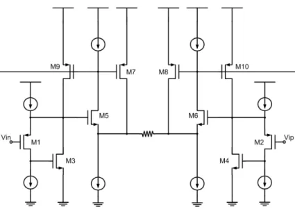
Figure 3.5 Modified Flipped Voltage Follower
A modified folded flipped voltage follower shown in figure 3 is proposed to maintain the merits of both pseudo-differential structure and flipped voltage follower. This modified circuit provides path to extract current to output from M1 to M4. The circuit has one extra single stage amplifier in signal path to make the gain higher which also makes equivalent impedance smaller
2 4 3 2 eq 1 r o m m m g g r g (3.12)
single stage amplifier is used in the signal path to make it possible to use NMOS as M4 which results in lower supply voltage requirement. Current through M1 also has to be larger than IB1 to maintain proper functionality. Meanwhile, the voltage
restriction at drain end of M4 is also reduced by one VGS from VGS+2VDS to 2VDS,
which makes the design of output node at the same stage possible.
The idea of this circuit is to make use of the small resistance at the source of M2. When connected to a triode region transistor which is equivalent to a resistor, the effects of resistance are minimized, thus obtain highly linear results.
The tuning voltage Vtune is to control the drain voltage of input transistor working
in triode region. Since the current flow through a triode region transistor is controlled by both drain voltage and gate voltage, controlling Vtune to alter the drain voltage is a
good way to achieve transconductance tuning.
3.3.2 Complete Transconductor Structure
The complete schematic is shown in figure 5. M1 to M14 make the main OTA Gm stage [16], [25]-[28]. M1 and M2 are the input pair. From small signal perspective,
we see the drain current is linear with respect to the applied drain-source voltage. Thus a small-signal resistance of
tn GS OX n V -V L W C μ DS
r
1 (3.13)As the input transistor working in linear region acts like a resistor, the resistance would be proportional to the gate bias voltage and transconductance tuning can be added by following circuits. M3 to M8 creates a low impedance node connecting to M1 and M2 also provides a current path to subtract and gain output current. The drain-source voltage of input transistor can be tuned by simply altering the gate voltage of M3. From the low impedance node it created a equivalent small signal resistance of 2 4 3 2 eq 1 r o m m m g g r g (3.14)
which effects the input transistor much less than the original pseudo-differential transconductor 1/gm1.
The req in series of input transistor is a major distortion term which can be
minimized by circuit proposed. The disadvantage of pseudo-differential transconductor is the sensitivity of the input common-mode voltage. Additional distortion terms are produced by common-mode signal since there is only one signal path for both common-mode signal and differential- mode signal. Therefore, M1’ to M14’ are to make the common-mode signal path to output node in order to cancel out common-mode small signal thus make CMRR higher which is required in
pseudo-differential structure. The two paths does not only make common-mode signal cancel out at the output nodes, also makes the voltage amplitude and current flow at output node twice as much with same gm value and at the same power consumption as other feedforward techniques.
3.3.3 Common-Mode Feedback Circuit
When using a fully-differential circuit, if the output stage bias current which is mirrored from the previous stage has a mismatch due to the fabrication variation, the output DC level will be directly affected. The key to solving this problem is to sense the increase or decrease of output voltage and form a negative feedback loop circuit to react against the variation. The common-mode feedback scheme will be able to
stabilize the common-mode output voltages of differential amplifier.
Figure 3.7 Common-Mode Feedback
The common-mode rejection ratio is generally worse on pseudo-differential structure than source degeneration ones due to the absence of tail current to control total current. Therefore an additional common-mode feedforward mechanism is
required otherwise transconductor will suffer from large common mode variation at output [17]-[19].
The extra circuit [24] to make output common mode voltage same as input common mode voltage is also required because when an OTA used as Gm of Gm-C
filter, the output voltage is also the input voltage of the next stage. The input common-mode voltage is designed in the beginning. Therefore if there is difference between output voltage and the input voltage of next stage, the circuit might not function properly.
The common-mode feedback circuit [20] used to maintain the output voltage at the designed value which is shown in figure 3.7. There are 2 sets of common-mode feedback circuit used on each side of the circuit due to different Vcm on each side. Its
currents are controlled by Vcm to make common-mode small signal flow through so
common mode signals are able to cancel out at the output node.
3.3.4 Noise Analysis
For high speed circuit, the most significant noise source of a transistor is the thermal noise. The noise model for the channel noise of transistor is introduced in subsection 3.2.5. The model is constructed by a current source connected between the drain and source with a spectral density
2 ' 13 13 3' 7' 5' ' 1 7 5 7 5 3 1 1 8 m m m m m sat m lin m m m m m sat m lin 2 n,out g g g g g δ g δ g g g g g δ g δ kT I (3.15)where sat andlinare noise parameters at saturation and linear region respectively. Thermal noise can be reduced at cost of lowering transconductance.
Chapter 4
Transconductance-C Filters
4.1 Introduction
Filters play a key role in virtually all sampled data systems. Most A/D converters are preceded by a filter which removes frequency components that are beyond the ADC's range. Some ADCs have filtering inherent in their topology. The most popular technique for realizing such an analog filter is a continuous-time filter, which can process high-speed signals continuously in time domain. There are three main techniques to implement an integrated continuous-time filter: active-RC filter, MOSFET-C filter and Gm-C filter. The active-RC filter is constructed by OP
amplifiers and passive elements resistors and capacitors. This filter structure provides good linearity and requires only designing a well performing OP amplifier. However, the resistors and capacitors it uses occupied enormous die area and significantly increased cost. The configuration of MOSFET-C filters replaces the resistors in an active-RC filter with the MOS transistors. Therefore, the resistance can be enhanced or depleted by applying an electrical field from a gate node. Nevertheless, the MOSFET-C filter generally has worse linearity due to the nonlinearity characteristics from the MOS transistors.
On the other hand, the Gm-C filter is formed by the capacitors and operational
transconductance amplifiers which are basic and important building blocks for various current-mode analog circuits and systems [1]-[3]. The transconductance-C filter has a better frequency response than the active-RC and MOSFET-C structures because of the open-loop operation and simple circuit structure of the transconductor. However, the performance of the transconductance-C filter highly depends on the transconductor building block, including the linearity and working speed. Therefore, most researches focus on the linearity improvement in the voltage-to-current conversion blocks of the filter [4]-[6].
For design of Gm-C filter [21]-[23], all types of filters such as Biquad
(second-order filter), Maximally flat magnitude filter, Chebyshev magnitude filter, Cauer filter, or LC ladder filter can be realized by Gm-C transconductance-capacitor
filter. This circuit is designed using Chebyshev magnitude filter structure. The advantage of using Chebyshev magnitude lowpass filter is the performance of Q value is good compare to other structures under the same order which means the transfer function has a sharper difference between passband and stopband. The Q value is worse than Cauer filter, the reason not using Cauer filter is that fully differential type of Cauer filter requires more capacitors. Single-end OTAs are usually used under Cauer filter structure which leads to lower chip area demand under signal path theory.
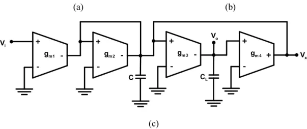
The OTA introduced in section above is now used as a building block of Gm-C
filter. Figure 6 showed a 4th-order Chebyshev lowpass filter built by gm blocks. Since all stages are with its own input and output nodes. A common-mode feedback circuit is indispensable to maintain dc voltages the same as designed value.
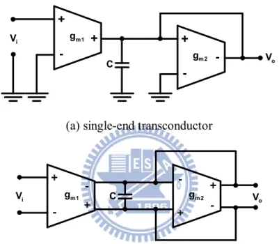
4.2 Elementary Building Blocks for Gm-C filters
The filter is composed of only gm block and passive capacitors so the specification of OTA is critical to the performance of filter. The linearity of gm block is also proportional to filter linearity. The design of active filter is developed from the passive filter, which is constructed by resistors, capacitors and inductors. And the active-RC filter is consisted of resistors, capacitors and integrators. Both passive and active-RC filter have developed detailed design process including transfer functions design and circuits level implementation. If we can construct elements have a same effective loading as passive elements, all the researches about passive and active filter can be transferred to the transconductor-C filter just by replacing the transconductor-based building blocks into original elements. The passband of filter cannot surpass the unit-gain frequency of gm block; moreover, the passband can be adjusted by transconductance tuning. This tuning mechanism can be used to overcome the process and temperature variation applied to filter thus made the cutoff frequency accurate. Elementary building blocks for a Gm-C filter [14] are introduced in the
following sections.
4.2.1 Resistors
There is generally little need for resistors in the area of Gm-C filters with the
exception of source and load resistors in doubly terminated LC ladders. However, the resistor is a necessary element in active and passive filter for low-sensitivity design. Thus we should develop a Gm-based resistor for the fundamental building block
before designing a Gm-C filter.
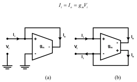
output terminal connected back to its positive input node. Since the transconductor input is ideally an open circuit, the input current Ii is equal to the transconductor
output current. Thus
i m o i I g V I (4.1) m g m g i V i I Io i V i I i I o I o I (a) (b)
Figure 4.1 Resistor simulations with transconductors (a) grounded; (b) differential
Consequently, the circuit's equivalent resistance value is
m o i i i g I V I V R 1 (4.2) Note that this is a grounded resistor becauseV is referenced to ground and the i inverse input node of transconductor is shorted to ground as well. For the differential usage, circuit is shown in figure 4.1(b). Notice that the feedback is negative as shown. A negative resistor with the resistance -1/gm would be created if positive feedback is
used. This differential type Gm-based resistor has a resistance value of
m o i i -g I V I -V V R 1 (4.3) as in figure 4.1(b), the negative feedback makes the input current equal to the output current then the resistance 1/gm is obtained. In addition, negative resistance could be
used to compensate transconductor losses or to eliminate inductor losses when very small but real spiral-wound inductors are used on ICs for filters at highest frequencies.