This content has been downloaded from IOPscience. Please scroll down to see the full text.
Download details:
IP Address: 140.113.38.11
This content was downloaded on 28/04/2014 at 11:16
Please note that terms and conditions apply.
Effects of High-Resistivity, Low-Temperature Layer in Transient Capacitance Measurements
of GaAs n-i-p Structures
View the table of contents for this issue, or go to the journal homepage for more 1998 Jpn. J. Appl. Phys. 37 L1238
(http://iopscience.iop.org/1347-4065/37/10B/L1238)
Jpn. J. Appl. Phys. Vol. 37 (1998) pp.L1238–L1240 Part 2, No. 10B, 15 October 1998
c
°1998 Publication Board, Japanese Journal of Applied Physics
Effects of High-Resistivity, Low-Temperature Layer in
Transient Capacitance Measurements of GaAs n-i-p Structures
Jenn Fang CHEN, Pai Yong WANGand Nie Chuan CHEN
Department of Electrophysics, National Chiao Tung University, Hsinchu, Taiwan, R.O.C.
(Received June 26, 1998; accepted for publication August 6, 1998)
Deep-level transient spectroscopy and transient capacitance measurements are performed on a molecular-beam-epitaxially grown GaAs n-i-p diode with a 2000- ˚A-thick low-temperature (LT)-grown layer immersed in its intrinsic region. The transient capacitance measurements reveal that the time constant and activation energy are the same for both the emission and capture processes. An equivalent circuit based on capacitance-frequency spectra is derived and used to obtain the resistivity values of the LT layer that are in agreement with experimental results. It is concluded that the transient capacitance observed corresponds to the resistance-capacitance time constant due to the LT-layer. In addition, the value of the activation energy is explained based on the equivalent circuit.
KEYWORDS: low-temperature GaAs, deep-level transient spectroscopy, transient capacitance, deep levels
L1238
Low-temperature (LT) grown GaAs has drawn much at-tention because of its high resistivity,1–3) relatively high
mobility4) and ultra short photo carrier lifetime.5, 6) A high concentration of AsGa defects1) or arsenic precipitates7) has
accounted for these properties. Among many different measurement techniques, deep-level transient spectroscopy (DLTS) is a useful technique for defect characterizations. Several groups have used it to study the defect levels in LT GaAs, but the observed values of activation energy and cap-ture cross section are usually not consistent with each other, partly due to the effect of the high-resistance LT layer, the properties of which are usually affected by growth parame-ters such as growth temperature, beam equivalent pressure, and annealing conditions. There exists a lack of understand-ing about the effects of the LT layer on deep-level character-izations. To illustrate this, we perform DLTS and transient capacitance measurements on a n-i-p diode with a LT layer immersed in the intrinsic region. The results are analyzed based on an equivalent circuit derived from the frequency-capacitance spectra in order to show the effects of the high-resistivity LT layer when interpreting the data.
The LT sample is a p-i-n GaAs diode, consisting of 1µm n(5 × 1017cm−3)/0.2 µm undoped LT/0.6 µm undoped/p(1017cm−3), grown on (001) n+-GaAs substrate
using a Varian Gen-II molecular beam epitaxy (MBE) sys-tem. The LT layer was grown at 300◦C. On top of the p layer, a heavily doped 0.5µm-thick p+(>5 × 1018cm−3) cap
layer was grown to facilitate a good ohmic contact. After the LT growth, the substrate temperature was raised to 600◦C for growth of the rest of the layers, thus the LT layer was sub-sequently annealed for about 1 hour. For comparison, a ref-erence sample with the same structure as that of the p-i-n LT sample, except that the 0.2µm undoped LT layer for the LT sample was also grown at the normal temperature of 600◦C, was subsequently grown. In other words, this reference sam-ple has a 0.8µm-thick i layer. Both the LT and the reference samples were grown under a beam equivalent pressure ratio of As4to Ga of about 10 and a growth rate of 1µm/h.
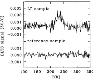
The DLTS spectra for the LT and reference samples are shown in Fig. 1. The measurements were performed at 500 kHz and carriers were injected by applying a forward bias of 0.3 V and then depleted at−3 V. It can be seen from Fig. 1 that there is no significant signal for the reference sample,
a similar activation energy of about Ea = 0.35 ± 0.02 eV,
indicating that both processes must overcome the same bar-rier. The activation energy was obtained by the slope of the temperature-corrected emission (capture) rateτ T2versus the
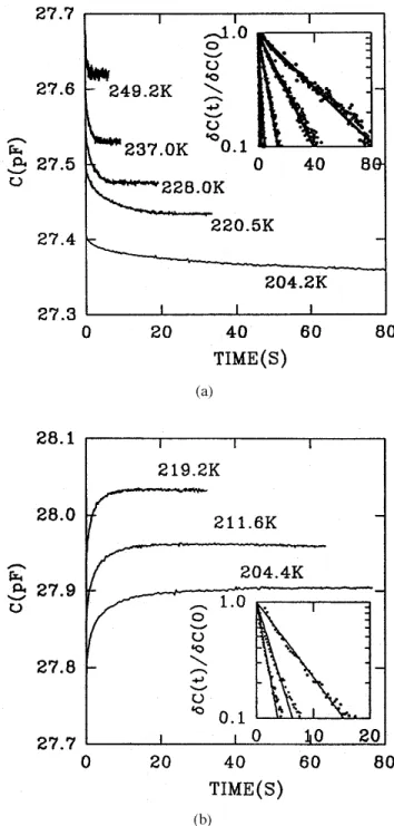
while a weak signal (1C/C ≈ 0.002) around 250 K is seen for the LT sample. Since the signal was not observed in the reference sample, it must be related to the LT layer. Due to the signal being weak, we were not able to determine the pa-rameters of the LT sample. Therefore, we directly recorded the emission response of the LT sample at 500 kHz, by first maintaining the sample at 0.2 V, and then changing to−2.5 V for the measurement. The result is shown in Fig. 2(a) along withδC(t)/δC(0) in the inset for a least square fit of its time constants. At the same time, we also recorded the capture response, by first maintaining the sample at−2.5 V and then changing to 0.2 V. The result is shown in Fig. 2(b) along with itsδC(t)/δC(0) in the inset.
Figure 2 illustrates the following features: (1) the sion process behaves as a minority carrier trap, (2) the emis-sion and capture transient responses have similar magnitudes, (3) the capture time constantτ is equal to the emission time constant, and (4) the emission and capture processes exhibit
Fig. 1. DLTS spectra of the LT and reference samples at a time constant of 0.9 s. The LT sample reveals a weak deep-level signal.
Jpn. J. Appl. Phys. Vol. 37 (1998) Pt. 2, No. 10B J. F. CHENet al. L1239
inverse temperature 1000/T .
Here, we examine three possible explanations for the above features. The first explanation is based on the value of Ea.
The LT GaAs is known to have a VGaGa vacancy, which was
reported at about 0.3 eV above the valence band by Fang and Look8)and Witt.9)Although the values reported by them are
similar, we consider this explanation unlikely because a nor-mal defect should not have a significant capture barrier. It is even unlikely that the emission barrier is the same as the capture barrier. Therefore, we rule out this possibility.
The second explanation is based on the fact that both the emission and capture processes have the similar barrier. In the As precipitate model, a Schottky depletion region was
be-lieved to surround the As precipitate7)in LT GaAs. This could
lead to both processes having the similar barrier. However, the Eavalue (=0.35 eV) is much lower than the typically
be-lieved barrier of 0.7–0.8 eV. Moreover, each As precipitate is likely to capture more than one electron. If the capture bar-rier is due to the electric field created by the already captured electrons, the barrier heightφBshould be proportional to the
number of captured electrons nt, that is qφB = αnt, whereα
is a proportional constant. Therefore, the time variation of nt
can be expressed as dnt
dt = σnvthn e
−qφB
K T = σnvthn e−αntK T,
whereαnis the capture cross section,vthis the thermal
veloc-ity and n is the free electron concentration, and nt(t) is solved
as nt(t) = K T α Ln µ t+ τ τ ¶ , where τ = K T ασnvthn .
From this equation, the number of electrons being captured by As precipitate depends on time, indicating that the capture transient should be a log function with a behavior similar to that observed for dislocation core10)instead of an exponential
function. However, this is contradictory to what is shown in Fig. 2. Therefore, we also rule out the explanation that the Schottky depletion model gives rise to the observed transient responses.
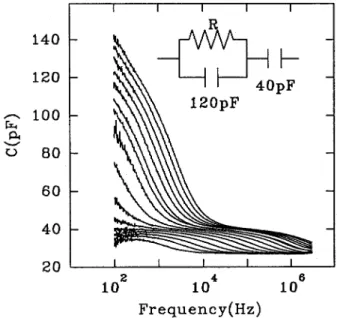
The third explanation come from the fact that the LT layer is highly resistive. This high-resistivity layer causes a resistance-capacitance (RC ) effect which is irrelevant to for-ward or reverse bias. This will result in the emission time constant being equal to the capture time constant. In order to verify this origin, we need to determine the equivalent circuit for the LT sample. Figure 3 shows the capacitance-frequency
C - f spectra measured for the LT sample. The spectra
demon-strate two C steps: the low-frequency step (from ≈120 to
≈40 pF) and the high-frequency step (from ≈40 to ≈30 pF).
The high-frequency step corresponds to the RC time constant due to the LT layer and can be represented by an equivalent circuit, as shown in Fig. 3. A detailed explanation of these
C - f spectra has been given elsewhere.11)The LT layer is rep-resented by a resistance R in parallel with a parallel-plate capacitor of C1 = Adε ∼= 120 pF with d being equal to the
thickness of the LT layer (0.2µm). This circuit is in series with a capacitor of C2 = Adε0 ∼= 40 pF with d0being equal to
the thickness of the intrinsic layer (0.6µm). This equivalent circuit has a high-frequency capacitance of
C1C2
C1+ C2 ∼ = 30 pF
with a time constant ofτ = R(C1 + C2). This equivalent
circuit should give rise to the observed emission and cap-ture transient responses. From the transient time constants observed in Fig. 2, usingτ = R(C1+ C2), values of R can be
obtained at various temperatures, as shown in Fig. 4 by hol-low squares for the emission transient and solid squares for the capture transient. We found that their values are consistent with those of LT resistance, previously determined from C -ω measurements.11) Moreover, we have previously studied the
Fig. 2. (a) Emission capacitance transient for the LT sample along with its
δC(t)/δC(0) in the inset. The transient shows a minority carrier trap with
an activation energy of 0.35 eV. (b) The corresponding capture capacitance transient. The time constant and activation energy are the same for both emission and capture processes.
L1240 Jpn. J. Appl. Phys. Vol. 37 (1998) Pt. 2, No. 10B J. F. CHENet al.
resistivity of the LT layer by measuring the current-voltage-temperature characteristics of n+-LT-n+ structures.3)The
re-sistance values shown in Fig. 4 are also in agreement with
those measured from n+-LT-n+ structures. This agreement supports the conclusion that the R(C1 + C2) time constant
due to the high-resistivity LT layer gives rise to the observed transient responses in DLTS and transient capacitance mea-surements and that the corresponding activation energy value observed is in agreement with that of the resistivity of the LT layer.
Here, we explain why a value of 0.35 eV was measured for the activation energy. Based on the current-voltage character-istics of the n+-LT-n+structures,3)the conductivity of the LT layer changes from a band conduction (Ea = 0.72 eV) to a
hopping conduction when T < 250 K. The hopping conduc-tion reduces the activaconduc-tion energy. Therefore, the Eavalue
depends on the temperature at which the transient response is observed, which in turn depends on the rate window used. Since the transient response was observed at T < 250 K the hopping conduction effect cannot be neglected. This explains why the activation energy value observed is 0.35 eV instead of about 0.7 eV.
Finally, we discuss why the emission transient behaved as a minority carrier trap in Fig. 2(a). The measurement was performed at 500 kHz; at this frequency the capacitance is the parallel capacitance of C1(120 pF) and C2(40 pF), as shown
in Fig. 3. Its variation with bias is
δC = δ C1C2 C1+ C2 = C22 (C1+ C2)2 δC1+ C2 1 (C1+ C2)2 δC2.
Figure 3 shows that the time constant of δC1 (the
low-frequency C step) is too large to follow the measuring signal at 500 kHz. Therefore, the first term in the above equation is neglected and the capacitance variation is dominated byδC2.
SinceδC2 decreases with increasing reverse bias, as shown
in Fig. 6 in ref. 11, the transient capacitance decreases in the emission process and exhibits a minority carrier trap.
This work was supported in part by the National Science Council of the Republic of China under contract No. NSC-87-2112-M-009-022.
1) D. C. Look, D. C. Walters, M. O. Manasreh, J. R. Sizelove, C. E. Stutz and K. R. Evans: Phys. Rev. B 42 (1990) 3578.
2) F. W. Smith, H. Q. Le, V. Diadiuk, M. A. Hollis, A. R. Calawa, S. Gupta, M. Frankell, D. R. Dykaar, G. A. Mourouu and T. Y. Hsiang: Appl. Phys. Lett. 54 (1989) 890.
3) J. F. Chen, N. C. Chen, S. Y. Chiu, P. Y. Wang, W. I. Lee and A. Chin: J. Appl. Phys. 79 (1996) 8488.
4) D. C. Look, G. D. Robinson, J. R. Sizelove and C. E. Stutz: Appl. Phys. Lett. 62 (1993) 3004.
5) K. A. Mclntosh, K. B. Nichols, S. Verghese and E. R. Brown: Appl. Phys. Lett. 70 (1997) 354.
6) S. Gupta, M. Y. Frankel, J. A. Valdmanis, J. F. Whitaker, G. A. Mourou, F. W. Smith and A. R. Calawa: Appl. Phys. Lett. 59 (1991) 3276. 7) A. C. Warren, J. M. Woodall, J. L. Freeouf, D. Grischkowsky, D. T.
Mclnturff, M. R. Melloch and N. Otsuka: Appl. Phys. Lett. 57 (1990) 1331.
8) Q. Fang and D. C. Look: Appl. Phys. Lett. 63 (1993) 219. 9) G. L. Witt: Mat. Sci. Eng. B 22 (1993) 9.
10) T. Wosinnski: J. Appl. Phys. 65 (1989) 1566.
11) N. C. Chen, P. Y. Wang and J. F. Chen: J. Appl. Phys. 83 (1998) 1403. Fig. 3. The capacitance-frequency spectra for the LT sample. The
temper-atures for each curve are 300.2, 310.8, 319.5, 329.8, 340.2, 350.0, 360.0, 370.0, 380.1, 385.3, 390.0, 395.3, 400.2, 405.0, 410.1, and 414.4 K from bottom to top. The spectra show two C steps with the emission rate of the high-frequency step (C= 40 to 30 pF) corresponding to the RC time constant due to the LT layer11)and is represented by an equivalent circuit.
Fig. 4. The resistivity values of the LT layer derived from the time constant of the high-frequency C step in Fig. 3 (shown as solid circles), which are in agreement with those directly measured from LT layers in n+-LT-n+ struc-tures.3)The resistivity values derived from the emission transient (the
hol-low squares) and from the capture transient (the solid squares) are shown to be consistent with the resistivity values of the LT layer.