IEEE TRANSACTIONS ON COMPONENTS, HYBRIDS, AND MANUFACTURING TECHNOLOGY, VOL. 13, NO. 2, JUNE 1990 267
Intermetallic Formation on the Fracture of Sn/Pb
Solder and Pd/Ag Conductor Interfaces
BI-SHIO CHIOU, K. C. LIU, JENQ-GONG DUH, AND P. SAMY PALANISAMY
Abstract - Intermetallic formation between thick film mixed bonded conductor and S n B h solder is investigated. Microstructural evolution of the interfacial morphology, elemental and phase distribution is probed with the aid of electron microscopy and X-ray diffraction. There exists mechanical interlocking between conductor and substrate. Penetration of a Bi element into the substrate is observed. A decrease in adhesion strength occurs when the sample is aged at 130°C for a long period of time. Microstructural analysis reveals the segregation of Pb-rich and Sn- rich phases in aged samples and formation of intermetallic compounds Pd3Sn2, PdzSn, Pd3Sn2, PdSn, AgsSn, and Ag3Sn. It is argued that conductor swelling caused by tin diffusion into the conductor film and volume change resulting from the intermetallic formation are major factors in the degradation of the peel strength.
I. INTRODUCTION
IN/LEAD solders are commonly used in the electronic
T
industry as interconnects and bonding pads for microcir- cuits. During the soldering operation and subsequent joint life, intermetallic compounds form and grow. The formation of the intermetallic compound may cause mechanical failure during thermal or power cycle [ 11-[4]. Microcircuit performance and lifetime are then degraded as these intermetallics grow. How- ever, kinetics of the intermetallic growth and the effect of the intermetallic compounds on the physical and mechanical properties of solder joints are not yet well understood.The purpose of this research is to study the effect of in- termetallic formation on the fracture of a 63/37 Sn/Pb solder and Pd/Ag thick film conductor. Palladium/silver-based con- ductors are probably the most commonly used inks in the technology thick film hybrid circuits. The commercial signif- icance of Sn/Pb solder and Pd/Ag conductor in the electronic industry requires a better understanding of this material sys- tem. The microstructural evolution of the interfacial morphol- ogy is probed with the aid of electron microscopy and X-ray diffraction.
11. EXPERIMENTAL PROCEDURE
A . Sample Preparation
Two commercial Dupont Pd/Ag conductor pastes, and a 63/37 Sn/Pb' solder are employed in this paper. The test pat-
Manuscript received May 12, 1989; revised September 12, 1989. B.-S. Chiou is with the Institute of Electronics, National Chiao Tung Uni-
K. C. Liu and J.-G. Duh are with the Department of Materials Science P. S. Palanisamy is with Delco Electronics, General Motor Corporation, IEEE Log Number 8932944.
'
Multicore Soldering Technology Ltd. versity, Hsinchu, Taiwan.and Engineering, National Tsing Hua University, Hsinchu, Taiwan. Kokomo, IN 46902.
0 lOcm
0 30cm
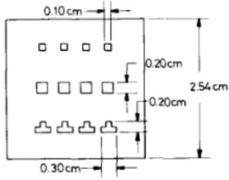
Fig. 1. Conductor test pattern employed in this study. tern, shown in Fig. 1, was printed on 96% A1203 substrate2 and dried at 150°C for 15 min. Samples were then air fired in a belt furnace. The total firing cycle time at 32 min with 7 min of peak firing at 850°C. Adhesion was evaluated by use of a wire/peel test. Four wires of 0.8-mm diameter were placed on every substrate crossing each pad. The wires were lined up with the three pattern features and the loop on the bottom edge. The loop was clipped after the soldering process. Test samples were then stored at 135°C for 0, 40, 100, 210, 400, and 600 h. Wires were bent 90" before the adhesion test. The adhesion strength was determined by pulling the wire us- ing an Instron machine with a strain rate of 26.2 mm/min or 2.28 mm/min. The fracture mode of the test specimens was examined.
B . Analysis and Characterization
Compositions of the conductors employed in this study were analyzed with an Atomic Emission Spectrometer (AES, GVM-lOOOP, Schimadzu, Japan) and an X-ray diffractometer (XRD, D/MAX-B, Rigaku, Japan). Microstructure and ele- mental distribution of the specimens were investigated with a scanning electron microscope (SEM, S250MK3, Cambridge, England) and an electron probe microanalyzer (EPMA, JCXA-733, JEOL, Japan). Oxidation state of some conductor constituents was identified with ESCA (Electron Spectroscopy for Chemical Analysis, Perkin-Elmer PHI 1905, Minnesota).
111. RESULTS AND DISCUSSION A . Characteristics of the Conductor
Two Dupont mixed bonded PdlAg conductors, designated as DC1 and DC2, are employed in this paper. The Pd/Ag ra- tios and the major constituents of these two conductors are identified by X-ray diffraction and AES, respectively. The cell constant, a, obtained from XRD experiments versus the
Nelson-Riley function, (cos2
e /
sin 8 +cos2e / O )
[ 5 ] , for two conductors are plotted in Figs. 2 and 3. The least square fitting*
AlSiMag 614, 3M Co. 0148-641 1/90/0600-0267$01 .OO0
1990 IEEE268 IEEE TRANSACTIONS ON COMPONENTS, HYBRIDS, AND MANUFACTURING TECHNOLOGY, VOL. 13, NO. 2, JUNE 1990
A NELSON -RILEY FUNCTION
407R
Cos%/sine + cosze/e
Fig. 2. Lattice parameter versus Nelson-Riley function for conductor DCl.
_ _ _ 25 K Ag ( 1 I1 ) 2. Lo a c e W(Il1) 8 36.60 3800 40 00 41 20
diffraction angle 28 (degree)
Fig. 4. X-ray diffraction pattern of conductor DC1.
4 021 I
diffraction angle 28 (degree)
Fig. 5 . X-ray diffraction pattern of conductor DC2.
(2) where 0 is the diffraction angle corresponding to a Cu target. The lattice paramFters, which :re the intercepts in Figs. 2 and 3, are 4.05 A and 4.01 A for conductors DC1 and DC2, respectively. Values of Pd:Ag ratios were determined as 1:8.09 and 1:2.33, respectively, for DC1 and DC2, on the basis of the associated correlation of the lattice parameter in Pd-Ag solid solution [6].
Pd:Ag ratios can also be determined from the ratio of the area under (111) peak in Figs. 4 and 5 of the X-ray pro- file. Pd:Ag ratios thus obtained are 1:7.5 for DC1 and 1:2.99 for DC2. AES results on the major constituents of DC1 and DC2 are summarized in Table I, which indicates that conduc- tor DC2 has higher Pd content than DC1 does. The average Pd:Ag ratio is 1:8 for DC1 and 1:3 for DC2. It appears that Pd: Ag ratios evaluated by three different methods are fairly comparable.
I I I I
0 1 2 3 4
Cos%/slne+ cOs2ele
Fig. 3. Lattice parameter versus Nelson-Riley function for conductor DC2.
of the two linear plots are
conductor DC1: a = 4.05
+
2.036 x($
+-)
cos2e
(1)e
(
cos2e
I cos2e )
e
conductor DC2: a = 4.01 - 0.00113 ~ sin 0Fig. 6. Cross-sectional SEM micrograph and X-ray mapping of as fired conductor DC2. (a) SEI. (b) Ag X-ray mapping. (c) Pd X-ray mapping. (d) Bi X-ray mapping.
TABLE I
AES RESULTS ON MAJOR CONSTITUENTS OF CONDUCTORS DCl A N D DC2
Pd Ag P b B i cu Pd:Ag
( R e l a t i v e C o n c e n t r a t i o n ) *
DC1 1 0 3 6 . 4 8 9 6 3 . 6 J 7 7 . 2 1 2 4 2 . 4 6 . 6 7 1 : 8 . 6 5
DC2 2 2 4 2 . 2 7 7 5 7 . 8 1 5 2 . 1 1 0 0 8 . 9 4 . 7 8 1 : 3 . 4 6 * N o r m a l i z e d t o Pd + Aq = 10000
CHIOU el al.: FRACTURE OF S n P b SOLDER AND PdiAg CONDUCTOR INTERFACES 269
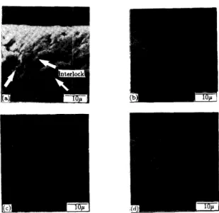
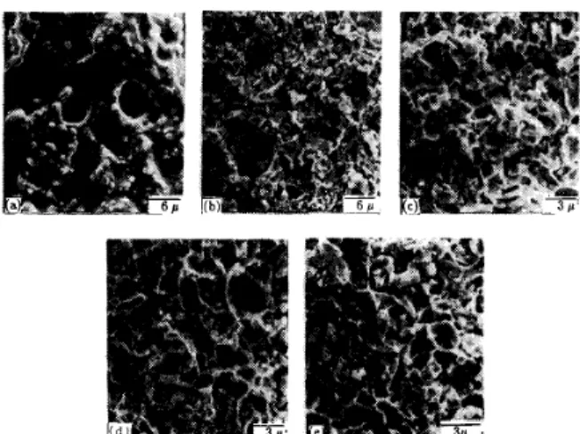
Fig. 7. Fracture surface of conductor DCl after various time of aging at 13OoC. (a) 0 h. (b) 40 h. (c) 100 h. (d) 210 h. (e) 400 h. Fracture occurs at the conductor/solder interface.
Thermal Storage at 130%
''1
Cross Head speed f 2 6 2 m m l m i n4
2 2 8 m l r n i nTABLE I1
FAILURE MODE OF CONOUCTORS AFTER PEEL TEST
2 0 0 ' I UK) 600 0 4 0 loo MO A g i n g Time ( h r ) (a) 10 0 LO loo MO
P - i m
0 A g i n g (b) Time ( h r )Peel strength as a function of aging time for conductor (a) DC1 and (b) DC2. C o n d u c t o r DC1 F r a c t u r e M o d e Aging S t r a i n A T i m e r a t e B C at 1 3 0 ' C ( h r ) mm/min 2 6 . 2 1 2 / 1 2 * 2 . 2 8 2 6 . 2 8 / 8 2 . 2 8 8 / 8 0 9 / 1 2 3 / 1 2 4 0 2 6 . 2 5 / 8 3 / 8 2 6 . 2 6 / 1 2 6 / 1 2 2 . 2 8 8 / 8 1 0 0 2 . 2 8 4 / 8 4 / 8 2 1 0 2 6 . 2 7 / 8 1 / 8 4 0 2 2 . 2 8 4 / 8 4 / 8 2 6 . 2 8 / 8 2 . 2 8 8 / 8 6 0 0 C o n d u c t o r DC2 F r a c t u r e M o d e Aging S t r a i n A T i m e at 1 3 0 ° C r a t e B C ( h r ) mm/min 0 40 26.2 8 / 8 2 . 2 8 8 / 8 2 6 . 2 8 / 8 2 . 2 8 6 / 8 2 / 8 2 6 . 2 6 / 8 2 / 0 2 . 2 8 2 / 8 3 / 8 3 / 8 1 0 0
cross-sectional SEM micrograph and X-ray mapping ^ . ^ 2 6 . 2 6 / 8 1 / 8 1 / 8
of the as-fired conductor DC2 is given in Fig. 6. Mechanical interlocking between the conductor and the substrate is ob- served at the conductor/substrate interface. Penetration of the Bi element into the substrate of the conductor/substrate inter- face is clearly observed, as shown in Fig. 6(d). This suggests the existence of chemical bonding between the conductor and the substrate.
SEM micrographs of the fracture surface of conductor DC 1 after 0-, 40-, 100-, 210-, and 400-h aging at 130°C are given in Fig. 7. For this specimen, fracture occurs at the solderkonductor interface. Dimple structure is observed after 40-h aging. The peel strength as a function of aging time for DCl and DC2 are given in Fig. 8. The peel strength decreases
with the aging time initially and then reaches an equilibrium value after 40-h aging for DC2 and after 100-h aging for DC1.
,~ ,~ 2 . 2 8 4;8 4/8 L I U 2 6 . 2 4 / 8 1 / 8 3 / 8 2 . 2 8 3 / 8 4 / 8 1 / 8 2 6 . 2 4/13 2 / 8 2 / 8 2.28 2 / 8 4 / 8 2 / 8 4 0 2 6 0 0 t h e v a l u e in t h e d e n o m i n a t o r i n d i c a t e t h e t o t a l number of test s a m p l e s , w h i l e t h a t in t h e n u m e r a t o r is t h e no. of s a m p l e s f a i l e d a s t h e s p e c i f i e d mode.
Strain rate does not seem to affect the peel strength of either conductor as indicated in Fig. 8.
B . Aging Behavior of Soldered Thick Film Joints Solder joint failure is classified into three modes. Mode A is defined as failure at the conductor/substrate interface. Mode B represents a solderkonductor interface failure, and mode C is a wireholder interface failure. Table I1 summarizes the fail-
270 IEEE TRANSACTIONS ON COMPONENTS. HYBRIDS, AND MANUFACTURING TECHNOLOGY, VOL. 13, NO. 2, JUNE 1990
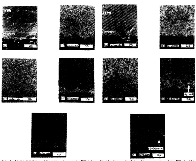
Fig. 9. Cross-sectional view of the sample with conductor D C l , before aging. (a) SEI picture. (b) Sn X-ray mapping. (c) Pb X-ray mapping. (d) Ag X-ray mapping. (e) Pd X-ray mapping.
ure mode of the conductors after the peel test. For specimens with conductor DC1, the majority of the failures occur at the solder/conductor interface (mode B ) when aging time is less than 40 h. Mode A failure is found for samples aged from 100
to 400 h. However, for specimens with conductor DC2, frac- ture occurs mostly at the conductor/substrate interface (mode A ) . For samples aged longer than 40 h, some specimens have a mode B failure.
The cross-sectional SEM micrographs and X-ray mapping of the soldered specimens before aging and after aging at 130°C for different times are given in Figs. 9 and 10 for con- ductors DC1 and in Figs. 11-13 for conductor DC2, respec- tively. Microstructural changes are observed in solder materi- als after 100-h aging at 130°C. As shown in Figs. 10, 12, and 13, segregation of both Sn-rich and Pb-rich phases occurs as the samples are aged for longer than 100 h. Tin is found in conductor/substrate interface after 100-h aging for conductor DC1 and after 40-h aging for conductor DC2. The 100-h ag- ing time corresponds to the minimum peel strength of samples
with conductor DC1, as shown in Fig. 8(a). C . Adhesion Loss Mechanism
On a system containing a frit-bonded conductor screen printed on a dielectric substrate, Milgram [7] reported that the tin from the Sn/Pb solder replaced the silver at the silver-glass
Fig. 10. Cross-sectional view of the sample with conductor DC1 after 100- h aging. (a) SEI picture. (b) Sn X-ray mapping. (c) Pb X-ray mapping. (d) Ag X-ray mapping. ( e ) Pd X-ray mapping.
interface and degraded the peel strength. Taylor et al. 181 ar-
gued that the tin metal from the solder diffused along grain boundaries of the metal and reduced bismuth oxide to bis- muth metal. Degradation in adhesion is most severe when the layer of bismuth oxide, i.e., the chemical binder, at the substrate/conductor interface is destroyed. Loasby et al. [9] suggests that the volume change caused by tin diffusion into the conductor film and subsequent intermetallic formation de- grades the adhesion strength. The X-ray diffraction patterns of 100-h aged samples with conductor DC1, shown in Fig. 14, reveal the existence of alloys AgsSn, AgsSn, Pd3Sn, PdsSnz, PdSn, and Pd2Sn. Fig. 15 gives the X-ray diffraction results of samples with conductor DC2 after 0- 40-, and 210-h thermal aging at 130°C. The XRD data suggests the coexistence of PdsSn, PdzSn, PdsSn2, PdSn, AgsSn, and Ag3Sn. The crys- tal structure, lattice parameter, and unit cell volume of the Pd-Sn and Ag-Sn alloys 1101-1131 are summarized in Table 111. The lattice parameter and qnit cell volume of conductor DC1 and 4.051
A
and 66.48 A , respectively.Conductor/substrate solderkonductor interface failures and minimum peel strength occur when DCl samples are aged for 100 h and DC2 samples aged for 40 h, as indicated
CHIOU et al.: FRACTURE OF SniPb SOLDER AND PdiAg CONDUCTOR INTERFACES 27 1
Fig. 11. Cross-sectional view of the sample with conductor DC2 before aging. (a) SEI picture. (b) Sn X-ray mapping. (c) Pb X-ray mapping. (d) Ag X-ray mapping. (e) Pd X-ray mapping.
in Table 11. Segregation of tin-rich and Pb-rich phases be- comes severe, as shown in Figs. 10 and 12. Hence, conduc- tor swelling caused by tin diffusion into the conductor film and volume change caused by subsequent intermetallic forma- tion of AgsSn, AgsSn, Pd3Sn, PdSn, PdzSn, and Pd3Sn2 are the major reasons for the loss of adhesion strength for both conductors.
The oxidation state of the Bi element on the fracture sur- faces of the unaged and 40-h aged DC2 samples is investigated by Auger electron spectroscopy. The ESCA results, shown in Figs. 16 and 17, reveal a 4f5/2 electronic structure of the Bi element. This suggests that Bi element exists in oxide form, Bi203 [14], [15], instead of metallic form, Bi. This implies that reduction of BiZ03 is not the major cause for the de- gration of adhesion strength in systems containing conductor DC2.
The room temperature resistivities of elements Pb, Pd, Ag, and Sn are 20.65 p f l . cm, 10.8 p 0 . cm, 1.59 pi2
.
cm, and 1 1.10 p f l.
cm, respectively [ 161. Due to the defect scattering of charge carriers, alloys such as Ag3Sn, PdzSn, etc, haveFig. 12. Cross-sectional view of the sample with conductor DC2 after 40-h aging. (a) SEI picture. (b) Sn X-ray mapping. (c) Pb X-ray mapping. (d) Ag X-ray mapping. (e) Pd X-ray mapping.
larger resistivities compared to the constituent components, Ag, Pd, and Sn [17]. The formation of the Pb-rich layer is observed on top of the conductor for DC1 after 100-h aging, shown in Fig. 10(d), and for DC2 after 400-h aging, shown in Fig. 13(c). The larger resistivities of the formed alloy and the Pb-rich layer increase the electrical resistance of the solder joint after aging. The enhanced resistive heating raises the temperature at the solder joint and consequently accelerates the degradation of the solder joints during application.
IV. SUMMARY AND CONCLUSIONS
1) Intermetallic formation between thick film mixed bonded conductor and Sn/Pb solder is evaluated. The conductor pastes in this study have a Pd: Ag ratios of 1 :8 and 1 : 3 for DC 1 and DC2, respectively.
2) Microstructural analysis of the soldered conduc- torhbstrate assembly reveals the existence of mechanical in- terlocking between conductor and substrate, as well as the penetration of Bi element into the substrate side of the con- ductorhbstrate interface.
272 IEEE TRANSACTIONS ON COMPONENTS, HYBRIDS, AND MANUFACTURING TECHNOLOGY, VOL. 13, NO. 2, JUNE 1990
Fig. 13. Cross-sectional view of the sample with conductor DC2 after 400- h aging. (a) SEI picture. (b) Sn X-ray mapping. (c) Pb X-ray mapping. (d) Ag X-ray mapping. (e) Pd X-ray mapping.
1
1 I I I
30 40 60 80
Diffractlon angle 28
Fig. 14. X-ray diffraction pattern of the sample with conductor DC1 after 100-h aging. 30 40 60 m i Diffraction angle 28 (a) Diffraction Angle 28 (b)
1
1 I I I 30 40 60 80 85 Diffraction Angle 28 (C) 0 h; (b) 40 h; ( c ) 210 h; aging.Fig. 15. X-ray diffraction pattern of a sample with conductor DC2 after (a)
3) The decrease in adhesion strength occurs when samples
are aged at 130°C for longer than 40 h for DC2 or for longer than 100 h for DC 1. Investigation of the microstructure of the Sn/Pb alloy by SEM and EPMA reveals the segregation of Pb-rich and Sn-rich phases in the aged samples. X-ray diffrac- tion results suggest the formation of intermetallic compounds Pd3Sn2, PdZSn, Pd3Sn, PdSn, Ag5Sn, and Ag3Sn.
4) Conductor swelling caused by tin diffusion into the con- ductor film and voltage change caused by the intermetallic formation are the major reasons for the degradation of the
CHlOU et al.: FRACTURE OF SnPb SOLDER AND PdiAg CONDUCTOR INTERFACES 213
w l
TABLE 111
CRYSTAL STRUCTURE, LATTICE PARAMETER, A N D UNIT CELL VOLUME OF SOME Pd-Sn A N D Ag-Sn ALLOYS
Alloy Crystal Structure Lattice Parameter Unit Cell Volume
Ag3Sn orthorhombic .a = 2.995 A 73.87
i3
bo = 5.159 A c = 4.781 A Ag5Sn hexagonal .a = 2.966 A 34.63i3
co = 4.782 A Pd Sn orthorhombic .a = 8.11 A 194.42i3
bo = 5.662 A c = 4.234 A Pd3Sn2 hexagonal .a = 1.39 A 94.38 i 3 co = 5.655 APdjSn face center cubic a. = 3.97 A 62.57 i3
PdSn orthorhombic a. = 3.86 A 149.06
i3
bo = 6.12 Ac o = 6.31 A
i
A
peel strength. The reduction of Bi203 into Bi element is not a major cause in the decrease of the adhesion strength.
5) The high resistivity alloys as well as the Pb-rich layer on top of the conductor may accelerate the degradation of the solder joints.
ACKNOWLEDGMENT
B. S . Chiou appreciates the support and friendship from the Delco Group, General Motor Corporation.
0 W REFERENCES
170 166 162 158 154 [l] G. D. O’clock Jr., M. S. Peters, J. R. Patter, G. A. Kleese, and R. V. Martini, “Pb-Sn microstructure: Potential reliability indicator for
BINDING ENERGY . EV
Fig. 16. Multiple scan of Bi in ESCA spectrum for unaged DC2 sample. The major peak at 164.8 corresponds to a 4f512 electronic structure of Bi.
interconnects,” ZEEE Trans. Comp., Hybrids, Ma&. Technol., vol. CHMT-10, pp. 82-88, Mar. 1987.
P. W. Dehaven, “The reaction kinetics of liauid 60/40 S n P b solder 121
_ _
with copper and nickel: A high temperature X-ray diffraction study,” i n M a t . Res. Soc. Symp. Proc., vol. 40, 1985, pp. 123-128. D. S. Dum, T. F. Marinis, W. M. Sherry, and C. J. Williams, “De- pendence of Cu/Sn and Cu/6OSn4OPb solder joint strength on diffusion controlled growth of Cu3Sn and CusSns,” in Mat. Res. Soc. Symp. Proc., vol. 40, 1985, pp. 129-138.
[4] C. W. Allen, M. R. Fulcher, A. S. Rai, G . A. Sargent, and nickel-Tin interfacial zones,” in Mat. Res. Soc. Symp. Proc., vol.
. -
[5] B. D. Cullity, Elements of X-ray Diffraction, 2nd ed. Reading,-
w
I. Karakaya and W. T. Thompson, Bull. Alloy Phase Diagram, vol. 9 , no. 3, p. 23, 1988.
A. A. Milgram, “Influence of metallic diffusion on the adhesion of screen printed silver films,” Metallurgical Trans., vol. 1, pp. B. E. Taylor, J. J. Felten, and J. R. Larry, “Progress in and technol- 176 170 16L 158 ogy of low-cost silver containing thick film conductors,” ZEEE Trans.
Comp., Hybrids, Manuf. Technol., vol. CHMT-3, pp. 504-517, 1980.
6 - [3]
6 - A. E. Miller, “A study of intermetallic compound development in
W 40, 1985, pp. 139-144.
-
MA: Addison-Wesley, 1978, p. 356. z [6] [7] 695-700, 1970. [8] BINDING ENERGY , EV274 IEEE TRANSACTIONS ON COMPONENTS, HYBRIDS, AND MANUFACTURING TECHNOLOGY, VOL. 13, NO. 2, JUNE 1990 [9] R. G. Loasby, N. Davey, and H. Barlow, “Enhanced property thick-
film conductor pastes,” Solid-state Technol., pp. 46-50, 1972. [IO] I. R. Harris and M. Cordey-Hayes, “A study of some palladium-tin,
silver-tin and palladium-silver-tin alloy,” J . Less-Common Metals, H. W. King and T. B. Massalski, “Lattice spacing relationships and the electronic structure of the H.C.P. { phases based on silver,” Philosoph. Mag., pp. 669-682, 1960.
[ 121 0. Nial, A. Almin, and A. Westgren, “Ronttgenanalyse der Systeme Gold-Antimon und Silber-Zinn,” Z. Phuikal. Chem., vol. 138, pp. M. Hanson and K. Anderko, eds., Constitution of Binary Alloys, vol. 16, pp. 223-232, 1968.
[Ill
81-90, 1931. [I31
New York: McGraw-Hill, 1958; 1st Supplement, R. P. Elliott, Ed. New York: McGraw-Hill, 1965.
T. P. Debies and J. W. Rabalais, “X-ray photoelectron spectra and electronic structure of BiZX3 (x = 0, S, Se, Te),” Chem. Phys., vol. W. E. Morgan, W. J. Stec, and J. R. Van Wazer, “Inter-orbital binding-energy shifts of antimony and bismuth compounds,” Inorgan. Chem., vol. 12, no. 2, pp. 953-955, 1973.
CRCHandbook of Chemistry and Physics, R. C . Weast, Ed. Boca Raton, FL: CRC, 1980.
R. W. Berry, P. M. Hall, and M. T. Harris, Thin Film Technology, New York: Van Nostrand Reinhold, 1982, pp. 303-307.
[14]
20, pp. 277-283, 1977. [15]
(161 [17]