MULTILEVEL ROUTING WITH ANTENNA AVOIDANCE
防止天線效應之多階繞線器
摘 要 隨著製程技術進步到奈米境界,天線效應已對繞線問 題上造成很大的影響。天線效應是指導體上充電累積對閘 極造成退化的現象。特別在使用高密度離子的深次微米技 術下,天線效應會直接影響電路的可製造度及良率。除此 之外,持續增長的電路繞線複雜度也對既存的繞線演算法 造成極大的影響。在這篇論文裡,我們提出了一使用自建 跳線機制來防止繞線天線問題之創新多階繞線架構。實驗 結果指出,我們的方法可順利防止所有閘極上所產生的天 線效應問題。 關鍵詞:實體設計、繞線、多階最佳化、天線效應、可製 造度設計。Abstract
As technology advances into nanometer territory, the antenna problem has caused significant impact on routing tools. The antenna effect is a phenomenon of plasma- induced gate oxide degradation caused by charge accumulation on conductors. It directly influences reliability, manufacturability and yield of VLSI circuits, especially in deep-submicron technology using high density plasma. Furthermore, the continuous increase of the problem size of IC routing is also a great challenge to existing routing algorithms. In this paper, we propose a novel framework for multilevel full-chip routing with antenna avoidance using built-in jumper insertion approach. Compared with the state-of-the-art multilevel routing, the experimental results show that our approach reduced 100% antenna-violated gates and results in fewer wirelength, vias, and delay increase.
Keywords: Physical design, routing, multilevel
optimization, process antenna effect, design for manufacturability (DFM).
1. INTRODUCTION
With the continuous and rapid increase in complexity of VLSI designs and fabrication technologies, manufacturing yield and product reliability are now among the most important design issues, such as quick turn-around time, small die size, high speed, low power, and so on [6]. The fine feature size of modern IC technologies is typically achieved by using plasma-based processes. As the technology enters the deep-submicron era, more stringent process requirements cause some advanced high-density plasma
reactors adopted in the production lines to achieve fine-line patterns [11]. However, these plasma-based processes have a tendency to charge conducting components of a fabricated structure. The existing experimental evidence indicates that charging may affect the quality of the thin oxide. This is called the antenna effect (also called “plasma-induced gate oxide damage”). During metallization, chips are usually processed “from the bulk up”, each time adding an additional layer of interconnect. While the metal interconnect chip is being assembled, the interconnect of a net will consist of a number of disconnected pieces of floating metal. Long floating interconnects act as
Tsung-Yi Ho* Yao-Wen Chang** Sao-Jie Chen**
何 宗 易
張 耀 文
陳 少 傑
*
Ph.D. student **Professor Graduate Institute of Electronics Engineering, National Taiwan University, Taipei, Taiwan 10617, R.O.C.
*
博士班研究生 **教授 國立臺灣大學電子工程學研究所
temporary capacitors to store charges gained from the energy provided during fabrication steps such as chemical mechanical polishing (CMP). A random discharge of the floating node due to subsequent process steps could permanently damage transistors, rendering the IC useless [9,17,20]. For example, the exposed polysilicon and metal structures connected to a thin oxide transistor will collect charge from the processing environment (e.g., reactive ion etch) and damage the transistor when the discharging current flows through the thin oxide.
Although the mechanism of the gate oxide damage is not very well understood, the precise experimental relationships between the amount of damage and the antennas have been studied [17,20]. Since the plasma damage is caused by the electrical charging of devices during plasma processes, the damage increases with an increase in the area of the exposed conductor (antenna) during the plasma process. In order to reduce or prevent damage to the gate oxide from the plasma process, and thus to ensure reliability of a chip, a circuit layout rule that considers the antenna effect (antenna rule) is employed. The conventional antenna rule restricts a maximum antenna size or antenna ratio allowed for circuit layout. Recent studies show that the damage, considering all plasma-based manufacturing operations, increases in proportion to both the area and the perimeter of the antennas [18]. A more accurate model considering the cumulative oxide damage is discussed in [1]. These models provide a good guideline for routers or physical EDA tools to help reduce damage from the antenna effect and get higher yield and reliability.
Maly et al. [14] proposed a method for detecting an antenna violation. He calculated both the area and the perimeter of antennas using a general-purpose design rule checking (DRC) program. However, the method does not indicate any measures to feed the antenna information back to a layout generation. On the other hand, Wang et al. [19] proposed a channel router which considers the antenna effect. They introduced a layer restriction to a conventional channel router, which limits the maximum length of the wires with antenna problems. Chen and Koren [2] also proposed a network bipartitioning approach for layer restriction. But both of them consider antenna effect minimization only in 3-layer channel routing. Shirota et al. [18] proposed a router which combines a traditional router with a modification of wires for reducing the antenna effect damage, using a rip-up and reroute method. But this method fixes the antenna after routing; it is not a built-in approach. The diode insertion method is also proposed to fix the antenna problem [2,8]. It is the simplest way to deal with antenna problems by forcing a discharge
path. But in today’s high-density VLSI layouts, there is simply not enough room for “under-the-wire” diode insertion for all wires. Furthermore, it will cause congestion, add capacitance to the net, reduce room for ECO, and generate leakage power. Thus, people often prefer a jumper-based solution to a diode-based solution for more advanced process technology.
Routing complexity is also an important problem for modern routers. To cope with the increasing complexity, researchers have proposed multilevel approaches to handle the problem [3,4,7,13]. The multilevel framework has attracted much attention in the literature recently [5]. It employs a two-stage technique: coarsening followed by uncoarsening. The coarsening stage iteratively groups a set of circuit components (e.g., circuit nodes, cells, modules, routing tiles, etc.) based on a predefined cost metric, until the number of components being considered falls below a certain threshold. Then, the uncoarsening stage iteratively ungroups a set of previously clustered circuit components and refines the solution by using a combinatorial optimization technique (e.g., simulated annealing, local refinement, etc). The multilevel framework has been successfully applied to partitioning, floorplanning, placement and routing in VLSI physical design.
In this paper, we propose a multilevel router for reducing the antenna effect damage by built-in jumper insertion. The three main features of the proposed method are: (1) a bottom-up approach is used for jumper prediction; (2) a state-of-the-art multilevel routing framework [7] is adopted for run-time speedup and antenna fixing; (3) nets that failed to route or violate antenna rule are routed at the uncoarsening stage for better routing completion. Experimental results show that our algorithm is very efficient.
The rest of this paper is organized as follows. Section 2 describes the antenna effect damage. Section 3 presents our multilevel framework for reducing antenna effect damage. Experimental results are shown in Section 4. Finally, we give concluding remarks in Section 5, as well as our goals for future work.
2. ANTENNA EFFECT DAMAGE
The mechanism of antenna damage is not fully understood, but there is experimental evidence indicating when charging occurs and how it may affect the quality of gate oxide [17,20]. Charging occurs when conductor layers not covered by a shielding layer of oxide are directly exposed to plasma. The amount of such charging is proportional to this plasma-exposed
area. If the charged conductor layers are connected only to the gate oxide, Fowler-Nordheim (F-N) tunneling current will discharge through the thin oxide and cause damage to it.
Process antenna rules adhere to the design requirement that the total charge accumulated on metal connected to a polysilicon gate during any stage of metalization cannot exceed a certain threshold, beyond which the excessive charge accumulation may permanently damage the gate. Let gate-strength (g,L) be the maximum length of a wire of minimum width on layer L that can be directly connected to the gate g without causing an antenna violation. The larger the values of gate-strength, the easier it is to fix the antenna violation. In 0.18-micron technology and above, gate-strength of 1000 microns and above is not uncommon, and fixing by post-processing suffices. In 0.13-micron and below technology, however, the average and worst-case gate-strength’s are substantially reduced (about 20 ~ 100 microns [12,15]). This is due in part to the use of cells with small gate areas (for example, extensive use of low-power cells) and a tightening of the antenna ratio. When the worst-case gate-strength is merely a handful of cellrows, antenna fixing becomes very challenging.
On the other hand, if the amount of charging collected by connected conductor layer patterns could be released through a low impedance path, such as a previously formed diffusion layer pattern (e.g., source/drain), it will not introduce the gate oxide damage.
A more accurate analysis of the cause of the charging collected during the deep submicron VLSI manufacturing operations shows that the perimeter length of conductor layer patterns must also be included in the calculation [18]. There are three types of plasma-based manufacturing processes:
1. Conductor layer pattern etching processes: The amount of accumulated charge is proportional to the perimeter length of conductor layer patterns. Etching processes divide conductor layer plates into innumerable routing patterns. In the late stage of the processes, the perimeters of the routings are directly exposed to plasma.
2. Ashing processes: The amount of accumulated charge is proportional to the area of the conductor layer patterns. Ashing processes remove remaining photo resist layers after etching processes of a conductor layer. In the late stage of the processes, the area of a conductor layer pattern is directly exposed to plasma.
3. Contact etching processes: The amount of
accumulated charge is proportional to the total area
of the contacts. Contact etching processes dig holes between two conductor layers. In the late stage of the processes, the area of all the contacts on the lower conductor layer pattern is directly exposed to plasma.
As a result, considering all the plasma-based processes, the risk of gate-oxide damage is proportional to the area and perimeter length of antenna routings and inversely proportional to the area and perimeter length of the gate oxide.
There are three kinds of solutions to reduce the antenna effect [1]:
1. Jumper insertion: Break only signal wires with antenna violation and route to the highest level by jumper insertion. This reduces the charge amount for violated nets during manufacturing.
2. Embedded protection diode: Add protection diodes on every input port for every standard cell. Since these diodes are embedded and fixed, they consume unnecessary area when there is no violation at the connecting wire.
3. Diode inserting after placement and routing: Fix those wires with antenna violations that have enough room for “under-the-wire” diode insertion. During wafer manufacturing, all the inserted diodes are floating (or ground). One diode can be used to protect all input ports that are connected to the same output ports. But this approach works only if there is enough room for diode insertion.
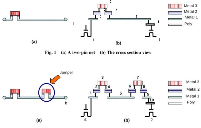
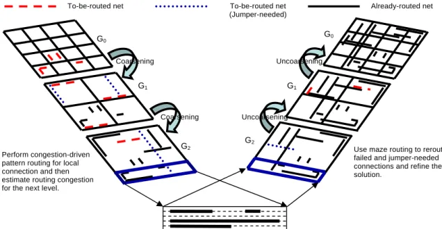
Jumper insertion is the most popular way to solve the antenna problem. Let us show its usage in the following example. Suppose we have a two-terminal net in which a is the source node and b is the terminal node (see Figs. 1(a) and 1(b)). In this case, the approximated gate-strength of b is the sum of the length of segments 4, 5, and 6, which may violate the minimum allowable gate-strength. If we add a jumper at the long segment 5 (see Figs. 2(a) and 2(b)), the approximate gate-strength of b is just the sum of the length of segments 8, 9, and 10, which will not violate the minimum allowable gate-strength. Thus, if we add jumpers appropriately, the antenna problem can be easily solved.
3. MULTILEVEL ROUTING
FRAMEWORK
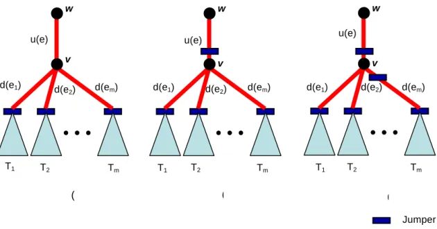
Our multilevel routing algorithm is inspired by the work of [7]. As illustrated in Fig. 3, G0 corresponds to
the routing graph of the level 0 of the multilevel coarsening stage. Before the coarsening process, we firstperformtheoptimaljumperpredictionforeverynet.
Fig. 1 (a) A two-pin net (b) The cross section view
Fig. 2 (a) A two-pin net with jumper insertion (b) The cross section view
After that, we can indicate which two-pin nets are needed to insert jumpers by using minimum number of jumpers. Then, our congestion-driven global router first finds routing paths for the local nets (or local 2-pin connections) (those nets [connections] that entirely sit inside a tile) at each level. After the global routing is performed, we merge four adjacent tiles of G0 into a
larger tile and at the same time perform resource estimation for use at the next level (i.e., level 1 here). Coarsening continues until the number of tiles at a level, say the k-th level, is below a given threshold. After coarsening, in order to break the cumulative length from the gates, we first break in two those segments of two- pin nets that need jumpers, if the length of those segments exceeds the minimum allowable gate-strength. If they have not exceeded the minimum allowable gate- strength, then we try to assign the remaining segments to the highest layer. Segments assigned to the highest layer have the same utility as jumper. If the highest layer is too congested, we assign segments to the lower layer and fix them by adding jumpers near the gate input using distance-aware maze routing after the track assignment phase. After the layer assignment, a track assignment for fast routing completion and antenna avoidance is performed to assign straight segments to underlying routing resources. After that, an antenna check process for every terminal is performed. If nets
have antenna violations, we identify them as failed nets that will be routed at the uncoarsening stage. During uncoarsening, the unroutable and antenna-violated nets are considered. Maze routing and rip-up and re-route are performed to refine the routing solution. Then we proceed to the next level (level k−1) of uncoarsening by dividing each tile to four finer tiles. The process continues up to level 0 when the final routing solution is obtained.
3.1 Multilevel Routing Model
Routing in modern IC’s is a very complex procedure, so it is difficult to obtain solutions directly. Our routing algorithm is based on a graph-search technique guided by the congestion and timing information associated with routing regions and topologies. The router assigns higher costs to nets routed through congested areas to balance the net distribution among routing regions.
Before we can apply the graph search technique to multilevel routing, we first need to model the routing resource as a graph such that the graph topology can represent the chip structure. Figure 4 illustrates the graph modeling. First, we partition a chip into tiles. A node in the graph represents a tile in the chip, and an edge denotes theboundary between two adjacent tiles.
Metal 1 Metal 2 Metal 3 Poly b a b 1 2 3 4 5 6 (a) (b) Metal 1 Metal 2 Metal 3 Poly b a b 1 2 3 4 5 10 (a) (b) 6 7 8 9 Jumper
Fig. 3 The multilevel framework flow
(a) partitioned layout (b) routing graph Fig. 4 The routing graph
Each edge is assigned a capacity according to the physical area or the number of tracks in a tile. The graph that represents the routing area is called “multilevel routing graph” G0. A global router finds
tile-to-tile paths for all nets on G0 to guide the detailed
router. The goal of global routing is to route as many nets as possible while meeting the capacity constraint of each edge and any other constraint, if specified. Wires in each layer run either horizontally or vertically. We refer to the layer as a horizontal (H) or a vertical (V) routing layer.
3.2 Bottom-Up Optimal Jumper Prediction
At the beginning of the interconnect fabrication process, the receiver type terminals are in poly, and driver type terminals are in diffusion. Any incomplete interconnect segments connected to one or more receivers forms the desirable antenna. The risk of gate oxide damage is proportional to the amount of charges collected by the antenna and inversely proportional to the area of the gate oxide. In order to reduce the negative impact of antenna effects, the antenna area of each terminal has to be minimized. Thus, it is natural to formulate the antenna area of a terminal as the interconnect length divided by the number of gates that spreads from it. To minimize the total antenna area, we can break signal wires with antenna violation and routes to the highest levels by inserting a jumper. This reduces the charge amount for violated nets during manufacturing. But each jumper needs at least two vias and will cause delay. Therefore, given a netlist, we first use the minimum-radius minimum-cost spanning tree algorithm (MRMCST) proposed in [7] to construct a performance-driven routing tree for each multi-pin net. The MRMCST can minimize its critical path and preserve minimum total wirelength at the same
Use maze routing to reroute failed and jumper-needed connections and refine the solution.
Already-routed net
♦ Break in two those segments of two-pin nets that need jumpers, if the length of them exceeds the minimum allowable gate-strength.
♦ If they have not exceeded the minimum allowable gate-strength, then try to assign the remaining segments to the highest layer.
♦ Perform track assignment for long segments, and route short segments by a maze router. ♦ Perform an antenna check process for every terminal. If nets have antenna violation, rerouted them
at the uncoarsening stage.
G0 G1 G2 G2 G1 G0 Coarsening Coarsening Uncoarsening Uncoarsening
To-be-routed net To-be-routed net
(Jumper-needed)
Perform congestion-driven pattern routing for local connection and then estimate routing congestion for the next level.
time. Then we decompose each net into 2-pin connections, with each connection corresponding to an edge of the MRMCST. Each net to be connected is composed of a set of terminals, one of which is a driver and the others receivers. In 0.13 micron design, the short gate-strength results in a dramatic increase in the number of jumpers that need to be added to the wire. Thus, it is very important to minimize antenna area and jumpers at the same time.
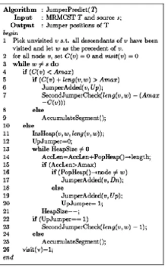
In this paper, we proposed a bottom-up approach to predict the jumper positions by inserting a minimum number of jumpers. Given a net and a source, we first hang the net by using the source as root. Then we compute the position of the jumper by accumulating interconnect length from each terminal in bottom-up fashion. To compute it, we have two possible scenarios as shown in Fig. 6. Line 4 considers whether the cumulative length C(v) of descendants of the terminal v (e.g., in Fig. 5(a), where d(ei) denotes the
length between the node v and the root of the i-th subtree and m denotes the number of subtrees) is less than the allowable antenna area (Amax). For this case,
there are two possible scenarios. First, if the sum of
C(v) and the length between v and its precedent w (i.e.
u(e)) does not exceed the Amax, we accumulate the total
length and the number of gates to w for further computation. Second, if the sum of C(v) and the length between v and its precedent w exceeds the Amax, we add
a jumper at the position near v (see Fig. 5(b)). After that, if the remaining length connecting to w also exceeds the Amax, we add a jumper at the position near
w. Line 10 considers whether the cumulative length of
descendants (C(v)) of the terminal v is greater than the allowable antenna area (Amax). For this case, we first
rank the length of edge adjacent to v in increasing order. If the cumulative length exceeds the Amax, we add a
jumper at the edge near v (see Fig. 5(c)). If we add a jumper at the edge (v, w), then goto Line 4. The algorithm is summarized in Fig. 6.
Given a net with n nodes, the best case time complexity of our jumper-prediction algorithm is O(n) when the cumulative length of descendants for all nodes is less than the allowable antenna area (Step 4 ~ 9). And the worst case time complexity happens when the net topology is a star graph (all the nodes are connected to the source directly) and the cumulative length of descendants for a source is greater than the allowable antenna area(Step10 ~ 26).
Since thecomplexity is
Fig. 5 (a) The initial case before the jumper-prediction process (b) The case of 1 ( ) max
m i i=d e <A
∑
, but 1 ( ) ( ) max m i i=d e +u e >A∑
, we add a jumper on u(e) then doSecondJumperCheck (c) The case of 1 ( ) max
m i i=d e >A
∑
, we accumulate the length of edges adjacent to v in increasing order. If the cumulative length exceeds the Amax, we add a jumper at the edge near vT1 T2 Tm d(e1) d(e 2) d(em) u(e) w v Jumper T1 T2 Tm
d(e1) d(e2) d(em)
u(e)
w
v
T1 T2 Tm
d(e1) d(e2) d(em)
u(e)
w
v
Fig. 6 Algorithm for Jumper Prediction
determined by sorting, the worst case time complexity is
O(n lg n).
By this algorithm, we can predict which edges are needed to insert jumpers. After that, we first break in two those segments of two-pin nets that need jumpers for reducing the amount of charging, if the length of those segments exceeds the minimum allowable gate- strength. If they have not exceeded the minimum allowable gate-strength, then we try to assign the remaining segments to the highest layer for “long jumpers.” If the highest layer is too congested, we assign segments to the lower layer and fix them by adding jumpers near the gate input using distance-aware maze routing after the track assignment phase.
3.3 Multilevel Routing with Antenna
Avoidance
After the jumper positions are predicted, our multilevel framework starts by coarsening the finest tiles of level 0. At each level, tiles are processed one by one, and only local nets (connections) are routed. At each level, a fast congestion-driven pattern routing [7]
is used for global routing.
After the global routing is completed, in order to break the cumulative length from the gates, we first break in two those segments of two-pin nets that need jumpers, if the length of those segments exceeds the minimum allowable gate-strength. If they have not exceeded the minimum allowable gate-strength, then we try to assign the remaining segments to the highest layer. If the highest layer is too congested, we assign segments to the lower layer and fix them by adding jumpers near the gate input using distance-aware maze routing after the track assignment phase. Then, an intermediate step of track assignment between coarsening and uncoarsening stages is used for fast routing completion and antenna avoidance.
The track assigner works on a full row or column of the global cell array at a time. To simplify the track assignment problem, we only assign segments which span more than one complete global cell in a row or a column, and handle short segments during detailed routing.
Let T be the set of tracks inside a panel. Let l be the set of segments which need to be track assigned in this panel. Each track t∈T can be represented by its set of constituent contiguous intervals. Denoting these intervals by xi, we have t ≈ ∪xi, Each of this xi is either
(1) a blocked interval, where no segment from l can be assigned, (2) an occupied interval, where no segment from l has been assigned, or (3) a free interval, where no segment from the set l has yet been assigned.
A segment seg∈l is called a left (right) segment, if the left- (right-)end terminal is in the left (right) zone. If a segment is said to be assignable to t∈T, t ≈ ∪xi, iff
xi∩ seg ≠ φ, it implies that either xi is a free interval or
it is an interval occupied by a segment of the same net. Thus, an antenna-aware track assignment problem can be defined as:
Antenna-Aware Track Assignment Problem: Given a set of tracks T in a panel and a set of segments l, and a cost function F : l × T → N, which represents the cost of assigning a segment to a track, find an assignment that minimizes the sum of the costs of the assignment.
In our implementation, we have considered the basic cost metrics such as the planar anchoring cost and the track and via obstruction cost. To better utilize the tracks in the panel, we will try to assign the left and right segments to the tracks in the bottom-up fashion. After these segments have been assigned, other segments are assigned by the well-known left-edge algorithm for efficient track assignability. Furthermore, these segments for track assignment are long and may violate the antenna rules. If the segments need jumpers after the jumper-prediction phase, we just add jumpers
at the two end sides, floating the segments so that they won’t cause damage to gates. Thus, track assignment is a suitable stage to address antenna avoidance.
After the track assignment phase, the actual track position of a segment is known. Thus, we can perform maze routing to complete the routing. After that, we perform an antenna check for every terminal. Since the accumulated gate-strength is kept in every terminal, the antenna-check process can be performed quickly. An accurate damage function which considers all plasma-based manufacturing operations is adopted for the antenna check. If nets have antenna violations, we regard them as failed nets to be routed at the uncoarsening stage. The uncoarsening stage starts to refine each local failed net (connection), remaining from the coarsening stage that has not passed the antenna check. The global router is now changed to the maze router. Also, a distance aware detailed maze routing is performed after the global maze routing. Uncoarsening continues until the first level G0 is
reached and the final solution is found.
4. EXPERIMENTAL RESULTS
We have implementedour multilevel system with
antenna avoidance in the C++ language on a 1 GHz SUN Blade 2000 workstation with 1 GB memory. See Table 1 for the benchmark circuits. The design rules for wire/via widths and wire/via separation for detailed routing are the same as those used in [7].
Table 1 describes the set of benchmark circuits. In the table, “Size” gives the layout dimensions, “#Layers” denotes the number of routing layers used, “#Nets” represents the number of two-pin connections after net decomposition, “#Diffusions” represents the number of diffusions (drivers), and “#Gates” represents the number of receiver type terminals.
Experimental results on wirelength, vias, run-time, violated gates, and delay are listed in Table 2, where “Davg” represents the average net delay. To perform
experiments on timing-driven routing, we used the same resistance and capacitance parameters as those used in [7] for comparison. A via is modeled as the π-model circuit, with its resistance and capacitance being twice those of a wire segment. And as mentioned in [12], we set Amax to 100 micron meter in this experiment.
Compared with [7], the experimental results show that our router reduced 100% antenna-violated gates and resulted in fewer increases in wirelength, vias, run-time, and delay.
Table 1 The benchmark circuits
Circuits Size (μm) #Layer #Nets #Diffusions #Gates
S5378 4330 × 2370 3 3124 1694 3040 S9234 4020 × 2230 3 2774 1486 2699 S13207 6590 × 3640 3 6995 3781 6781 S15850 7040 × 3880 3 8321 4472 8094 S38417 11430 × 6180 3 21035 11309 20901 S38584 12940 × 6710 3 28177 14753 27836
Table 2 Results of wirelength, vias, violated gates, run-time, and delay comparison
Results without antenna avoidance Our Results
Wirelength #Vias #Violated Gate Time Davg Wirelength #Vias #Violated Gate Time Davg
S5378 8.4e7 7451 129 10.6 1258 8.4e7 7533 0 12.5 1271 S9234 6.0e7 6239 75 8.1 1009 6.1e7 6315 0 10.9 1015 S13207 2.3e8 16003 304 22.6 1243 2.4e8 16242 0 29.9 1281 S15850 2.9e8 19126 354 62.6 1253 3.0e8 19534 0 75.8 1279 S38417 8.0e8 49816 683 71.3 1146 8.2e8 50521 0 86.9 1171 S38584 1.1e9 65798 974 255.6 1151 1.2e9 67068 0 307.0 1194
5. CONCLUSION
In this paper, we have proposed a novel framework for multilevel full-chip routing with antenna avoidance using a built-in jumper insertion approach. The experimental results have shown that our algorithm is very efficient and effective. Our future work lies in multilevel routing considering other nanometer electrical effects.
REFERENCES
[1] P. H. Chen, S. Malkani, C.-M. Peng and J. Lin, “Fixing antenna problem by dynamic diode dropping and jumper insertion,” Proc.
International Symposium on Quality Electronic Design, 2000, pp. 275−282.
[2] Z. Chen and I. Koren, “Layer reassignment for antenna effect minimization in 3-layer channel routing,” Proc. Workshop on DFT, 1996, pp. 77−85.
[3] J. Cong, J. Fang and Y. Zhang, “Multilevel approach to full-chip gridless routing,” Proc.
International Conference on CAD, Nov. 2001, pp.
396−403.
[4] J. Cong, M. Xie and Y. Zhang, “An enhanced multilevel routing system,” Proc. International
Conference on CAD, Nov. 2002, pp. 51−58.
[5] J. Cong and J. Shinnerl, Multilevel Optimization in
VLSICAD, Kluwer Academic Publishers, 2003.
[6] H. T. Heineken, J. Khare, W. Maly, P. K. Nag, C. Ouyang and W. A. Pleskacz, “CAD at the design-manufacturing interface,” Proc. Design
Automation Conference, June 1997, pp. 321−326.
[7] T.-Y. Ho, Y.-W. Chang, S.-J. Chen and D. T. Lee, “A fast crosstalk- and performance-driven multilevel routing system,” Proc. International
Conference on CAD, Nov. 2003, pp. 382−387.
[8] L.-D. Huang, X. Tang, H. Xiang, D. F. Wong and I.-M. Liu, “A polynomial time optimal diode insertion/routing algorithm for fixing antenna problem,” Proc. Design, Automation and Test in
Europe, 2002, pp. 470−475.
[9] A. B. Kahng, “Research directions for coevolution of rules and routers,” Proc. International
Symposium on Physical Design, Apr. 2003, pp.
122−125.
[10] R. Kastner, E. Bozorgzadeh and M. Sarrafzadeh,
“Pattern routing: use and theory for increasing predictability and avoiding coupling,” IEEE Trans.
on CAD, Nov. 2002, pp. 777−790.
[11] S. Krishnan, S. Rangan, S. Hattangady, G. Xing, K. Brennan, M. Rodder and S. Ashok, “Assessment of charge-induced damage to ultra-thin gate MOSFETs,” Proc. International Electron Devices
Meeting, 1997, pp. 445−448.
[12] H. K.-S. Leung, “Advanced routing in changing technology landscape,” Proc. International
Symposium on Physical Design, Apr. 2003, pp.
118−121.
[13] S.-P. Lin and Y.-W. Chang, “A novel framework for multilevel routing considering routability and performance,” Proc. International Conference on
CAD, Nov. 2002, pp. 44−50.
[14] W. Maly, C. Ouyang, S. Ghosh and S. Maturi, “Detection of an antenna effect in VLSI designs,”
Proc. International Symposium on Defect and Fault Tolerance in VLSI Systems, Nov. 1996, pp.
86−94.
[15] R. H. J. M. Otten, R. Camposano and P. R. Groeneveld, “Design automation for deepsubmicron: present and future,” Proc. Design,
Automation and Test in Europe, 2002, pp.
650−657.
[16] L. K. Scheffer, “Physical CAD changes to incorporate design for lithography and manufacturability,” Proc. Asia Pacific Design
Automation Conference, 2004.
[17] H. Shin, C.-C. King and C. Hu, “Thin oxide damage by plasma etching and ashing process,”
Proc. International Reliability Physics Symposium,
1992, pp. 37−41.
[18] H. Shirota, T. Sadakane, M. Terai and K. Okazaki, “A new router for reducing ‘Antenna effect’ in ASIC design,” Proc. Custom Integrated Circuit
Conference, Sept. 1998, pp. 27.5.1−27.5.4.
[19] K. P. Wang, M. Marek-Sadowska and W. Maly, “Layout design for yield and reliability,” Proc.
Physical Design Workshop, Apr. 1996, pp.
190−197.
[20] H. Watanabe, J. Komori, K. Higashitani, M. Sekine and H. Koyama, “A wafer level monitoring method for plasma-charging damage using antenna PMOSFET test structure,” IEEE Trans. on
Semiconductor Manufacturing, May 1997, pp. 228−
Tsung-Yi Ho (
何 宗 易
) received the M.S. degrees in computer and information sciencefrom the National Chiao Tung University, Hsinchu, Taiwan, in 2001. He is currently working toward the Ph.D. degree in the Graduate Institute of Electrical Engineering, National Taiwan University, Taipei. During 2003 to 2004, he was a visiting scholar in the Department of Electrical Computer Engineering, University of California, Santa Barbara. During the spring of 2005, he was a visiting scholar in the Institute of Information, Production, and System, Waseda University, Kitakyushu, Japan. His current research interests include computer-aided design and multilevel routing for nanometer technology.
Yao-Wen Chang (
張 耀 文
) received the B.S. degree from National Taiwan University in 1988, and the M.S. and the Ph.D. degrees from the University of Texas at Austin in 1993 and 1996, respectively, all in computer science.Currently, he is a Professor in the Department of Electrical Engineering & the Graduate Institute of Electronics Engineering, National Taiwan University, Taiwan. He was with the VLSI design group of IBM T. J. Watson Research Center, Yorktown Heights, New York, in the summer of 1994. From 1996 to 2001, he was on the faculty of the Department of Computer and Information Science, National Chiao Tung University, Taiwan. His research interests lie in physical design automation, architectures, and systems for VLSI and combinatorial optimization.
Dr. Chang received 2004 Wu Ta-You Memorial Award from the National Science Council of Taiwan for his outstanding research performance, Best Paper Award at the 1995 IEEE International Conference on Computer Design (ICCD-95) for his work on FPGA routing, six Best Paper nominations from the 2005 ACM/IEEE Design Automation Conference (DAC’05) for his work on X-architecture multilevel routing, the 2004 ACM/IEEE Asia and South Pacific Design Automation Conference (ASP-DAC-04) for his work on temporal floorplanning, 2003 ACM Transactions on Design Automation of Electronic Systems for his work on rectilinear block placement using B*-trees, the 2002 IEEE/ACM International Conference on Computer-Aided Design (ICCAD-02) for his work on multilevel routing, the 2001 IEEE International Conference on Computer Design (ICCD-01) for his work on temporal partitioning, and the 2000 ACM/IEEE Design Automation Conference (DAC-2K) for his work on the B*-tree floorplan representation, and two Excellent Teaching Awards from National Taiwan University (ranked #1 in the Department for undergraduate course teaching) in 2004 and National Chiao Tung University (ranked #1 in the Department) in 2000. He currently serves on the technical program committees of a few important international conferences on VLSI design automation and circuit design, including ICCAD, ASP-DAC (Topic Co-Chair), DATE, ICCD, and APCCAS. He is a member of the IEEE Circuits and Systems Society, ACM, and ACM/SIGDA.
Sao-Jie Chen (
陳 少 傑
) received the B.S. and M.S. degrees in electrical engineering from the National Taiwan University, Taipei, Taiwan, R.O.C., in 1977 and 1982 respectively, and the Ph.D. degree in electrical engineering from the Southern Methodist University, Dallas, U.S.A., in 1988.Since 1982, he has been a member of the faculty in the Department of Electrical Engineering, National Taiwan University, where he is currently a full professor. During the fall of 1999, he was a visiting professor in the Department of Computer Science and Engineering, University of California, San Diego, U.S.A. During the fall of 2003, he held an academic visitor position in the Department of System Level Design, IBM Thomas J. Watson Research Center, Yorktown
Heights, New York, U.S.A. During the fall of 2004, he was a visiting professor in the Department of Electrical and Computer Engineering, University of Wisconsin, Madison, U.S.A. His current research interests include: VLSI physical design, Wireless LAN and Bluetooth IC design, and SOC hardware/software co-design.
Dr. Chen is a member of the Chinese Institute of Engineers, the Chinese Institute of Electrical Engineering, the Association for Computing Machinery, a senior member of the IEEE Circuits and Systems and the IEEE Computer Societies.
收稿日期93 年 11 月 30 日、接受日期 94 年 1 月 30 日 Manuscript received November 30, 2004, accepted January 30, 2005