行政院國家科學委員會專題研究計畫 期中進度報告
兆級晶片系統前瞻技術研究--子計畫七:兆級晶片系統模
擬與正規驗證之整合技術(2/3)
期中進度報告(精簡版)
計 畫 類 別 : 整合型
計 畫 編 號 : NSC 95-2221-E-002-359-
執 行 期 間 : 95 年 08 月 01 日至 96 年 07 月 31 日
執 行 單 位 : 國立臺灣大學電子工程學研究所
計 畫 主 持 人 : 黃鐘揚
處 理 方 式 : 期中報告不提供公開查詢
中 華 民 國 96 年 06 月 03 日
※※※※※※※※※※※※※※※※※※※※※※※※※ ※
※
兆級晶片系統前瞻技術研究-子計畫七
※
※
兆級晶片系統模擬與正規驗證之整合技術 (2/3)
※
※※※※※※※※※※※※※※※※※※※※※※※※※ ※
計畫類別:□個別型計畫 ▓整合型計畫
計畫編號:NSC 94-2215-E-002-035
執行期間:
95 年 8 月 1 日至 96 年 7 月 31 日
計畫主持人:黃鐘揚 台灣大學電機系暨電子所助理教授
共同主持人:
計畫參與人員:
葉護熺 台灣大學電子工程學研究所
黃紹倫 台灣大學電機工程學研究所
張啟文 台灣大學電子工程學研究所
林庭豪 台灣大學電子工程學研究所
李智群 台灣大學電子工程學研究所
吳濟安 台灣大學電子工程學研究所
執行單位:台灣大學電子工程學研究所
中 華 民 國
95 年 7 月 15 日
兆級晶片系統前瞻技術研究-子計畫七
兆級晶片系統模擬與正規驗證之整合技術 (2/3)
“Combining Simulation and Formal Verification Techniques for
Trillion-transistor-Scale System-on-Chip (TS-SoC) (2/3)”
計畫編號:NSC 94-2215-E-002-035
執行期間:95 年 8 月 1 日至 96 年 7 月 31 日
主持人:黃鐘揚 台灣大學電機系暨電子所助理教授
一、
中文摘要 本子計劃今年持續去年的進度,繼續在正規驗證引 擎以及RTL 設計除錯之輔助工具上進行研究,主要完 成的項目有二:(一) 針對複雜的電路結構所設計強健 的限制條件滿足產生器,以及 (二) 高階設計內涵自動 萃取演算法以提高設計驗證與除錯的效能。其中項目一 我們的限制條件滿足產生器之基本效能與現今世上最 快的產生器並駕齊驅,但是我們再加上針對複雜電路所 設計之專門演算法,我們的產生器之效能能夠在快上 15 到 20 倍。至於項目二我們開發出一套不限制於程式 碼風格之高階設計內涵自動萃取演算法,能夠自動的從 RTL 電路描述檔中萃取出各式各樣複雜的有線狀態自 動機以及計數器,這是連現今業界最先進的電子電路設 計自動化工具都做不到的事,這些演算法將有助於本計 劃在第三年實現智慧型的電路驗證與除錯工具。 關鍵詞:正規驗證,設計除錯,限制條件滿足產生器, 高階設計內涵,RTL 電路描述。 英文摘要In this year we continue to work on the formal verification engine and intelligent debugging algorithms. Specifically, we accomplished two major milestones: (1) we have implemented a robust circuit-based Boolean Satisfiability (SAT) engine for complex netlist structure, and (2) we devised an algorithm to automatically extract high-level design intents for intelligent RTL verification.
We have compared the performance of our circuit-based SAT solver with many state-of-the-art solvers. Our experimental results showed that with the baseline algorithm, our solver can achieve competitive performance. However, after we further add on more circuit structure-oriented algorithms, our solver can outperform the others by 15-20 times.
On the other hand, our high-level design intent extraction algorithm can automatically identify various types of constructs from the RTL hardware description files. We can extract explicit and implicit Finite State Machines (FSM) as well as the counters, which will be very useful for the future intelligent design verification and debugging. This feature is much more advanced even to the most prestigious industrial Electronic Design Automation (EDA) tools.
Keywords : formal verification, design debugging,
Boolean constraint satisfiability solver, high-level design intent, RTL hardware description files.
二、
限制條件滿足產生器In the past year, we have implemented a robust circuit-based SAT solver, called QuteSAT, in which its baseline solver (i.e. without using circuit information) can perform as well as the state-of-the-art Conjunctive Normal Form (CNF) solvers (e.g. zChaff [1] and miniSat [2]), and with just a little help from the circuit information, it can
our solver include: (1) a generic watching scheme that can seamlessly work on all kinds of circuit gates (simple or complex gates), (2) an implicit implication graph that enables efficient conflict-driven learning and (3) careful engineering work to implement most of the advanced SAT algorithm on the circuit data structure. For comparison purpose, we also implement a simple “J-frontier” algorithm to demonstrate that the circuit information can greatly help in the SAT problem.
We will briefly describe how we utilize algorithms like the generic watch scheme and the implicit implication graph to speed up the circuit-based SAT solver. The experimental results will also be presented in the following subsections.
2.1 Efficient Boolean Constraint Propagation
Boolean Constraint Propagation (BCP) is the most time consuming process in the SAT algorithm. It derives the logic implications in the deduction procedure. In a modern SAT solver, BCP may perform millions of implications per second, which is about 80% of the total SAT time [3]. Therefore, an efficient BCP is a critical factor for a powerful SAT solver.
With the “2-literal-watching” scheme, the BCP step implemented in CNF SAT usually yields a higher efficiency. Circuit SAT, on the other hand, usually adopts the “table-lookup” method for logic implications. This method is more efficient for circuits with limited gate types and with small number of fanins. However, for complex circuit structure, the “table-lookup” method may not be as efficient.
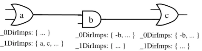
We propose several novel techniques to enhance the BCP process for the circuit SAT. First, we extract a direct implication graph during the circuit construction step as shown in Figure 1. It can greatly simplify the procedure of logic implications from single implication source.
For complex indirect implications, we devise a generic watching algorithm as shown below. It uses the concept of lazy evaluation and thus can significantly improve the BCP for primitive and complex circuit gates.
Generic watching algorithm for circuit SAT:
1. Let the output and input pins of the gate be the watched candidates. Let ‘n’ be the size of the watch candidate set.
2. Determine the ‘watched value” for each pin: if assigning a value ‘v’ on this pin may eventually lead to an indirect implication on other pin(s), then ‘v’ is the watched value of this pin. For example, assigning a ‘1’ to the input of an AND, or ‘0’ to a variable of a PB constraint may eventually lead to an indirect implication. Therefore, ‘1’ and ‘0’ are their watched values, respectively. On the other hand, for an XOR or MUX gate, both ‘0’ and ‘1’ may lead to indirect implications. Therefore, their watched value is “known”.
3. Find a minimum subset of watched candidates so that (a) assigning watched values on all the variables of the subset will produce an indirect implication, but (b) removing any of these assignments will void the implication. Let ‘k’ be the size of this subset.
4. We will need (n – k + 1) watched pointers.
5. Whenever there are assignments on the non-watched pins, or non-watched value assignments on the watched pins, we do nothing. The update of the watched pointer is called only when there is a watched-value assignment on the watched pin.
b
Fig 1. Direct implications graph
_0DirImps: { -b, ... } _1DirImps: { ... } _0DirImps: { -b, ... } _1DirImps: { ... } _0DirImps: { ... } _1DirImps: { a, c, ... }
2.2 Engineering an efficient circuit SAT
In order to implement an efficient circuit-based SAT solver, we adopt most of the advanced CNF SAT algorithms, and then further improve it by the circuit specific techniques. The outline of our SAT algorithm is similar to most of the CNF-based SAT (e.g. [1]). For example, Modern SAT solvers apply various learning techniques to prune out the search space [4][5]. In CNF SAT, learned information is stored as clauses such that the SAT algorithms can be applied on both the original and the new clauses. In circuit SAT, on the other hand, the learned information is usually recorded as attached AND gates with tied ‘0’ at the outputs. Therefore, the circuit SAT algorithms can then be executed on the same data structure.
Moreover, during the learning process, it is essential to figure out the causes of the implications. An intuitive way is to store this information as an explicit implication graph. However, this requires an extra amount of storage, and may lead to great overhead in the backtracking process. We propose an implicit implication recording method for circuit-base SAT as follows:
Implicit implication graph construction:
1. If the implication type is “DIRECT”, then the antecedent pointer is the single implication source. 2. If the implication type is “INDIRECT”, then the
implication sources are the watched candidates of the antecedent gate that are (a) non-watched variables, and (b) watched variables with watched values, excluding the implied pin.
2.3 Experimental Results
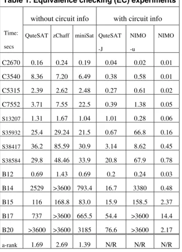
We conduct our experiments on the Equivalence Checking (EC) problems for the benchmark circuits. The benchmark we use include ISCAS 85/89 and ITC99 circuits. We use the logic synthesis tool ABC [6] to map the circuit into two different cell libraries, one including
complex gates, and the other with primitive gates only. The CNF representation is based on the Tseitin transformation. We select two state-of-the-art CNF SAT solvers: zChaff [1] and miniSat [2], and one well-known circuit-based SAT solver: NIMO [7], for comparison. All the experiments are conducted on a 3.2GHz Linux machine with 2GB memory.
We categorize our experiments into two sets: one without the use of circuit information — CNF SAT and our baseline solvers belong to this category. The other utilizes the circuit information in different ways — our “-J” option turns on the J-frontier technique, and the default NIMO applies signal correlation learning. As for the “-u” option of NIMO, it turns off the “explicit learning”. However, based on our observation1, it is still
somehow taking the advantage of the circuit information. The experimental results in Table 1 show that our baseline solver can achieve the comparable performance with the fastest CNF solvers. To the best of our knowledge, this is the first time that a circuit-based SAT solver can be as efficient as the CNF one while still retains the complete circuit information. This is mainly owing to our generic watching scheme for general gate types and the implicit implication graph that facilitates the fast conflict-driven learning.
On the other hand, the J-frontier method is a heuristic that should be effective not only for the EC problem but also for the general SAT problems like property checking. It concentrates on the most relevant search space, and with the advanced technique like “decision restart”, our experimental results show that our circuit SAT can constantly beat the CNF SAT solvers for 15+ times.
The other circuit-based SAT solver “NIMO” utilizes the signal correlation learning which is especially useful
1 We conducted EC on structurally identical circuits and found that
NIMO (even with –u) made 0 decision (of course no conflict) and finished in 0 time. This is impossible for all the other SAT solvers that do not use circuit (hashing) information.
pairs of signals (like most of the commercial EC tools do), it is no surprise that their solver can achieve the best result.
Table 1. Equivalence checking (EC) experiments
without circuit info with circuit info
Time: secs
QuteSAT zChaff miniSat QuteSAT -J NIMO -u NIMO C2670 0.16 0.24 0.19 0.04 0.02 0.01 C3540 8.36 7.20 6.49 0.38 0.58 0.01 C5315 2.39 2.62 2.48 0.27 0.61 0.02 C7552 3.71 7.55 22.5 0.39 1.38 0.05 S13207 1.31 1.67 1.04 1.01 0.28 0.06 S35932 25.4 29.24 21.5 0.67 66.8 0.16 S38417 36.2 85.59 30.9 3.14 8.62 0.45 S38584 29.8 48.46 33.9 20.8 67.9 0.78 B12 0.69 1.43 0.69 0.2 0.24 0.03 B14 2529 >3600 793.4 16.7 3380 0.48 B15 116 168.8 83.0 15.9 158.5 2.37 B17 737 >3600 665.5 54.4 >3600 14.4 B20 >3600 >3600 3185 76.6 >3600 2.17 a-rank 1.69 2.69 1.39 N/R N/R N/R
三、
高階設計內涵自動萃取演算法We propose a novel high-level design intent extraction technique that can identify explicit, implicit FSMs and counters with varied coding styles. Our approach is backed up by several theorems that can ensure the robustness of our algorithm. We have tested our program on several public and private benchmarks and the results show that our tool can extract much more high-level design intents than the commercial ones. For the explicit FSMs that the commercial tools can extract, we also carefully compare them with our results in order to make sure the correctness of our program. With the successful high-level design intent extraction engine, we
in the future.
3.1 Explicit FSM Extraction
We define HDL-independent “explicit FSM (ex-FSM)” as follows:
Definition 1 (Explicit FSM):
An explicit FSM has the following properties:
(1) Its number of states, state encoding and reset state are explicitly defined.
(2) For each state, its next state function is explicitly defined in a separate statement.
An example of explicit FSM is as shown in Figure 2. Given a RTL netlist, we will first perform HDL analysis to extract the key controlling and possible state variables. After collecting these key signals from the design module, we will base on the following theorems to extract the explicit FSMs.
Theorem 1: State variable recognition of explicit FSM
If a signal v ∈ PSV is a state variable of an explicit FSM, then there exists a signal w ∈ SIGS, such that w ∈ v.ACS,
v ∈ w.ADS, and | w.ADS | = 1.
Example: As mentioned above, the PSV for “demo1” is
{ ns, go }. We can find a signal “cs” such that “cs ∈ ns.ACS”, “ns ∈ cs.ADS” and “| cs.ADS | = 1. On the other hand, there is no such signal for “go”. Therefore, “ns” is the only state variable for the ex-FSM.
As for the reset state of an ex-FSM, we have the following lemma:
Lemma 1.1: Reset state recognition of explicit FSM
Let v and w be the signals of an extracted ex-FSM as defined in Theorem 1, then there exists an assignment node l with constant source expression c (i.e. c = l.SE), such that v = l.TS, signal(l.AC) ∩ (v.ADS ∪ { w }) = ∅, and c is the reset value for the state variable v.
Example: In “demo1”, it can be shown that the only
assignment that satisfies lemma 1 is lines 9-10 “if (rst) ns <= 2’b00”. The other assignments will have non-empty intersection { ns }. Therefore, the reset signal is “rst” and the reset state is “2’b00”. □
STG generation of explicit FSM: Once the state
variable(s) and the reset state have been recognized, the STG of an ex-FSM can be easily derived from the assignment list of the state variable(s). For example, in line 16 of the design “demo1”, since we know that “cs” is the output of the state transition function (Theorem 1) and “reset” is the reset signal, the current state must be “2’b00”, and the state transition condition can be simplified as “en”. The next state, therefore, should be the source expression “2’b10”.
3.2 Implicit FSM Extraction
In practical HDL designs, however, it is not always possible to explicitly define the set of legal states, and it may be more code-efficient to describe the state transitions as functions of state variables, instead of enumerated constant (state values). Therefore, we define the term “implicit FSM (imp-FSM)” as follows:
Definition 2 (Implicit FSM):
An implicit FSM has the following properties:
(1) Its number of states, state encoding and reset state may not be explicitly defined.
(2) Some of its state transition functions are implicitly defined in terms of state variables (and maybe with other variables).
An example of implicit FSM is as shown in Figure 3. We use the following theorem to identify implicit FSM:
Similar to explicit FSMs, we follow the theorems below to extract the implicit FSMs.
Theorem 2: State variable recognition of implicit FSM
If a signal v ∈ PSV is a state variable of an implicit FSM, then there exists a signal w ∈ SIGS, such that ⎯
case 1. w ∈ v.ADS and v ∈ w.ADS, or case 2. w ∈ v.ACS, v ∈ w.ADS, and | w.ADS | > 1.
Example: The ADS and ACS of signals of “demo2” is as
shown in Table 3. Since d1 ∈ PSV, d1 ∈ d2.ADS, and d2 ∈ d1.ADS, this is an implicit FSM with d1 as the state variable. □
Reset state recognition of implicit FSM: Since the reset
state of the implicit FSM may not be explicitly defined, the method in Lemma 1.1 may not work. However, if such reset state is indeed explicitly specified, we can still recognize it through this lemma. For example, we can recognize the reset state of “demo2” as “d1 = 0”, and the reset signal as “~reset”.
STG generation of implicit FSM: We use Binary
Decision Diagram (BDD) to construct the STG of the imp-FSM. Without loss of generosity, let’s assume the assignments for the combinational and sequential logic are grouped in two different blocks, as shown in Figure 8, where X and Y are the outputs of the sequential and combinational blocks, respectively. Let Y = comb(X, ∑x),
and X = seq(Y, ∑y), where “comb” and “seq” are the state
Figure 2. An example of explicit FSM
1 … 2 reg [1:0] ns; 3 reg go; 4 wire [1:0] cs; 5 … 6 assign cs = ns; 7 … 8 always @ ( posedge clk or posedge rst ) begin 9 if ( rst ) begin 10 ns <= 2'b00; 11 go <= 1'b0; 12 end 13 else begin 14 go <= ( cs == 2'b10 ) & en; 15 case ( cs ) 16 2'b00: ns <= ( en ) ? 2'b10: 2'b00; 17 2'b10: ns <= ( en ) ? 2'b01: 2'b10; 18 2'b01: ns <= ( en ) ? 2'b00: 2'b01; 19 default: ns <= 2'b00; 20 endcase 21 end
22 end
23 …
cones. We first build BDD for the transition relationship from X to Y, that is, BDD(Y, X, ∑x). Then we build the
BDD for the transition relationship from Y to X. However, in order to distinguish the later X (next cycle) from the previous one, we denote it as X+ and thus the BDD as
BDD(X+, Y, ∑
y). The next step is to use BDD “compose”
operator to compose these two BDDs and remove the variable Y away. Finally, we get the BDD(X+, X, ∑
y, ∑x)
and the STG can be obtained by traversing the cubes on this final BDD.
3.3 Counter Extraction
The state variable reorganization of a counter can be the same as described for the explicit or implicit FSMs. However, if we find that any of the assignments on the state variables contains arithmetic operators (e.g. “+”, “-”), we will calssify it as a counter. As mentioned above, the number of states in a counter can be very huge. Therefore, we do not explicitly enumerate the states nor generate the STG. Instead, we extract its characteristic function in a tabular format and create a high-level netlist that can help visualize the counter behavior.
high-level netlist of a counter can be represented as, from left to right, “assignments Æ multiplexer Æ counter registers” pattern. The “counter registers” are recognized as the state variables, while the controlling variables of the multiplexer correspond to the signals in the “active conditions (AC)” of the states. On the other hand, the inputs of the multiplexer (i.e. the constant or conditional assignments) are the “target expressions (TE)” and perhaps plus the “active conditions (AC)”of the state variables.
3.4 Experimental Results
We have implemented the proposed algorithm in C++ on top of our homegrown Verilog HDL parser (to be published later). The experiments were conducted on several RTL designs from OpenCores[8], other design
Figure 3. An example of implicit FSM
Figure 4. An example of counter (AES)
...
assign ns[0] = cs[1] | cs[2]; assign ns[1] = cs[0] & insert; assign ns[2] = cs[1] & select;
always @ ( posedge clk or posedge rst ) begin if (rst) cs = 1; else cs = ns; end ... ... always @ (posedge CLK) begin if(!RST_n) begin if (En_De) Nr<=4'd1; else Nr<=4'd10; end else begin if ((En_De&& Nr==4'd10)|| (!En_De && Nr==4'd1)) Nr<=Nr; else begin if (En_De)Nr<=Nr+4'd1; else Nr<=Nr-4'd1; end end end end ... ================================================== Counter: Nr[Width=4, MSB=3, LSB=0]
RST_n En_De Nr Action Description
0 0 x Nr = 10 Reset 0 1 x Nr = 1 Reset 1 0 == 1 Nr = Nr Bound condition 1 1 == 10 Nr = Nr Bound condition 1 0 !=1 Nr = Nr – 1 Down count 1 1 !=10 Nr = Nr + 1 Up Count En_De Nr==10?Nr=10: Nr++ Nr==1 ? Nr=1 : Nr-- 10 1 Reg ister Nr RST_n 0 0 1 2 3
team in our institute[9], and Sun Microsystems (“picoJava”)[10].
We compare our extracted results with two commercial tools ⎯ Debussy[11] and Design Compiler[12]. As shown in Table 2, our tool is the only one that supports all ex-FSM, imp-FSM, and counter extractions. Debussy (DB) supports ex-FSM extraction, but not the others. We have compared their extracted ex-FSMs with ours and it shows that both are exactly matched. On the other hand, Design Compiler (DC) supports only partial ex-FSM extraction. Without the help of compiler directives, it can only identify ex-FSMs with explicit “case-statement” style. If there is any other assignment mixed in the same block (e.g. FSM output logic), DC will not be able to recognize it.
Table 3 shows our FSM and counter extraction results. Please note that they are from real RTL designs and most of them are very complicated. Taking the “USB” design as an example [8], it is from the DMA unit and the source code contains 553 lines, 1 module, and 33 “always” blocks. Our extraction algorithm can successfully identify the FSM and use its symbolic name as the FSM states. This is very useful for design verification and debugging as we will discuss in the next section.
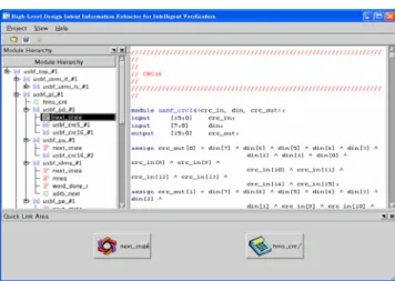
3.5 Graphical User Interface (GUI)s
We also provide a comprehensive Graphic User Interface( GUI ). Figure 5 shows the layout of our GUI window. There are three sub-windows as follows:
¾ Module Hierarchy Window:
This shows the design hierarchy. The extracted information is also listed in this window. Double click on the item (module, FSM, or counter) of your interest, the program will open the corresponding information automatically.
¾ Code Viewer Window:
This is a source code editor that supports syntax highlight. User can compare extracted control units (CUs) and their corresponding source code information.
¾ Quick Link Window:
This provides an area to store quick link of extracted CUs. For large designs, user may need to view several CUs at the same time. Instead of opening all of them on the desktop or closing them frequently, user can place temporarily inactive CUs in this window, and when they are needed later, just clicks the quick link button, and the program will open its corresponding information.
Figure 14 shows the layout of the Detail Viewer
window. There are two views: FSM view and counter
view. Once user double clicks the control unit listed in the Module Hierarchy window, the Detail Viewer is opened automatically and displays detail information. If user hides the Detail Viewer, the program will add one quick link button to the Quick Link window so that user can easily go back. For FSMs, Detail Viewer shows the State Transition Graph/Table and the analysis result including
Table 2: Comparison of results DB DC Ours ex-FSM ○ △ ○ imp-FS M ╳ ╳ ○ Counter ╳ ╳ ○
Note:○ Fully supported △ Partially ╳ Not Supported
Table 3: Summary of result
ex-FSM imp-FSM counter
AC97 0 0 9 USB 6 0 16 AES 1 0 1 Router 1 0 1 OCRS 2 0 3 RCRS 3 0 4 Contest 2 2 0 PicoJava 3 18 1
counter, the Detail Viewer shows the operation table (see Fig.14(b)). As shown in figure 14(a), we can easily see that the reset state is 3’ 001, dead state is 3’b000, and there are two unreachable states: 3’b100 and 3’b110.
四、 未來一年的計畫與目標
In the coming year (i.e. the last year of this 3-year project), we will integrate the techniques developed in formal verification, RTL design analysis, and simulation. Our first target is to create an intelligent test pattern generator for large and complex RTL designs. In such designs, traditional methods like formal verification or simulation alone will not be able to achieve satisfactory functional coverage. We will automatically generate test sequence for the uncovered part of codes and thus help designer to verify the correctness of the designs.
We will also apply the above techniques to design debugging. With the automatic design intent extractor and powerful Boolean reasoning engine, we will be able to analyze the cause of the design bugs and provide suggestions to the designer for the error correction.
Our work will also contribute to the publications in the coming year. We will target on the major EDA conference such as Design Automation Conference (DAC, deadline in late November) and International Conference on Design Automation (ICCAD, deadline in mid-April). At the end, the work will be summarized and submitted to selected
五、 參考文獻
1. M.W. Moskewicz, C.F. Madigan, Y. Zhao, L. Zhang, and S. Malik, “Chaff: engineering an efficient SAT solver”, DAC 2001, pp. 530 – 535.
2. N. Een and N. Sörensson, “MiniSat: A SAT solver with conflict clause minimization”, SAT ’05.
3. M.K. Ganai, L. Zhang, P. Ashar, A. Gupta, and S. Malik, “Combining strengths of circuit-based and CNF-based algorithms for a high performance SAT-solver”, DAC 2002, pp. 747-750.
4. J.P. Marques-Silva and K.A. Sakallah, “GRASP-A search algorithm for propositional satisfiability”, T. Comp., vol. 48, pp. 506 – 521, 1999.
5. S. Shuo and M. Hsiao, “Success-driven learning in ATPG for preimage computation”, Design & Test of Computers 2004, pp. 504- 512.
6. http://www.eecs.berkeley.edu/~alanmi/abc, “ABC: A system for sequential synthesis and verification” 7. http://cadlab.ece.ucsb.edu/downloads/nimo.html,
“Sequential Circuit SAT Solver Homepage”. 8. http://www.opencores.org, OpenCores.
9. Access Lab, Graduate Institute of Electronics Engineering, National Taiwan University.
10. http://www.sun.com/software/communitysource/proce ssors/download_picojava.xml, “picoJava-II v2.0 source code”, Sun Microsystems.
11. http://www.springsoft.com “Debussy Debug System”, SpringSoft, Inc.
12. http://www.synopsys.com, “Design Compiler”, Synopsys, Inc.
![Figure 4. An example of counter (AES) ... assign ns[0] = cs[1] | cs[2];](https://thumb-ap.123doks.com/thumbv2/9libinfo/8775608.213820/8.892.468.823.416.967/figure-an-example-of-counter-aes-assign-ns.webp)