後沉積之一氧化二氮氣體電漿處理對二氧化鉿堆疊式閘極金氧半場效電晶體電性之影響
100
0
0
全文
(2) 後沉積之一氧化二氮氣體電漿處理對二氧化鉿堆疊 式閘極金氧半場效電晶體電性之影響. Effects of Post-Deposition N2O Plasma Nitridation on the Electrical Characteristics of pMOSFETs with HfO2/SiON Gate Stacks 研 究 生:李聰杰 指導教授:黃調元. Student:Tsung-Chieh Lee 博士. Advisor:Dr. Tiao-Yuan Huang. 簡昭欣 博士. Dr. Chao-Hsin Chien. 國 立 交 通 大 學 電子工程學系 電子研究所碩士班 碩 士 論 文. A Thesis Submitted to Institute of Electronics College of Electrical Engineering and Computer Science National Chiao Tung University in Partial Fulfillment of the Requirements for the Degree of Master of Science in Electronic Engineering June 2005 Hsinchu, Taiwan, Republic of China. 中 華 民 國 九 十 四 年 六 月.
(3) 後沉積之一氧化二氮氣體電漿處理對二氧化鉿堆疊 式閘極金氧半場效電晶體電性之影響. 研究生 :. 李聰杰. 指導教授 : 黃調元 博士 簡昭欣 博士. 國立交通大學 電子工程系. 電子研究所碩士班. 摘要. 在元件尺寸快速微縮的需求下,傳統二氧化矽(SiO2)閘極介電層微縮到 2 奈米左右時, 其量子穿隧效應引致漏電流已大到無法忍受。為解決此問題,用高介電材質諸如二氧化 鉿(HfO2),以取代傳統二氧化矽,乃勢在必行。然而,高介電係數之閘極介電層仍有許 多待解問題,諸如,大量界面缺陷(interface state densities),大量本體缺陷(Bulk traps)等。 本論文中,我們嘗試使用一氧化二氮電漿氮化處理,以改善二氧化鉿閘極介電層的品質。 實驗中,我們發現一氧化二氮電漿氮化處理後,可以得到諸如較低閘極漏電流、較高 電導頂峰值(Gm peak value)、較佳次臨界擺幅(substhreshold swing)、較低界面缺陷、和較低 二氧化鉿本體缺陷等優點。在二氧化鉿閘極介電層中,電流傳導機制主要是 Frenkel-Poole;經過氮化處理後,電子缺陷的能階變深,靠近閘極之傳導帶。且經氮化. i.
(4) 處理後,原本呈現捕捉電洞之行為,會轉變成捕捉電子。我們也發現,在固定電壓應力 (CVS)、及負偏壓-溫度應力(NBTI)的可靠性測試中,電晶體之退化,乃緣於本體中之捕 捉行為,而非由界面缺陷的增加。在動態應力(dynamic stress)可靠性測試下,我們發現, 關閉時間(off-time)時釋放電洞之行為,及因開啟時間(on-time)太短,而來不及捕捉電洞, 二者均須加以考量,方能解釋動態應力下臨界電壓漂移之行為。透過載子分離(carrier separation)量測,我們得以釐清,崩潰究竟是發生於二氧化鉿本體或是界面層。. ii.
(5) Effects of Post-Deposition N2O Plasma Nitridation on the Electrical Characteristics of pMOSFETs with HfO2/SiON Gate Stacks. Student : Tsung-Chieh Lee. Advisor : Dr. Tiao-Yaun Huang Dr. Chao-Hsin Chien. Department of Electronics Engineering and Institute of Electronics National Chiao Tung University, Hsinchu, Taiwan. Abstract With aggressive device scaling, shrinking the conventional thin silicon dioxide gate dielectric to the range of 2nm has caused an unbearable direct tunneling leakage current. To solve the problem, it is necessary to replace SiO2 by some high-k dielectric materials such as HfO2. However, there are many outstanding issues in high-k materials, such as high interface state densities, large amounts of bulk traps, etc. In this thesis, we try to use post-deposition N2O plasma nitridation to improve the HfO2 film quality. We found that N2O plasma nitridation brings about many advantages such as reduced gate leakage current, increased Gm peak value, better subthreshold swing, reduced interface states and bulk traps in the HfO2. The dominant current transport mechanism in HfO2 gate dielectric iii.
(6) is of the Frenkel-Poole type, and the electron traps are located at a deeper energy position after N2O plasma nitridation. Also, the preponderant trapping behaviors become electron-trapping dominant, rather than hole-trapping dominant, after N2O plasma nitridation. Under the constant voltage stress (CVS) and negative bias temperature instability (NBTI), we found that bulk traps in HfO2, rather than interface state densities, are responsible for the transistor degradation. Under dynamic stress, both the off-time de-trapping and the lack of hole trapping due to short on-time are required to explain the behavior of threshold voltage degradation. Finally, through the help of carrier separation experiments, we have clarified whether the breakdown originates in the bulk or the interfacial layer.. iv.
(7) Acknowledgement 兩年的碩士班生活,即將告一個段落。兩年的碩士生涯中,得到許許多多人的幫助, 讓不長不短的兩年在充實與歡笑中度過,在此我必須要感謝所有陪我度過兩年交大生涯 的人。沒有你們就沒有這篇論文,沒有你們就不會有這 happy ending。 首先,在這裡一定要感謝的是三位良師也是益友, 黃調元博士, 簡昭欣博士,以 及 林鴻志博士,黃老師在實驗上周詳的思考方式,在專業以及非專業上的博覽,令學 生非常佩服,也在這態度上面學了許多,就像金字塔一般,要高聳入天就要有廣博努力 的第一層台階。簡博士在實驗過程中不厭其煩的教導解答,以及相信學生的態度讓我對 師生之間的關係有另一層的啟發。林老師在 meeting 中的諄諄教誨,以及要求以樂趣去 學習,去念懂 paper 更給學生一種不一樣層次的感受。在這裡要以最誠摯的心感謝你們 三位兩年來的教導。 其次,實驗室的學長也是要由衷的感謝,盧文泰泰學長在量測上的指導給了很大的 收穫,更別說在 paper 上的幫助了。呂嘉裕學長在實驗上的經驗,也讓我學習到很多, 讓我在 NDL 裡不會茫茫然。林宏年學長從京都帶回來的抹茶巧克力很好吃,還有葉冠 麟學長,李耀仁學長,李明賢學長,盧景森學長,蘇俊榮學長,陳永裕學長,陳世璋學 長,楊紹明學長,林育賢學長平日的照顧,兩年的相處一直都很快樂,謝謝你們。 此外,也要感謝 NDL 的工程師,員工,工作人員的協助幫忙,讓我順利完成元件 的製作,謝謝你們 還有同為碩二的新原,伊鋒,文廷,賢達,彥廷,祐慈,雁雅,昶維,宗翰,你們 的同甘苦共患難是值得回憶的。 也要感謝實驗室的八個碩一學弟帶給實驗室的生氣,徐行徽,洪振家,張凱祥,黃 健銘,趙志誠,蔡銑泓,呂建松,謝雨霖,嗯嗯,你們吵的很好笑。 還有女朋友芳如,沒事就吵吵我,當然也會在一旁支持我。 最後要感謝我的父母,妹妹,朋友,默默的給予我支持鼓勵,讓我順利的完成學業. v.
(8) Contents. Abstract (in Chinese) ……………………………………………….…… i Abstract (in English) ……………………………………………….….… iii Acknowledgement (in Chinese) ……………………………………..….… v Contents …..………………………………………………………....… vi Figure Caption …………………………………………………..……… viii. Chapter 1. Introduction. 1.1. Background ………………………………………………… p.1. 1.2. Why High-k Gate Dielectric? …………………………..…….. p.2. 1.3. The Choice of High-k Materials ………………………………. p.3. 1.3.1. Physical Properties ……………………………………...…... p.3. 1.3.2. Electrical Properties …………………………………………. p.4. 1.4. Organization of The Thesis ……………..……………………. p.5. Chapter 2. Improvements on the Electrical Characteristics of pMOSFETs with HfO2/SiON Gate Stacks by Post-Deposition N2O plasma Treatment. 2.1. Introduction ……………………………………………….... p.6. 2.2. Experimental Procedure …………………………………….... p.7. 2.3. Results and Discussion …………………………....……..…... p.8. 2.3.1. Electrical Properties of HfO2/SiON Gate Dielectrics ………..…... p.8. 2.3.2. Charge Pumping Measurements …………………………...….. p.9 vi.
(9) 2.3.2.1. Fixed Amplitude Sweep …………………………………....... p.9. 2.3.2.2. Fixed Base Sweep and Fixed Peak Sweep …………..………..... p.11. 2.3.3. Constant Gate Overdrive Stress ……………………………..... p.13. 2.3.4. Current Transport Mechanism …………………..………..…... p.14. 2.4. Summaries ……………………………..……………….….. p.17. Chapter 3. Impacts on the Reliability of HfO2/SiON Gate Stacks by Post-Deposition N2O Plasma Treatment. 3.1. Introduction ……………………………………………..... p.18. 3.2. Results and Discussion ………………………...………....... p.18. 3.2.1. Appropriate Measurement Setup for High-k Gate Dielectrics ….. p.18. 3.2.2. Breakdown Investigation by Carrier Separation Method …...….. p.20. 3.2.3. Dynamic Stress ………………………………………..….. p.22. 3.2.4. NBTI in HfO2/SiON Gate Stacks ……………………..…….. p.24. 3.3. Summaries ……………………………………………….. p.26. Chapter 4 Conclusion 4.1. Conclusion ……………………………………………….. p.28. Reference ………………………………………….………………….. p.29. Figure-Chapter 1 ……………………………………………………….. p.33 Figure-Chapter 2 ……………………………………………………….. p.35 Figure-Chapter 3 ……………………………………………………….. p.55 Vita ……………………………………………………………….…... p.84 vii.
(10) Figure Caption Chapter 1. Fig. 1-1 With the marching of technology nodes, gate dielectric has to be shrunk and five silicon atoms thick of gate dielectric is predicted for 2012. [1] Fig. 1-2 Measured and simulated Ig-Vg characteristics under inversion condition for nMOSFETs. The dotted line indicates the 1A/cm2 limit for the leakage current. [2] Fig. 1-3 Several high-k gate dielectric materials with their bandgaps and dielectric constants. [3] Fig. 1-4 Several high-k gate dielectric materials with their band offsets. [4]. Chapter 2. Fig. 2-1. Process flow.. Fig. 2-2. Gate leakage current of P+ poly-gated pMOSFETs with HfO2/SiON high-k gate stacks with (dashed line) and without (solid line) N2O plasma treatment both under inversion and accumulation regions.. Fig. 2-3. Capacitance-voltage characteristics measured at 100 kHz for the HfO2/SiON high-k gate stacks with and without N2O plasma treatment. The capacitance equivalent oxide thickness (CET) is determined by measuring the maximum inversion capacitance.. Fig. 2-4. Id-Vd characteristics of pMOSFETs with HfO2/SiON high-k gate stacks with and without N2O plasma treatment.. Fig. 2-5. Id-Vg characteristics of pMOSFETs with HfO2/SiON high-k gate stacks with and without N2O plasma treatment.. viii.
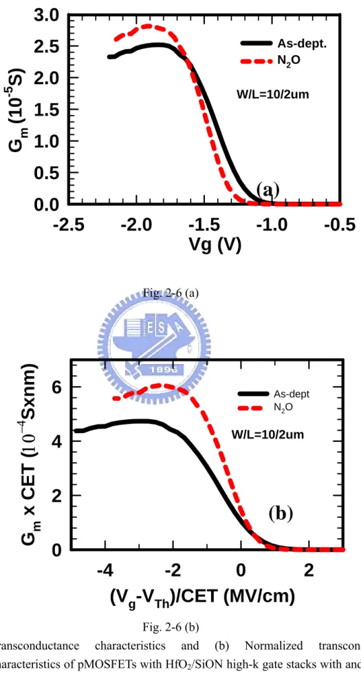
(11) Fig. 2-6. (a) Transconductance characteristics and (b) Normalized transconductance characteristics of pMOSFETs with HfO2/SiON high-k gate stacks with and without N2O plasma treatment.. Fig. 2-7. Setup structure for charge pumping.. Fig. 2-8. Schematic illustrations for the charge pumping measurement with (a) fixed amplitude, (b) fixed base sweep, and (c) fixed peak sweep. The arrows indicated the sweep direction.. Fig. 2-9. Charge pumping measurement results of Ncp and Nsd with (a) fixed amplitude sweep, (b) fixed base sweep, and (c) fixed peak sweep as a function gate pulse frequency for pMOSFETs with HfO2/SiON high-k gate stacks without N2O plasma treatment.. Fig. 2-10 Charge pumping measurement result of Icp and Isd with (a) fixed base sweep, and (b) fixed peak sweep as a function of gate pulse frequency for pMOSFETs with HfO2/SiON high-k gate stacks without N2O plasma treatment. The insets of both (a) and (b) are linear scale y axis. (i.e., insets in each figure is the linear scale) Fig. 2-11 Possible current components in charge pumping measurement for high-k gate dielectrics. (1) recombination current due to interface states. (2) recombination current of charging and discharging of bulk traps. (3) recombination current of inversion carriers due to geometric effect. (4) gate leakage current contribution. (5) minority carrier diffusion (not shown). [46] Fig. 2-12 Interface states density as a function of Vgl for HfO2/SiON high-k gate stacks with and without N2O plasma treatment measured by fixed amplitude sweep at frequency of 1 MHz. Fig. 2-13 Ncp and Nsd as determined from Icp and Isd by fixed base sweep at 5 kHz. Lower ix.
(12) bulk traps were obtained by applying N2O plasma treatment. Fig. 2-14 Dependence of threshold voltage shift (△Vthc) on injected charge densities (Ninj) under constant gate overdrive voltage of Vg-Vthc= -2.2V (open symbol) and Vg-Vthc= -2.6V (solid symbol). Fig. 2-15 Dependence of generated interface state densities (△Nit) and trapping charges (△ Ntot) on injected charge densities (Ninj) under constant gate overdrive stress voltage of Vgo=Vg-Vthc= -2.2V (open sympol) and Vgo=Vg-Vthc= -2.6V (solid sympol). Fig. 2-16 Carrier separation of as-dept. HfO2/SiON gate stacks under both inversion and accumulation regions. Fig. 2-17 Carrier separation of post-N2O-treated HfO2/SiON gate stacks under both inversion and accumulation region. Fig. 2-18 Band diagrams of HfO2/SiON gate stacks under inversion and accumulation. Under accumulation, the high-k mainly acts as a capacitive voltage divider and electrons enter the HfO2 conduction band. Fig. 2-19 Carrier separation results versus gate voltage for fresh as-dept. devices at various temperatures. Fig. 2-20 Carrier separation results versus gate voltage for fresh post-N2O-treated devices at various temperatures. Fig. 2-21 Frenkel-Poole plot for the source/drain current in the inversion region. Good fitting curves can be observed (solid lines) for the as-dept. sample. Fig. 2-22 Frenkel-Poole plot for the substrate current in the inversion region. Good fitting curves can be observed (solid lines) for the as-dept. sample. Fig. 2-23 Frenkel-Poole plot for the source/drain current in the inversion region. Good fitting curves can be observed (solid lines) for the post-N2O-treated sample. Fig. 2-24 Frenkel-Poole plot for the substrate current in the inversion region. Good fitting curves can be observed (solid lines) for the post-N2O-treated sample. x.
(13) Fig. 2-25 Energy band diagram for HfO2/SiON gate stacks, illustrating the conduction mechanism of Frenkel-Poole emission. Fig. 2-26 Energy band diagram for HfO2/SiON gate stacks, illustrating the conduction mechanism of Frenkel-Poole emission. Fig. 2-27 HRTEM images for (a) as-dept. sample and (b) post-N2O-treated sample.. Chapter 3. Fig. 3-1. Repetitive Id-Vg traces for HfO2/SiON high-k gate dielectric using measurement sequence (a) [Vg=0V ↔ Vg=-2V], (b) [Vg=1V ↔ Vg=-2V]. (w/o post-N2O plasma treatment).. Fig. 3-2. Repetitive Id-Vg traces for HfO2/SiON high-k gate dielectric using measurement sequence of [1V, -2V], [1V, -2.2V], … , to [1V, -2.8V] (w/o post-N2O plasma treatment).. Fig. 3-3. Repetitive Id-Vg traces for HfO2/SiON high-k gate dielectric using measurement sequence (a) [Vg=0V ↔ Vg=-2V], (b) [Vg=1V ↔ Vg=-2V]. (w/ post-N2O plasma treatment).. Fig. 3-4. Repetitive Id-Vg traces for HfO2/SiON high-k gate dielectric using measurement sequence of [1V, -2V], [1V, -2.2V], … , to [1V, -2.8V]. (w/ post-N2O plasma treatment).. Fig. 3-5. Dependence of carrier separation results of IG and IB on substrate bias of HfO2/SiON high-k gate dielectrics (w/o post-N2O plasma treatment).. Fig. 3-6. Dependence of carrier separation results of ISD on substrate bias of HfO2/SiON high-k gate dielectrics (w/o post-N2O plasma treatment).. Fig. 3-7. Dependence of carrier separation results of ISD, IG, and IB on substrate bias of HfO2/SiON high-k gate dielectrics (w/ post-N2O plasma treatment). xi.
(14) Fig. 3-8. Evolutions of three kinds of current, gate current (IG), S/D current (ISD), and the substrate current (IB) under negative constant voltage stress of -4.2V (w/o post-N2O plasma treatment).. Fig. 3-9. Current of (a) IG, (b) IB, (c) ISD versus gate voltage for Fresh, SILC, and SBD conditions (w/o post-N2O plasma treatment).. Fig. 3-10 Illustrations of damage situations under SILC (a), and after SBD (b) (w/o N2O treatment). Fig. 3-11 Evolutions of three kinds of current, gate current (IG), S/D current (ISD), and substrate current (IB) under negative constant voltage stress of -4.2V (w/ post-N2O plasma treatment). Fig. 3-12 Current of (a) IG, (b) IB, (c) ISD versus gate voltage for Fresh, SILC, and SBD conditions (w/ post-N2O plasma treatment). Fig. 3-13 Illustrations of damage situations under SILC (a) and after SBD (b) (w/ post-N2O plasma treatment). Fig. 3-14 Setup structure of AC stress with the definition of frequency, on-time, off-time, and duty cycle. Fig. 3-15 Dependence of generated interface state densities versus stress time for various stress voltage frequencies. Vgo=-2.2V for duty cycle of 50% (w/o post N2O plasma treatment). Fig. 3-16 Dependence of threshold voltage shift versus stress time for various stress voltage frequencies. Vgo=-2.2V for duty cycle of 50% (w/o post N2O plasma treatment). Fig. 3-17 Threshold voltage shift at stress time of 1000 seconds versus gate pulse frequency (w/o post N2O plasma treatment). Fig. 3-18 Dependence of △Nit and △Ntot on injected charge densities under dynamic stress and DC stress (w/o post N2O plasma treatment). Fig. 3-19 Dependence of generated interface state densities versus stress time for various xii.
(15) stress voltage duty. Vgo=-2.2V ( w/o post- N2O plasma treatment). Fig. 3-20 Dependence of threshold voltage shift versus stress time for various stress voltage duty cycles. Vgo=-2.2V at 10k Hz (w/o post- N2O plasma treatment). Fig. 3-21 Dependence of threshold voltage shift versus stress time for various stress voltage duty cycles. Vgo=-2.2V at 100 Hz (b), and 10 Hz (a). (w/o post- N2O plasma treatment). Fig. 3-22 Dependence of generated interface state densities versus stress time for various stress voltage frequencies. Vgo=-2.2V for duty cycle of 50% (w/ post N2O plasma treatment). Fig. 3-23 Dependence of threshold voltage shift versus stress time for various stress voltage frequencies. Vgo=-2.2V for duty cycle of 50% (w/ post N2O plasma treatment). Fig. 3-24 Dependence of threshold voltage shift versus stress time for various stress voltage duty cycles. Vgo=-2.2V at 1k Hz (w/ post-N2O plasma treatment). +. Fig. 3-25 Id,Gm-Vg characteristics for p gated pMOSFETs before and after 1000 seconds stress for (a) room temperature, and (b) 125℃ (w/o post-N2O plasma treatment). Fig. 3-26 Generated interface state densities as a function of stress time under BTI at various stress temperatures. Vgo=-1.5V (w/o post-N2O plasma treatment). Fig. 3-27 Threshold voltage shift as a function of stress time under BTI at various stress temperatures. Vgo=-1.5V (w/o post-N2O plasma treatment). Fig. 3-28 Dependence of △ Nit and △ Ntot on stress time under Vgo= -2V at various temperatures (w/o post-N2O plasma treatment). +. Fig. 3-29 Id, Gm-Vg characteristics for p gated pMOSFETs before and after 1000 seconds for (a) room temperature, and (b) 125℃ (w/o post-N2O plasma treatment). Fig. 3-30 Generated interface state densities as a function of stress time under BTI at various stress temperatures. Vgo=-2V (w/o post-N2O plasma treatment). Fig. 3-31 Threshold voltage shift as a function of stress time under BTI at various stress xiii.
(16) temperatures. Vgo=-2V (w/o post-N2O plasma treatment). Fig. 3-32 Dependence of △ Nit and △ Ntot on stress time under Vgo= -2V at various temperatures (w/o post-N2O plasma treatment). Fig. 3-33 Dependence of Id degradation on stress time under Vgo= -2V at various temperatures (w/o post-N2O plasma treatment). Fig. 3-34 Gate, source/drain, substrate currents for fresh pMOSFETs at various temperatures. Vgo=-2V (w/o post-N2O plasma treatment). +. Fig. 3-35 Id, Gm-Vg characteristics for p gated pMOSFETs before and after 1000 seconds for (a) room temperature, and (b) 125℃. (w/o post-N2O plasma treatment). Fig. 3-36 Threshold voltage shift as a function of stress time under BTI at various stress temperatures. Vgo=-2.5V (w/o post-N2O plasma treatment). Fig. 3-37 Dependence of △ Nit and △ Ntot on stress time under Vgo= -2V at various temperatures (w/o post-N2O plasma treatment). Fig. 3-38 Interface trap shift as a function of stress time under BTS at different stress temperatures. Vgo=-2.5V. Fig. 3-39 Threshold voltage shift as a function of stress time under BTS at different stress temperatures. Vgo=-2.5V. Fig. 3-40 Dependence of generated interface state densities on stress time for several relax voltages. Fig. 3-41 Dependence of threshold voltage shift on stress time for several relax voltages.. xiv.
(17) Chapter 1 Introduction 1.1 Background The famous “Moore’s Law’’, proposed by Gordon Moore in 1965, states that the number of transistors on integrated circuits doubles every 24 months. For the past four decades, the advancement in the IC industry more or less follows this intelligent foresight in its pursuing better performance with lower cost. It can be said that “Moore’s Law’’ is the basis for the overwhelmingly rapid growth of the computing power. In order to keep close pace with “Moore’s Law’’, the shrinkage of the transistor dimension is needed. According to the first order current-voltage relation, the driving current of a MOSFET can be given as )(V − Vt ) 2 I dsat = 1 C g µ n (W 2 Leff GS. (1.1). Cg = kε 0 A. (1.2). tinv. where VGS is the applied gate to source, Leff is the effective channel length, W is the channel width, Vt is the threshold voltage, µn is the mobility for electrons, Cg is the gate capacitance, k is the dielectric constant, ε 0 is the permittivity of free space and tox is the electrical film thickness. With reduced threshold voltage, smaller effective channel length, and increased gate capacitance as well as gate-to-source voltage, we can achieve better current drivability and higher device density, which mean a better performance and much more transistors on the chip. However, a large VGS will degrade the reliability while too small a Vt will result in statistical fluctuation in thermal energy at a typical operation circumstance of up to 100℃. So a bigger Cg and shorter Leff will be needed to maintain device performance. Over the past 30 years, SiO2 has served its role as a perfect gate dielectric, and has been 1.
(18) scaled down from a 100nm thickness to 1.2nm at 90nm process technology node today, in order to gain a large Cg and a higher density. In 1999, Schulz in Nature predicted that, in order to keep up with the roadmap goal, in 2012 the thickness of gate oxide is slated to scale down to 1nm, which represents only five silicon atoms thick (see Fig 1-1)[1]. Thus the direct tunneling current which depends strongly on film physical thickness will increase to an unacceptable range, resulting in a huge power dissipation and heat (1.3).. I DT ∝ [exp−. (. 2mqφ h. 2π. ). 2. Tphys ]. (1.3). We can see from Fig. 1-2, Lo et al. find that the gate oxide can be scaled down to 2nm before exceeding the limit of 1A/cm2 from the viewpoint of allowable stand-by power dissipation. Below 2nm, however, the oxide tunneling current will quickly becomes problematic. For easily sensing the seriousness of leakage problem: as SiO2 thickness is reduced, leakage current increases exponentially (~10×/2Å)[2]. 1.2 Why High-k Gate Dielectric? First of all, from (1.1), we can notice that the current drivability is strongly related to the electrical thickness of the gate oxide, while, from (1.3), the leakage is related to the physical thickness of the gate oxide. In order to maintain the same Cg value, (1.2) can be rewritten as follows: thigh − k =. khigh − k kox. teq =. khigh − k 3.9. (1.4). teq. where the term teq represents the theoretical thickness of SiO2. So by increasing the gate dielectric constant, the same equivalent oxide thickness can be obtained with a thicker physical thickness, which in turn contributes to the reduced gate leakage current (i.e., direct tunneling), without sacrificing the performance. Since many potential high-k materials like aluminum-oxide, hafnium-oxide, or zirconium-oxide and their silicate can not satisfy all the 2.
(19) requirements that a gate dielectric must posses, silicon oxynitride films thus still serves as a segue to the high-k era. However, oxynitride can only serve as a short-term band-aid to fill the hiatus, because its dielectric constant is deemed not high enough to provide sufficient relief in physical thickness for suppressing the leakage current beyond the 65nm process node. Therefore, searching a material with a high dielectric constant to replace SiO2 is urgently needed.. 1.3 The Choice of High-k Materials There are many potential candidates for replacing SiO2, such as HfO2, ZrO2, Al2O3, Ta2O5 and so on. Which one will emerge as the winner for replacing the silicon dioxide? Since over the past three decades, SiO2 has served as an ideal gate dielectric, its several advantages, such as being amorphous phase through the whole integration processing, high quality interface, and good thermal stability, can indeed serve as a good guide of choosing high-k material. So, an ideal gate dielectric should meet the following requirements below:. 1.3.1 Physical Properties (a) Thermodynamic stability in direct contact with silicon, Preserve capacitance of gate stack after processing. (b) Film morphology (amorphous) and stable process compatibility, In the VLSI process, the thermal budget is an important concern since high temperature changes dielectric phase. Once the gate dielectric material has transformed to polycrystalline from amorphous phase, the large grain boundaries would serve as leakage path, and induce large leakage current.. (c) Suitable high k value (12~60),. 3.
(20) A suitable k value is indispensable. Those with not enough high k value could not satisfy (1.3) to lower the leakage by increasing physical thickness. While those with too high a k value, in general, would suffer from thermal stability issues and larger fringing field. (d) Wide bandgap with conduction band offset > 1eV, It is found that most of the high-k materials do not have wide enough bandgap. In contact with silicon and gate electrode, the bandgap is closely related to the barrier height for carrier transport. Too low a bandgap will lead to intolerably high gate leakage (leakage current ~exp(-△Ec)) [3]. (e) Gate material compatibility Materials such as poly-SiGe, and metals have been considered for better controllability and better performance.. 1.3.2 Electrical Properties (a)Low interface state density (Dit < 5x10¹⁰/cm2-eV-1), and SiO2-like mobility, The interface would affect the carrier mobility in the channel, and from (1.2), mobility degradation is related to poor current drivability. In high-k, there are so many sources that would reduce mobility, such as fixed charge, remote phonon, interfacial dipoles, remote surface roughness, surface roughness and phase separation crystallization. And most of them can be avoided by improving process technology. (b) Tinv<1nm, (c) J<10-3A/cm2 @ VDD, (d) VFB and hysteriss < 20mV, (e) No C-V dispersion, (f) Reliability issue. To serve as a new gate dielectric, we must also take into consideration electrical 4.
(21) reliabilities, such as stress-induced leakage current (SILC), time dependent dielectric breakdown (TDDB), hot carrier aging, bias temperature instability and charge trapping issues [4]. Currently, HfO2 is considered as one of the most promising high-k dielectrics, since it possesses a decent dielectric constant of 22-25, a large bandgap of 5.6eV with sufficient band offsets of larger than 1.4eV, and thermal stability in contact with silicon. It is compatible with polysilicon gate process, and dual-gate MOSFETs have already been demonstrated.. 1.4 Organization of the Thesis In this thesis, we study the physical and electrical characteristics of HfO2/SiON gate stacks with poly-Si gate, as well as its reliability issues. In Chapter 2, we briefly describe the process flow. We also present the electrical characteristics of our devices, and introduce the measurement of bulk traps through charge pumping measurements. In Chapter 3, we clarify the breakdown mechanism in HfO2 or interfacial layer by carrier separation measurements, and also discuss the reliability issues by dynamic stress and NBTI.. 5.
(22) Chapter 2 Improvements on the Electrical Characteristics of pMOSFETs with HfO2/SiON Gate Stacks by Post-Deposition N2O Plasma Treatment 2.1 Introduction Charge trapping is arguably one of the most important issues in CMOS devices with HfO2 gate dielectrics, because of the large amount of bulk traps present in the HfO2 films [9-12]. The existence of bulk traps unavoidably causes many unwanted problems, such as reliability degradation [13], mobility degradation [14-18] and threshold voltage instability [19-22]. In order to eliminate these traps, a variety of nitridation techniques were proposed to incorporate nitrogen into the high-k films. Charge pumping measurement is widely used to characterize interface state densities in MOSFET devices [23]. This type of measurement is very effective because it allows the exclusion of gate leakage contribution to the calculated interface state densities presented in thin gate oxides [24, 25]. Moreover, it is recently reported that the charge pumping measurement can be used to quantify the amount of bulk traps in the high-k films [26]. In general, the density of bulk traps in the high-k dielectrics is directly determined from the charge pumping current measured at lower frequencies. However, the leakage current often manifests itself at lower frequencies. The influence of leakage current should be carefully examined when using the charge pumping measurement to determine the number of bulk traps.. 6.
(23) In this work, we employed the N2O plasma treatment following the HfO2 deposition to improve the quality of high-k dielectrics. The post-deposition N2O plasma treatment has the advantage of low thermal budget, and prevents the HfO2 films from crystallization during processing. We found that the post-deposition N2O plasma treatment can effectively improve the electrical characteristics of the pMOSFETs with the HfO2 gate stack, such as lower bulk traps, interface state densities, normalized transconductance and the resultant higher driving current. In addition, it also reduces the gate leakage current substantially. In this work, we also found that the leakage current gives rise to the substrate current for pMOSFETs, while the leakage current flows into the source/drain for nMOSFETs during charge pumping measurements.. 2.2 Experimental Procedure The pMOSFETs were fabricated on n-type (100) 150mm wafers. After conventional LOCOS isolation process, standard RCA clean was performed with HF-dip last step, followed by the growth of an intentional ~1nm thin interfacial oxynitride layer (SiON), using rapid thermal processing in a N2O ambient at 700℃. Subsequently, a nominal 3nm HfO2 layer was deposited by atomic vapor deposition (AVD), using an AIXTRON Tricent® system at a substrate temperature of 500℃. The physical thickness of SiON and HfO2 films was measured by the optical n&k analyzer. After deposition of the HfO2 films, some samples were subjected to an additional N2O-plasma treatment at the substrate temperature of 300℃. Then, all samples were annealed at 600℃ for 30 seconds in an N2 ambient in order to improve the film quality. A 250nm polycrystalline silicon (poly-Si) layer was directly deposited by low pressure chemical vapor deposition (LPCVD) on top of the HfO2 films. Afterwards, the gate electrode patterning was performed through lithography and etching processes. The extension and deep source/drain were then formed by implantation, and activated at 950℃ with rapid. 7.
(24) thermal annealing (RTA) for 20 seconds in an N2 atmosphere. After passivation, contact hole formation, Al metallization and patterning were performed. Finally, the forming gas annealing was done at 400℃ for 30 minutes. Current-voltage (I-V) and capacitance-voltage (C-V) characteristics were evaluated by an HP4156A precision semiconductor parameter analyzer and an HP4284 LCR meter, respectively. The capacitance equivalent oxide thickness (CET) of the gate dielectrics was obtained from high frequency (100 kHz) capacitance-voltage (C-V) curves at strong inversion capacitance without considering quantum effect (2.1) [27].. CET =. ε SiO. 2. (2.1). Cinv. The key process flow is summarized in Fig. 2-1.. 2.3 Results and Discussion 2.3.1 Electrical Properties of HfO2/SiON Gate Dielectrics Figure 2-2 shows the gate leakage current of pMOSFET with HfO2/SiON gate stack under both inversion and accumulation modes. It can be clearly noted that with post-deposition N2O plasma treatment, the leakage current is significantly suppressed for both polarities. In particular, the reduction under normal operation condition, i.e., inversion mode, is around two orders of magnitude lower. Fig. 2-3 shows high frequency (100 kHz) C-V characteristics of the HfO2 gate stacks. First, we can see that the CET values obtained from strong inversion region are around 2.15nm and 1.88nm for samples with and without N2O plasma treatment, respectively. Secondly, we note that the hump in C-V curve appearing under the depletion regime of the control sample is considerably suppressed by the post-deposition N2O plasma treatment, due to reduced interface state densities [29]. The increase in film thickness may be due to the fact that oxygen radicals of N2O plasma diffuses through the HfO2, reacts with Si substrate, and forms a thicker interfacial layer, which could 8.
(25) also be one of the reasons for the exhibited gate leakage current reduction. This additional oxidation process may also explain the greatly reduced hump in the C-V curve. The Id-Vg characteristics of pMOSFETs with and without N2O plasma treatment as a function of gate overdrive are shown in Fig. 2-4. We found that the driving current is substantially enhanced by the N2O plasma treatment, even though the CET value is actually about 0.3nm thicker than the control sample. Reasons for the enhanced driving current could be a better swing, a higher transconductance, or a better quality HfO2 film. Fig. 2-5 shows Id-Vg characteristics. We can see that the substhreshold swing (S.S.) can be improved from 98mV/decade to 93mV/decade. Fig. 2-6 depicts transconductance characteristics. With the N2O plasma treatment, CET is 0.3nm thicker than the control sample, so based on Equation (2.2), we redraw Fig.2-6 (b) from Fig.2-6 (a). Here, we can indeed see that the normalized transconductance peak value has roughly 77% gain as compared to the control sample. This is believed to be closedly associated with the remarkably improved interface quality, and will be confirmed later by the charge pumping current measurement. Gm =. ∂I sd W µ p Cox = (VGS − Vt ) ∂Vgs L. (2.2). From the above-mentioned discussions, we can conclude that post-deposition N2O plasma treatment can considerably enhance the electrical characteristics of pMOSFETs with HfO2/SiON gate stacks in terms of gate leakage current, subthreshold swing, normalized transconductance, and driving current, despite the slight increase in CET.. 2.3.2 Charge Pumping Measurements 2.3.2.1 Fixed Amplitude Sweep To further highlight the origin of the benefits given by the post-deposition treatment, charge pumping measurements were performed. It is well known that the charge pumping measurement is used to quantify the interface state density by monitoring the substrate current. 9.
(26) The basic charge pumping measurement involves the measurement of the substrate current while a series of voltage pulses with fixed amplitude, rise time, fall time, frequency, and duty cycle is being applied to the gate of the transistor (Fig 2-7), with source, drain and substrate connected to ground. However, during the measurement, the substrate current could be affected by the gate leakage current [24, 25], especially at lower frequencies and thinner oxides. Therefore, to accurately analyze interface state densities or bulk traps in the dielectrics from charge pumping measurement results, we need to pay close attention to the leakage current issue. In this work, we employed three conventional types of the voltage pulse train applying to the gate electrode, as depicted in Fig. 2-8, i.e., (a) fixed amplitude sweep, (b) fixed base sweep, and (c) fixed peak sweep [26]. The measured substrate current is actually a recombination current as gate voltage pulses swing the device between inversion and accumulation back and forth. As the transistor goes into inversion, holes from the source and drain fill interface traps. As the transistor goes back to the accumulation, untrapped holes go back to source and drain, while trapped holes recombine with the majority carrier, electrons, in the substrate and can be measured as substrate current, Icp. The results of the devices without post-N2O plasma treatment in this work with three different kinds of pulse trains at various frequencies are shown in Fig. 2-9. The mean interface trap density within an energy range ( Dit ) is calculated by:. D cp ,sd =. I cp o rI sd qAf ∆E. # cm × eV. (2.3). # cm 2. (2.4). 2. or. N cp ,sd =. I cp o rI sd qAf. where Icp and Isd are the measured substrate current and source/drain current, respectively. A is the area of the gate electrode; f is the frequency of pulses train applied to the gate. q is the electron charge, ∆E is the difference between the inversion Fermi level and the accumulation Fermi level. Fig.2-9(a) shows that the Ncp traces identically with Nsd over the entire sweep 10.
(27) voltage range and both of Ncp and Nsd have negligible frequency dependence, especially at higher frequencies. This is thought to be coming from the poor control over the charge exchange of bulk traps in the HfO2 dielectrics, due to the chosen magnitude of amplitude [26]. Thus, the fixed amplitude measurement with higher frequency will be a suitable approach for quantifying interface state densities.. 2.3.2.2 Fixed Base Sweep and Fixed Peak Sweep However, it is quite different for the other two measurements, i.e., fixed base and fixed peak sweeps. Recently, the charge pumping measurement had been frequently employed to qualify the level of bulk traps in the HfO2 dielectrics using these two methods [22, 26, 29]. For SiO2 gate oxide (close to ideal case), Icp measured from fixed amplitude sweep is almost identical to that from fixed base or fixed peak sweep, and it equals the Isd, implying that the charge pumping current is completely contributed by the recombination current of the interface state densities. However, for the dielectrics with inferior quality, it is commonly seen that the measured Icp increases with increasing amplitude of the gate voltage pulse and decreasing frequency of gate pulses when using the fixed base or fixed peak sweep. This may arise from carriers trapping and detrapping of bulk traps in the high-k films [22, 26]. In order to avoid the influence of geometric effect [30], in the charge pumping measurement, small devices (<10um) were normally used [27]. The devices we used here have channel length of 3um. This means that the geometric effect can be excluded. Therefore, when the measured Icp and Isd currents are not identical, there must be some extra components contributing to the Icp if the presence of bulk traps is not the culprit. Nevertheless, the results for the fixed base sweep shown in Fig. 2-9 (b) show that a remarkable deviation exists between Ncp and Nsd at larger positive Vgh with lower frequencies, which obviously can not be accounted for by the presence of bulk traps. Because if this is caused by the recombination from the charging/discharging of the bulk traps in the high-k dielectrics, the increment of Icp and Isd should be the same due to the requirement 11.
(28) of equal amount of carriers of opposite polarities for the recombination. So, we believe the rapid increase in difference between Ncp and Nsd with increasing amplitude is ascribed to the larger leakage current. In addition, when the entire charge pumping gate voltage waveform lies at lower (Vgh<-0.5V) region, i.e., the transistor is operating in inversion mode; the difference of Icp between Isd is shown in Fig. 2-10(a). Here, in this region we can see that both of Isd and Icp are independent of frequency. The leakage component is contributing to Isd and makes Isd two orders larger than Icp, but it really has little impact on the Nit calculation of fixed base sweep (Fig. 2-9 (b)). As the Vgh increases gradually, the transistor spends half time operating in accumulation, and the other leakage component, i.e., electrons from substrate, becomes dominant with increasing Vgh and decreasing frequency. To further confirm our speculation, the fixed peak sweep (Fig. 2-8(c)) was also performed, with results shown in Fig. 2-9 (c). We can see that the deviation can be observed at 100 kHz and becomes worse when |Vgl| increases and frequency decreases. Again, we have to determine the leakage current component. By examining Fig. 2-10 (b), in the region of Vgl>-0.5V, i.e., when the transistor is operating in accumulation mode, Icp is slightly larger than Isd. As gate pulses sweep to the right (Fig. 2-8 (c)), the transistor spends half time operating in the inversion mode, and half time operating in the accumulation mode. Since the accumulation leakage is larger than the inversion leakage, we can observe in Fig. 2-10 (b), the gate leakage contributes to Icp during the entire period due to the fact that the peak voltage is fixed at 2V. Therefore, irrespective of whether the fixed peak or fixed base is used, Icp is larger than Isd, especially at lower frequencies and higher Vgh or lower Vgl. A plausible explanation for this phenomenon is that the contribution of the considerably large gate leakage disturbs Icp current at higher positive gate voltages, resulting in the tunneling of electrons from the substrate, as illustrated in Fig. 2-11 [26]. This suggests that in order to precisely analyze the bulk traps in the dielectrics using the fixed base or fixed peak sweep from the charge pumping measurement, we need to monitor the substrate current and source/drain current simultaneously for clarifying the 12.
(29) influence of leakage current. This is especially true at lower frequencies, or when the leakage current is considerably larger. Similar trends also can be observed for the samples with N2O plasma treatment, although the data are not shown here. In should be noted that in our case, the leakage current is found to contribute more significantly to Icp, compared to Isd in pMOSFETs. This is contrary to other group’s report that the leakage current would contribute to Isd in nMOSFETs [21]. As a result, we chose the fixed base sweep at a relatively low frequency of 5 kHz to examine the behavior of the bulk traps in HfO2 films. Following the above argument, interface state densities were measured using the fixed amplitude sweep for the pMOSFETs with and without post-deposition N2O plasma treatment as function of the peak voltage. The results are shown in Fig. 2-12. It can be seen that the trend is quite consistent with that in subthreshold swing, as shown in Fig. 2-5. This may be due to the fact that oxygen radicals from the plasma can react with Si substrate, causing a slight higher CET, and thus improving the quality of the interface [31]. Moreover, Fig. 2-13 highlights Ncp and Nsd as determined from the fixed base sweep at a frequency of 5 kHz for devices with and without post-deposition N2O plasma treatment. It indicates that the N2O plasma treatment can not only improve the interface quality but also reduce bulk traps in the HfO2 gate stack effectively.. 2.3.3 Constant Gate Overdrive Stress The transistor Id-Vg curves were measured for monitoring the threshold voltage shift (△Vthc) during constant gate overdrive stress. The stress conditions are (Vgo=Vg-Vthc) of -2.2V and -2.6V for the devices with and without post-N2O plasma treatments. Time evolutions of △Vthc as a function of injected charge fluency are shown in Fig. 2-14, where Vthc is defined as Vthc ≡. W × 5e −8 . In order to minimize the fast unstable charge de-trapping L. effect, a small positive gate voltage of 1V for 15 seconds was applied prior to the Id-Vg and. 13.
(30) charge pumping current measurements to discharge fast unstable traps as much as possible. This procedure allows us to examine the response mainly from stable slow traps in the HfO2 gate stacks (details about threshold voltage instability will be discussed in the next chapter). Here, it can be seen that electron trapping, rather than hole trapping, is clearly observed for the N2O-plasma-treated sample. Also, threshold voltage shift is evidently alleviated for the N2O-plasma-treated sample. To further investigate the degradation mechanism during Vgo stress, both the generated interface state density (△Nit), and the effective oxide trap density, △Ntot, calculated from △Vthc by the following Equation (2.5), which assumes that charge. trapping is mainly located at the interface between the dielectric and the substrate, are measured. ∆Ntot =. C × ∆Vthc qA. (2.5) Fig.. 2-15 shows the plot of △Nit and △Ntot versus injection charge density Ninj, which is calculated by integrating the gate current densities monitored during stress. Clearly, △Ntot is an order of magnitude larger than △Nit, suggesting that the degradation of the constant gate overdrive stress is mainly dominated by the charge trapping in the bulk of HfO2 films, rather than the generated interface states. This is true whether the post-N2O plasma treatment is carried out or not.. 2.3.4 Current Transport Mechanism Using the carrier separation method, the carrier type is investigated for the fresh devices. The carrier of gate leakage can be separated into holes and electrons. Figs. 2-16 (a) and (b) are carrier separation results for the control sample under inversion and accumulation regions, respectively. It is shown that the S/D current dominates the gate leakage for the inversion region; while the substrate current dominates the gate leakage for the accumulation region. The carrier separation results for the N2O- plasma-treated sample are shown in Fig. 2-17. The 14.
(31) case for the accumulation region is similar to the control sample, i.e., electrons from the substrate dominate the gate leakage. However, the case for the inversion region is different from the control sample, where ISD is suppressed by almost 1.5 order and the IB remains almost unchanged. These trends can be explained by the band diagram shown in Fig. 2-18. In the inversion region, the S/D current (hole current) is formed by the carrier in the inversion layer, whereas the substrate current IB originates from electrons tunneling from the gate terminal. In addition, we can see that the magnitude of the leakage current in accumulation is about two orders larger than that in inversion. The tendency is ascribed to the asymmetric band as shown in Fig. 2-18. In inversion mode, both electrons from the poly gate electrode and holes from the inversion layer tunnel through the gate stack. On the other hand, in accumulation mode, electrons from the substrate only face the tunneling barrier of ~1nm interfacial oxide layer. Therefore, the asymmetric band diagram provides a plausible explanation why the leakage current in accumulation is much larger than that in inversion. Fig. 2-19 (a) and Fig. 2-20 show gate current Ig as a function of Vg for the HfO2/SiON gate stacks measured at several different temperatures up to 125℃ in the inversion and accumulation regions, respectively. All currents are dependent on temperature irrespective of Ig at the range of Vg=0V to -3.5V. To determine the conduction mechanism for samples with and without N2O plasma treatment, numerical fitting was conducted. Base on the equation of Frankel-Poole (F-P): ⎛ 2 a V qΦ B ⎞ − I ∝ V exp ⎜⎜ ⎟ kT ⎟⎠ ⎝ T. (. ⎛ −q Φ B − qE πε k ε 0 ⇒ J = B × E × exp ⎜ ⎜ kT ⎝ ⎛ J ⎞ q q πε k ε 0 ⇒ ln ⎜ ⎟ = kT ⎝E⎠. E−. ) ⎞⎟ ⎟ ⎠. qΦ B kT. (2.6). where B is a constant in terms of the trapping density in the HfO2 film, Φ B is barrier 15.
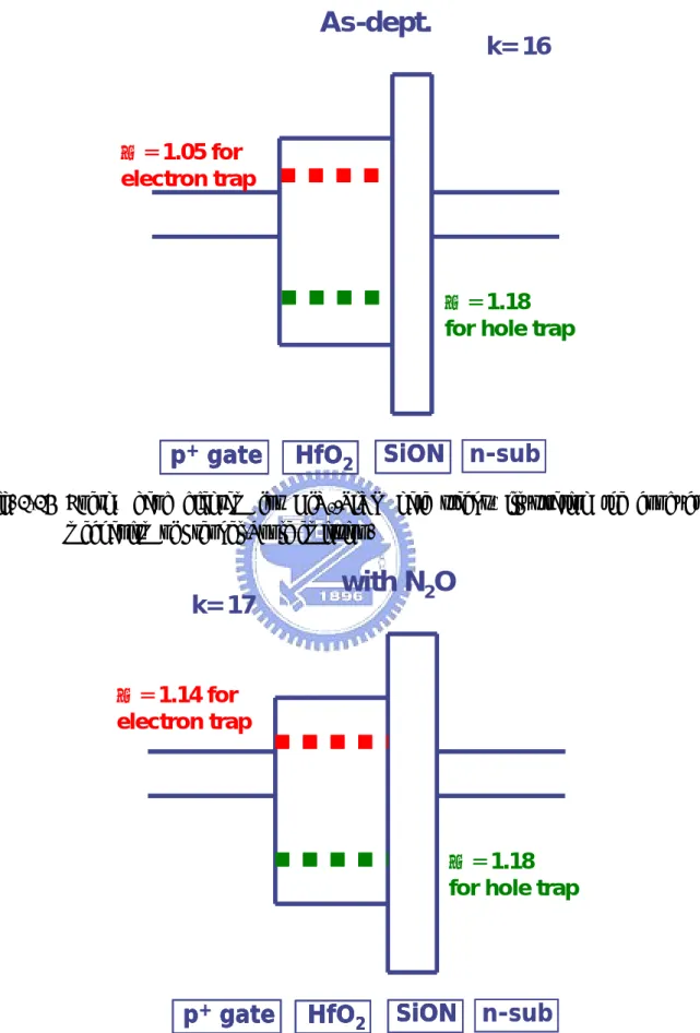
(32) height, E is the electric field in the HfO2 film, ε 0 is the free space permittivity, ε k is the dielectric constant of HfO2, k is Boltzmann constant, T is the temperature measured in Kelvin. ⎛J⎞ Excellent fitting curves are shown in the plot of ln ⎜ ⎟ versus E 0.5 of IG, indicating ⎝E⎠. that the conduction mechanisms both under gate and substrate injections for the SiON/HfO2 gate stacks, with and without post-N2O plasma treatment, are F-P type in nature. The barrier height Φ B and the dielectric constant ε k of SiON/HfO2 gate stacks can be calculated from the intercept of y axis and the slope of the fitting curves according to (2.6). The ε k value is found to be around 16 for the control sample and around 17 for the sample with N2O treatment. The value is very close to the estimated value from HRTEM image, which is 13.4 for control sample and 14.6 for the sample with N2O treatment. In the high-k gate dielectric, two current components could dominate the gate leakage current. Recalling from the carrier separation results, ISD current is mainly contributed by the carrier in the inversion layer, i.e., holes, while IB current is mainly contributed by the minority carrier in the gate electrode, i.e., electrons. Fig. 2-21 shows the F-P plot for the source/drain current in the inversion region. Fig. 2-22 shows the F-P plot for the substrate current in the inversion region. The solid lines are fitting curves for all temperatures. An excellent fitting can be obtained, indicating that the conduction mechanism for the high voltage ISD and IB are indeed Frenkel-Poole-type in nature. The fitting parameters for the hole and electron barrier heights are 1.17eV and 1.05eV, respectively, for the control sample. Results for post-N2O plasma samples are shown in Fig. 3-23 and Fig. 3-24. Again, good fitting curves can be seen, indicating that F-P is the right mechanism for both ISD and IB. The barrier heights are 1.14eV and 1.18eV for electrons and holes, respectively, for the N2O-treated sample. Note that the barrier height for electrons has changed from 1.05eV for the control to 1.14eV for the N2O-treated sample, indicating that the trap position has moved closer to the conduction band of the poly Si gate after post-N2O plasma treatment. The band diagrams are shown in Fig. 2-26 and Fig. 2-25 for the sample. 16.
(33) with and without post-N2O plasma treatment, respectively. The effective barrier heights for IG in the accumulation region are 1.389eV and 1.32eV for samples with and without N2O treatment, respectively.. 2.4 Summaries Improvements in the electrical characteristics of the p+-poly gate pMOSFETs with HfO2/SiON gate stacks by post-deposition N2O plasma treatments have been demonstrated in this work. We have found that improvements are achieved in many aspects, such as reduced leakage current, better subthreshold swing, enhanced normalized transconductance, and higher driving current. These improvements are ascribed to the lower interface states and bulk traps, as confirmed by various types of charge pumping measurement. Although charge pumping is a powerful technique to evaluate the interface state densities and bulk traps present in high-k films, care attention should be paid when dealing with dielectric that depicts larger gate leakage current, since the charge pumping current will be severely influenced in such case. Note that this phenomenon is entirely different for th nMOSFETs, where the leakage current will contribute to the source/drain current, but not the substrate current. In evaluation of the reliability, we found that the degradation caused by the voltage stress is dominated by the charge trapping in the bulk of HfO2 films, rather than interface state generation, irrespectively of whether post-N2O plasma treatment was performed or not. In addition, it was observed that the electron is the main trapped species during stressing for the N2O-treated samples, which is very different from the hole trapping observed in samples without post-N2O plasma treatment.. 17.
(34) Chapter 3 Impacts on the Reliability of HfO2/SiON Gate Stacks by Post-Deposition N2O Plasma Treatment 3.1 Introduction As CMOS devices are scaled aggressively into nanometer regime, SiO2 gate dielectric is approaching its physical limit; the intolerably huge leakage current caused by the direct quantum tunneling of carriers through the ultra-thin oxide. HfO2 is one of the most popular candidates among high-k materials to replace SiO2. Even though HfO2 films have been shown to be scalable down to below 1nm, there still exist several issues that need to be overcome. In this chapter, we focus on the study of reliabilities of the high-k dielectric, and address several topics including appropriate measurement setup, where the breakdown taking place (i.e., in the bulk or IL?), the behaviors observed in dynamic AC and NBTI stresses.. 3.2 Results and Discussion 3.2.1 Appropriate Measurement Setup for High-k Gate Dielectrics High-k materials, albeit slated as likely replacement for SiO2 in the future, do not possess the ideal quality for the gate dielectric as SiO2 uniquely does. During constant voltage stressing, the stressing has to be interrupted periodically in order to conduct Id-Vg and charge pumping measurements for determining the generated interface state density and the threshold voltage shift. As described in Chapter two, charge pumping measurement with fixed amplitude sweep is used to determine interface state density based on the recombination. 18.
(35) current measured by Icp at the substrate terminal. During measurement, pulse trains are applied to the gate electrode. However, this procedure is somewhat similar to the dynamic stress, and will cause extra degradation in the high-k films. In an attempt to more precisely single out the degradation caused by the constant voltage stress alone, it is necessary to pre-test the parameter setup, and make sure that no extra damage is done to the film. During the charge pumping measurement, the magnitude (∆VA) of every single pulse in the train has to be large enough to cause the recombination current. This means that the amplitude of the pulse has to exceed the flat band voltage and threshold voltage of the transistor. However, the amplitude should not be too large to avoid unnecessary stressing of the transistor during measurement. The Id-Vg measurement conditions also have to be carefully chosen in order not to cause similar unwanted effect. For high-k gate dielectric, there is a serious issue about Vth instability. It is shown that the magnitude of the Vth instability in the conventional MOSFETs with HfO2/SiON gate stack is strongly dependent on the details of the measurement sequence. It is believed that the origin of the Vth instability is caused by the fast charging and discharging of pre-existing defects near HfO2/SiON interface as well as in the bulk of the HfO2 layer. Therefore, conventional stressing and sensing experiments used to evaluate Vth stability can not fully qualify the film, because of fast de-trapping after stress, and it also means the Vth instability will be underestimated. Figs. 3-1 (a) and (b) show that the Id-Vg characteristic is dependent on the sweep direction, measurement sequence, and the minimum/maximum bias conditions. According to previous report [29], there is a defect band in the HfO2 layer located at an energy level above the Si conduction band edge. As the gate bias is varied, these defects have the possibility to rapidly trap and de-trap, causing Vth instability [29]. In Fig. 3-1 (a), we can see that after two successive sweep cycles of a Vg spanning between 0V ↔ -2V, hole trapping is observed. However, when the sweeping range of Vg is between 1V ↔ -2V, full recovery is obtained. This means that even with a very small voltage range, i.e., from 0V to -2V, 19.
(36) stress-induced effect can be detected, which could obviously lead to the misjudgment of threshold voltage shift. The situation is similar for the samples without N2O treatment that also exhibit hole trapping (Fig. 3-3 and Fig. 3-4). In order to discharge the charging of fast traps as much as possible, a small positive gate voltage (Vg=1V) is applied for 15 seconds, prior to the Id-Vg measurement as well as the charge pumping measurement, to minimize the fast unstable charge de-trapping effect during constant gate override stress.. 3.2.2 Breakdown Investigation by Carrier Separation Method Using the carrier separation measurement technique, we are able to distinguish two different. breakdown. mechanisms,. i.e.,. high-k. bulk-initiated. breakdown. and. an. interfacial-layer-initiated breakdown. The dielectric breakdown degradation is one of the most serious concerns in the high-k devices, whose characteristics are influenced by defects and fixed charges in the high-k films. Soft breakdown in high-k is unlike the one in SiO2, i.e., the soft breakdown current could be a critical issue in high-k for power consumption [32]. In the stacked high-k film like HfO2/SiON, attention should be paid to the fact that the electric field across the interfacial layer is larger than that across the high-k dielectric film. Since it is inevitable to form an IL layer when the high-k film was deposited on Si substrate, it is crucial to understand the relationship of leakage and breakdown in the HfO2/SiON gate stacks. Fig. 3-5 and Fig. 3-6 show that the absolute values of IG (gate current), IB (electron current), and ISD (hole current), as a function of gate voltage for a HfO2/SiON pMOSFET without N2O treatment. The dependence of ISD on the substrate bias is consistent with that of IG; meanwhile IB shows quite a different tendency. This means that the current collected at the gate electrode is mainly dominated by the inversion charge flow coming from the S/D regions; while the electron current injected from the gate electrode contributes to the substrate current. Recalling the carrier separation results in Chapter two, the gate leakage current is mainly contributed by the S/D current (IG+IB+ISD=0). As a result, IG will change with substrate bias, 20.
(37) indicating that IG also depends on the inversion charge concentration in the channel. Similarly, for the post-N2O plasma-treated sample; the S/D current is still dependent on the inversion charges in the channel, while the substrate current is not. Even so, the magnitude of the hole current is seen to be reduced significantly because of the increased interfacial layer thickness, and the electron current remains at the same order, as compared with the sample without post-plasma treatment. The evolution of IG, ISD, and the IB under negative constant voltage stress is shown in Fig. 3-8. The increment of IB is larger than that of ISD, indicating that the breakdown has taken place in the bulk. For more details, we interrupted the stressing three times to measure carrier separation currents during the stress, i.e., before the stress (Fresh), during the SILC condition, since SILC is generated during the interval, and after the soft breakdown (SBD). The results of IG, IB, and ISD of carrier separation are shown in Figs. 3-9 (a), (b), (c), correspondingly. Comparing Figs. 3-9 (b) and (c), the hole current is about an order larger than the electron current, as VG was swept from 0V to -3V at SILC condition. Moreover, the electron current is much larger than the hole current for |VG|<2V, indicating that dominant carriers are holes in SILC condition, and electrons in SBD. It can be reconfirmed in Fig. 3-9 (a) that IG=ISD in SILC condition, while IG=IB for SBD. In Figs. 3-9 (b) and (c), it is noticed that the increment in IB between Fresh and SILC is a little bit larger than ISD, implying that more electron traps are created than hole traps, resulting in an easier bulk-initiated breakdown after SBD. Further, considering the situation in SBD, we find that IB is much larger for the entire VG sweep from 0V to -3V. Therefore, we speculate that the electron path through the bulk after breakdown is as shown Fig. 3-9 (b). However, for ISD, the leakage increases rapidly as |VG|>|Vth| and becomes compatible with IB at |VG|>2.5V, indicating that the breakdown will be more likely to occur at the interfacial layer, due to the fact that holes have to tunnel through only IL at high voltage. The result is reexamined in Fig. 3-10. The same procedures were repeated to examine samples with post-N2O plasma treatment. 21.
(38) Fig. 3-11 shows the evolution of IG, IB, and ISD under the constant voltage stress of VG=-5.2V. Digital-like fluctuation is observed in SILC condition. Slightly larger increment in ISD than IB after SBD suggests that the breakdown path has formed nearer to the valence band of Si substrate, as shown in Fig.3-11. Carrier separation results of IG, IB, and ISD are shown in Figs. 3-12 (a), (b), (c), correspondingly. The gate leakage in SILC condition is dominated by ISD at high voltages, while in SBD the electron current is predominant. The increment for ISD between SILC and Fresh sample is larger than that of IB, indicating more hole traps were generated as compared with electron traps. After SBD occurrence, IG is mainly ruled by IB for the entire VG sweep range, which means that the breakdown path for the electrons has been formed. From Fig. 3-12 (c), we see an increased leakage even when |VG|<|Vth|, indicating a bulk breakdown. At even higher voltage above -2.5V, ISD is almost as large as IB, indicating that IL is also breakdown after the SBD. The result is reexamined in Fig. 3-13.. 3.2.3 Dynamic Stress For CMOS operation, VDD and GND signals are generally supplied to turn on and off the device, which means that AC gate bias is frequently used. However, in the reliability test of gate dielectric, DC stress is commonly used for convenience. The prediction from DC results in a unrealistically pessimistic device lifetime than AC. While AC stress gives a more realistic and correct insight into the device lifetime. It is reported that the threshold voltage shift is indeed reduced under dynamic stress in SiO2 [33]. Fig. 3-14 shows the schematic setup with several parameters for measuring threshold voltage instability of pMOSFETs under AC dynamic stress. For a fair comparison, the accumulated on-time is defined as the stress time. And duty cycle of 50% is used for all samples. The stress condition is at a gate overdrive Vgo=Vg-Vthc=-2.2V. First, we investigated the frequency dependence. From Fig. 3-15, it can be seen that generated Nit on the order of 1010 is quite independent of frequency. In contrast, the threshold 22.
(39) voltage shift shows strong frequency dependence. Under DC stress with Vgo=-2.2V, positive charges trapped in the gate dielectric are observed. On the other hand, under AC stress, trapped positive charges are reduced. Moreover, at the higher frequencies (larger than 10k Hz), negative charges, rather than positive charges, are being trapped, as shown in Fig. 3-16. This suggests that AC stress results in a reduced overall trapped density, rather than the generated interface state density. It is believed that de-trapping of trapped positive charges could happen during the off-time period. Also at higher frequencies, the observed negative charge trapping implies that the on-time is too short for positive charge trapping to occur in the pMOSFETs with HfO2/SiON gate dielectrics. Fig. 3-18 shows ∆Nit and ∆Ntot versus stress time, where ∆Ntot ≡. C × ∆Vthc . It illustrates that under DC stress, the threshold voltage shift is mainly q× A. controlled by charge trapping, whereas under AC stress generated interface state densities play a more important role. Next, the off-time characteristics (or reduced on-time for trapping carrier) were studied by verifying three duty cycles, i.e., 25%, 50%, 75%. Fig.3-19 shows that generated interface state densities are also independent of duty cycles. Fig. 3-21 shows ∆Vthc under AC stress with 100Hz and 10Hz. It is found that longer off-time de-traps more positive charges. Fig. 3-20 shows negative charge trapping under AC stress at a higher frequency of 10kHz. Because of the unipolar stress (i.e., Vgo=-2.2V during stressing cycle, Vg=0V during relaxation cycle), negative charges being trapped during off-time is unlikely to happen. Therefore, simultaneous trapping of positive and negative charges during on-time may be a reasonable explanation. In addition, the amount of de-trapped charges is greatly reduced at high frequency (10kHz), as compared to that at a low frequency (10Hz), indicating the on-time for trapping may be too short to trap holes. The same situation occurs for the post-N2O plasma samples, besides the trapping of negative charges under DC stress, i.e., de-trapping of positive charges during off-time (Fig. 3-23). Also, from Fig. 3-22 we further. 23.
(40) confirm that changing the frequency does not affect the generated interface state density for the samples with post-N2O treatment. Changing duty cycle has the same effect on the control samples for the threshold voltage shift and generated interface state density (Fig. 3-24 and 3-25).. 3.2.4 NBTI in HfO2/SiON Gate Stacks It is well-known that for the SiO2-based gate dielectrics, high voltage stress on the gate electrode of MOSFETs could change flatband or threshold voltage, in particular at elevated temperatures. This phenomenon is called bias temperature instability (BTI). Most of BTI researches on the SiO2 dielectric are focused on the negative BTI, because of aggravated degradation compare with positive BTI. Even more, Kimizuka et al. revealed that as the gate oxide thickness is scaled down to the range of 3.5nm, NBTI could become the bottleneck limitation to the SiO2 scaling than NMOS HCI [34]. NBTI of pMOSFETs is an important reliability issue for both digital and analog applications. Despite the many works on NBTI in order to keep NBTI at bay, including better modeling and improved processes, the basic rootcause mechanism is still not fully understood. Ogawa et al. proposed a model based on their experimental results [35]. Si3 ≡ SiH + p + ⇔ Si3 ≡ Si ∗ + H +. Reaction-limited. (3.1). Si3 ≡ SiH ⇔ Si3 ≡ Si ∗ + H i. Diffusion-limited. (3.2). O3 ≡ SiH + p + ⇔ O3 ≡ Si ∗ + H i. (3.3). ( H + , H i )interface ⇔ ( H + , H i ) bulk. (3.4). It can be seen that the model can be separated into reaction-limited and diffusion-limited processes. The reaction-limited is dependent on the number of holes near the interface available to interact with Si-H bonds. Once the reaction-limited processes are equilibrated, the diffusion-limited processes are dependent on the rate of diffusion of hydrogen away from the 24.
(41) interface. Figs. 3-25 (a) and (b) show Id, Gm-Vg characteristics before and after Vgo=-1.5V stress at room temperature and 125°C, respectively. A parallel shift of Id-Vg curve can be seen, and indicates that less △Nit is generated. Gm degradation is also alleviated. For confirmation, the generated interface state densities versus stress time are shown in Fig. 3-26. We can recall that the fresh Nit value is on the order of 8x10¹¹ /cm2, which means that the amount of △Nit is relatively small, compared to Nit. △Nit is shown to obey the power-law, and the index is 0.24, exactly the same value as that in the conventional SiO2, indicating that △Nit follows the reaction-diffusion model. Fig. 3-27 shows that △Vthc, increases with increasing temperature. The Dependence of △Nit and △Ntot on stress time is shown in Fig. 3-28. △Ntot is larger than △Nit by more than an order, indicating that the bulk traps in HfO2, rather than interface state. density generation, is responsible for the transistor degradation. After a gate overdrive stress of -2V for 1000 seconds at either room temperature or 125°C, the resultant Id, Gm-Vg are shown in Figs. 3-29 (a) and (b), respectively. We can see that Id depicts only a parallel shift after 1000 seconds stress, and Gm peak shows less than 5% degradation at room temperature. Similar trend is observed for the high temperature case. Subthreshold swing changes only slightly after stressing. As shown in Fig. 3-30, the generated interface state densities are degraded by the temperature stress as expected. According to the theory of NBTI, the threshold voltage shift (|△Vthc|) should keep increasing because of the increasing oxide traps. Unfortunately, it does not follow the predicted trend in our samples, as shown in Fig. 3-31. There are two possibilities: one is the increased electron trapping that compensates the hole trapping, and the other is the occurrence of recombination of the hole trapping. Fig. 3-32 clarifies the culprit of threshold voltage shift, whether it stems from the oxide traps or the interface states. At low temperature, △Ntot is about two orders larger than △Nit, indicating that trapping in the HfO2 bulk can be a very critical issue. However, Id. degradation curve in Fig. 3-33 reveals that the recombination of hole trapping is the root 25.
(42) cause of Fig. 3-31, as Id degradation should be worsen if the amount of total traps increases. The recombination occurrence can be explained by the rapidly increasing electron current as the temperature rises, while the hole current remains the same, as shown in Fig. 3-34. By changing the stress voltage to Vgo=-2.5V, a parallel shift is still obtained, as shown in Fig. 3-35 (a), and the subthreshold swing shows a slight increase after stress at 125℃. It is shown in Fig. 3-37 that trapping effect in high-k bulk is still an order larger than △Nit, indicating that reaction-reaction model may not be suitable for HfO2/SiON gate stacks, due to the preponderant bulk traps, compared to interface traps. As shown in Fig. 4-36, the index of power-law increases from 0.06 at low temperature to 0.15 at 125°C. This may be due to the fact that larger stress voltage causes the valence band of the Si substrate to shift closer to the hole trap, which is located at Φ B =1.17eV, as already mentioned in Chapter two, so holes become easier to jump and get trapped. Fig. 3-38 and Fig. 3-39 compare the control sample and the sample with N2O plasma treatment under Vgo=-2.5V 125℃. The improvement can be achieved after post-N2O plasma treatment, especially at high temperature. In conclusion, △Nit follows the reaction-diffusion model with a power-law index of 0.25, because our IL is still SiON. In addition, bulk traps always dominate the degradation of HfO2/SiON, which means that trapping effect is larger than hydrogen species effect. Fig. 3-40 shows that under dynamic stress, the recovery of △Nit is observed, and shows no dependence on the relaxation voltage. Fig. 3-41 shows that the trapping charges can be de-trapped by the relaxation voltage.. 3.3 Summaries Several kinds of reliability testing have been performed, such as dynamic stress, investigation of bulk or IL breakdown, and NBTI. It is found that post-N2O plasma treatment. 26.
(43) may not be beneficial because of the resulting higher electrons trapping under AC stress, even though it exhibits several advantages as discussed in Chapter two. Bias temperature instability shows that leakage current could affect the threshold voltage shift behavior. Our data also confirm that two different mechanisms exist in HfO2/SiON gate stacks, i.e., trapping and the NBTI. And the effect of trapping is larger than the reaction-diffusion effect.. 27.
(44) Chapter 4 Conclusion 4.1 Conclusion In the thesis, we performed the post-deposition N2O plasma nitridation to enrich the HfO2 film quality. Several important phenomena were observed and summarized as follows. First of all, Improvements in the electrical characteristics of the p+-poly gate pMOSFETs with HfO2/SiON gate stacks using post-deposition N2O plasma treatment have been demonstrated in this work. We have found that improvements include many aspects, such as reduced leakage current, better subthreshold swing, enhanced normalized transconductance, and higher driving current. These were ascribed to the lower interface states and bulk traps as confirmed by various types of charge pumping measurements. In the second part of the thesis, we have used carrier separation method to clarify the breakdown in HfO2 or IL. The behavior is different for samples with and without N2O plasma treatments. Finally, we have studied the dynamic stress and NBTI. △Vth is mainly caused by the trapping in the HfO2, rather than △Nit. Dynamic stressing enables us to have a more realistic and precise vision in the estimation of device reliability. And we found that the trapping effect is responsible for the transistor degradation. Under NBTI, we found that the trapping effect is larger than the reaction-diffusion model.. 28.
數據
![Fig. 1-3 Several high-k gate dielectric materials with their bandgaps and dielectric constants.[3]](https://thumb-ap.123doks.com/thumbv2/9libinfo/8442877.181971/50.892.137.767.118.999/fig-high-gate-dielectric-materials-bandgaps-dielectric-constants.webp)

+7
![Fig. 3-1 Repetitive Id-Vg traces for HfO 2 /SiON high-k gate dielectric using measurement sequence (a) [Vg=0V ↔ Vg=-2V], (b) [Vg=1V ↔ Vg=-2V]](https://thumb-ap.123doks.com/thumbv2/9libinfo/8442877.181971/71.892.126.684.118.1010/repetitive-traces-sion-gate-dielectric-using-measurement-sequence.webp)
![Fig. 3-2 Repetitive Id-Vg traces for HfO 2 /SiON high-k gate dielectric using measurement sequence of [1V, -2V], [1V, -2.2V], … , to [1V, -2.8V] (w/o post-N 2 O plasma treatment)](https://thumb-ap.123doks.com/thumbv2/9libinfo/8442877.181971/72.892.205.728.134.493/repetitive-traces-sion-dielectric-measurement-sequence-plasma-treatment.webp)
![Fig. 3-4 Repetitive Id-Vg traces for HfO 2 /SiON high-k gate dielectric using measurement sequence of [1V, -2V], [1V, -2.2V], … , to [1V, -2.8V]](https://thumb-ap.123doks.com/thumbv2/9libinfo/8442877.181971/74.892.203.737.142.512/repetitive-traces-sion-gate-dielectric-using-measurement-sequence.webp)

相關文件
雖然水是電中性分子,然其具正極區域(氫 原子)和負極區域(氧原子),因此 水是一種極 性溶劑
①尼古丁 ②焦油 ③一氧化碳
雙極性接面電晶體(bipolar junction transistor, BJT) 場效電晶體(field effect transistor, FET).
(Another example of close harmony is the four-bar unaccompanied vocal introduction to “Paperback Writer”, a somewhat later Beatles song.) Overall, Lennon’s and McCartney’s
在烘焙食品中,有三種主要的膨鬆氣體:蒸汽、空氣和二氧化碳。蒸汽(水蒸汽)是水的
探討燃燒所得的碳簇、活性碳及二氧化錳對 雙氧水分解的影響。將 3個100 mL量筒中各加 入 5 mL雙氧水和1 mL的清潔劑水溶液,分別 加入 0 .2 g碳黑、0.2
Estimated resident population by age and sex in statistical local areas, New South Wales, June 1990 (No. Canberra, Australian Capital
酸性氣體(二氧化硫、二氧化氮)可以飄浮到離源頭很遠的地
![HPSH [ 氧化數平衡反應式係數 ]](data:image/gif;base64,R0lGODlhAQABAIAAAP///wAAACH5BAEAAAAALAAAAAABAAEAAAICRAEAOw==)