國 立 交 通 大 學
電子工程學系 電子研究所
碩 士 論 文
奈米金氧半場效電晶體匹配特性之研究
Matching Properties of
Nanoscale MOSFETs
研 究 生: 周佳弘 Cha-Hon Chou
指導教授: 陳明哲 Prof. Ming-Jer Chen
奈米金氧半場效電晶體匹配特性之研究
Matching Properties of
Nanoscale MOSFETs
研 究 生: 周佳弘
Student:Cha-Hon Chou
指導教授:陳明哲博士
Advisor:Dr. Ming-Jer Chen
國 立 交 通 大 學
電子工程學系 電子研究所
碩 士 論 文
A Thesis
Submitted to Department of Electronics Engineering & Institute of Electronics College of Electrical and Computer Engineering
National Chiao Tung University in Partial Fulfillment of the Requirements
for the Degree of Master of Science
In
Electronics Engineering July 2008
Hsinchu, Taiwan, Republic of China
奈米金氧半場效電晶體匹配特性之研究
研究生:周佳弘
指導教授:陳明哲博士
國立交通大學 電子工程學系 電子研究所碩士班
摘要
本論文研究電路的不匹配效應與物理模型。首先針對背閘偏壓對於次臨界區 的影響,經由量測及分析不同尺寸並加以逆向及順向偏壓電晶體,觀察次臨界區 存在比過臨界區更大的電特性誤差,主要的原因在於次臨界區中,電流與閘極電 壓及製程參數成指數的關係影響所致,其中也發現電流誤差會隨著逆向偏壓的加 劇而增大,從另一個角度去思考,電流誤差會隨著背閘順向偏壓的增大而改善, 這樣的結果是由於閘控橫向電晶體低注入情況產生所致。同時我們亦推導出一個 新的解析式統計模型,並成功模擬在次臨界區對不同元件在不同偏壓下所量測的 結果,另外電流誤差也被表達成以製程參數變動為因子的函數,所萃取出的參數 變動值與元件面積平方根的倒數成正比,符合前人所提出的論點。 在接下來的過程中,我們利用已經萃取出來的參數做進一步的利用,並特別 探討臨界電壓的變異特性,過程中利用和別人的模型做比對,一方面探討背閘偏 壓對臨界電壓的影響,另一方面探討不同的汲極電壓下,所造成臨界電壓的差 異,此時導致電子能階產生變化,而使元件的控制力有所升降;在其中臨界電壓 變異也是探討的重點之一,如此一來便可發現元件匹配程度,並進一步得知電路 設計時的限制,並設計出電子電路最適操作情況。 中間過程中,因為通道尺寸的縮小,有些前人未考慮的因子必須被考慮, 如通道長度要考慮成有效的通道長度,因此在這個部份,利用 EDT 模型去求出 重疊長度部分,並藉此確認元件的有效通道尺寸;而另一個重要的物理因子,源極以及汲極的阻抗,則利用不同背閘偏壓情況下所產生的電流特性,並加以高的 電場,利用載子遷移率相同的特性而求出阻抗大小。 從一開始,我們探討元件操作在次臨界區域,並討論其中匹配特性,在最 後的步驟,我們探討了元件操作在過臨界區域匹配特性,並利用一套新的背向散 射理論推導出其相對應的變異模型,其中考慮到背向散射的原理,而使元件操作 在飽和區,再利用之前已經得到的參數臨界電壓、汲極電壓致使位障下降因子以 及新的萃取參數:背向散射係數,並加上考慮有效的通道長及源極和汲極的阻抗 來建構整個不匹配模型,當然也建立背向散射係數匹配模型,並加以運用在整個 電流誤差模型,也成功的達到預期中的結果。
Matching Properties of
Nanoscale MOSFETs
Student: Cha-Hon Chou
Advisor: Dr. Ming-Jer Chen
Department of Electronics Engineering
& Institute of Electronics
National Chiao Tung University
Abstract
This thesis investigates the current mismatch and derives a physical model. First, we have discussed the back-gate bias control on subthreshold circuit mismatch. We have measured the MOSFETs operated in subthreshold region with different gate widths and lengths. These MOSFETs were characterized with back-gate reverse and forward biases. We have observed that the devices operating in subthreshold region exhibited larger mismatch than those in above-threshold region. The is due to the exponential dependence of current on gate and bulk voltages as well as process variations. In the case of back-gate reverse bias, we have found that current mismatch increases as the magnitude of back-gate reverse bias increases. On the other hand, with the supply of back-gate forward bias, the current mismatch decreases with increasing the back-gate forward bias. The improvement in match is due to the gated lateral bipolar action in low level injection. We have also statistically derived an analytical model that has successfully reproduced the mismatch data in weak inversion for different back-gate biases and different device dimensions. With this model, the current mismatch can be expressed as a function of the variations in process parameters. The extracted variations are shown to follow the inverse square
root of the device area.
In the following work, we have used the results of extraction for different parameters. We also pay more attention to the threshold voltage fluctuation compared to different models. The substrate bias dependence of threshold voltage standard deviation was also discussed. On the other hand, we have found that drain voltage bias caused the effect of DIBL.
To reconfirm the reliability of our model, we have taken some parameters into account. In order to obtain the effective channel length, we have used the edge direct tunneling (EDT) model to gain the overlap length. On the other hand, the source/drain series resistance is also an important pole in our model. By incorporating the constant mobility criterion into the current equation under different bias conditions, the series resistance can be easily achieved.
In the beginning, we have discussed the devices operated in the subthreshold region. In the end, we have discussed the current mismatch in above-threshold regions and derived a physical model based on backscattering theory. Due to the backscattering theory, we have discussed the devices operated in saturation region. We have also derived a backscattering based mismatch model with key parameters, DIBL, threshold voltage, and backscattering coefficient. The effective channel length and series resistance were also taken into consideration to confirm the validity of the mismatch model. We have achieved that the backscattering coefficient mismatch model was feasible for our data. We have also successfully used the new mismatch model to reproduce the experimental current mismatch.
Acknowledgement
Cha-Hon, Chou July 2008 光陰轉眼即逝,回憶在交大的日子裡,有歡樂也有淚水,歡樂於實驗室同伴 的笑聲間,那過去的二年間,和一群同伴從不識到相識,有幾多愁盡付笑談中, 這是最快樂的時光 ; 淚水於驪歌的初唱,朋友們,與君一聚,終需別離,走在 金黃的斜陽下,漫步在六年如一日的道路上,夕陽照著臉頰,卻早以分不清是汗 水還是淚水,觸目著景色依舊,卻只能輕聲道句珍重再見。 二年間,過去的畫面不斷浮現於腦海,從陳明哲老師對學生的諄諄教誨, 一字一句皆對日後有著深深的啟發,研究的日子中,偶有迷途之意,所幸老師拉 了學生一把,讓學生有更廣的視野。 實驗室中的謝振宇學長,給予意見並相互 討論,對晚生有著前人經驗引之為鑑; 另外,李韋漢學長是研究此領域的先驅, 建立在其經驗上,使實驗進行的更順利; 而許智育學長則給予很多建議,這二 年在實驗室的日子中,或有挫折困頓之時,許學長總耐心聆聽著,也從中給予意 見;而李建志學長則是籃球場上也是生活上的好朋友,忍受後輩的無知,並從旁 扶持著學生。 同儕之情,更難以用文字表白,宋東壕同學是個值得信任的夥伴,有了這 樣的同學合作,事情往往事半而功倍;林以唐同學,在很多的日子裡,在漫漫長 夜裡,總會促膝長談著,與君一席話,勝讀數載寒窗;面對許多物理特性有所不 解時,梁惕華同學以其豐富的知識,從中解答疑惑; 至於呂立方同學,和學生 的交集從過去延伸到這些日子,沒有太多言語上的交談,但一切早已盡在不言中; 而陳彥銘同學,是個向上的青年,在籃球場上,眼神的交會就能意識彼此; 簡 鶴年同學,雖然彼此並無太多交集,卻也是個好同伴。 碩一的學弟,湯侑穎,在交大電子的六年中,從彼此陌生,到足球場上的 戰友,那日在台大球場上,奔馳於草地上,凜冽的寒風吹著,滂沱的大雨下著, 數度跌在泥沼之中,不及拭去身上的泥沙,旋即奮起追逐著,終有著奪冠時的榮 耀,那些日子,有笑有淚,那些回憶,歷歷在目,過往片段永遠難以忘懷,只可 惜一切只待追憶。另外陳又正也是個健談的學弟,同時也讓我增廣許多見聞;以 及努力向上的陳以東學弟,為了家計,非常辛苦。 最後要感謝的是我摯愛的母親和敬重的兄長,這一輩子,在數次失意的日 子中,母親總是給予安慰,人生之中有太多難以向外人所述之事,母親是唯一的 聆聽者,讓我從幾乎放棄再重新站了起來,母親,謝謝您這二十多年來無怨無悔, 這一生,已經了無遺憾; 而我的兄長,是這一輩子給予最大影響的人,我們兄 弟來自同樣的背景,有著相似的境遇,彼此相知相惜,有過同樣的挫敗,也曾有 著相同的夢,這一輩子即便一無所有,至少還有您和母親,這就夠了。 二十年前的風,二十年後依舊吹著,這段日子中,發生了太多事,也讓我 體會了人生中的冷暖,景物雖變,我心依舊。Contents
Chinese Abstract ... i
English Abstract ...iii
Acknowledgement ...v
Contents ... vi
Figure Captions ...viii
Chapter 1 Introduction...
1
1.1 An Overview for Measured Devices...1
1.2 Matching Properties of MOS Transistors ...2
1.3 Mismatch Model ...3
Chapter 2 Subthreshold Operation ...5
2.1 Basic Concepts about Subthreshold Operation...5
2.2 Experimental Subthreshold Operation...6
2.3 Subthreshold Mismatch Model ...6
2.4 Conclusion for Devices Operated in Subthreshold...9
Chapter 3Random Threshold Voltage Fluctuation...11
3.1 Fluctuation Model...11
3.2 Using Extraction of Mismatch CoefficientAγ and to Derive ...13
fb th V A AV 3.3 Effect of DIBL on Threshold Voltage ...15
Chapter 4 Extraction of Series Resistance and Overlap Length ...18
4.1 Constant Mobility Bias Conditions...18
4.2 Extraction of Source/Drain Series Resistance ... .19
4.3 Results and Discussion of Source/Drain Series Resistance... .20
4.4 Extraction of Gate-to-Source/Drain-Extension Overlap Length ...20
4.5 Results...21
Chapter 5 Mismatch in above Threshold Region...22
5.1 Backscattering Theory ...22
5.2 Analysis and Model...23
5.3 Devices Operated in above Threshold Region...24
5.4 Conclusion ...26
Chapter 6 Summary ...27
References ...28
Figure Captions
Fig.1 The drain current versus gate voltage characteristics with back-gate bias as parameter ………..31 Fig.2 Measured standard deviation versus the drain current divided by gate width to length ratio for zero back-gate bias.
………..32 Fig.3 The measured drain current mismatch in weak inversion versus the back-gate bias. ………..33 Fig.4. The normalized standard deviation versus the reference current measured from
different drawn gate width to length ratio with back-gate forward bias as parameter. ………..34
Fig.5 The measured standard deviation in weak inversion versus the back-gate bias. The calculated results from Eq.(9) are also shown for comparison.
………..35 Fig.6 The measured and calculated standard deviation of in the flat-band voltage difference versus the inverse square root of the device area.
………..36 Fig.7 The measured and calculated standard deviation of in the body effect coefficient difference versus the inverse square root of the device area.
………..37 Fig.8-1 Using Gm maximum method to determine Vth and constant current method to
determine the Vth1 and DIBL
………..38 Fig.8-2 Mean threshold voltage versus channel length for under different back-gate biases. ………..39
Fig.9 The measured and calculated standard deviation of in threshol d voltage difference versus the inverse square root of the device area.
………..40 Fig.10 Using measured data based on the fluctuation model to show the results under different back-gate bias.
………..41 Fig.11 The measured and calculated standard deviation of the difference in threshold voltage versus the inverse square root of the device area for different Vbs.
………..42 Fig.12-1 Fitting under different biases with respect to the results from Eq. (22).
th
th
V
A
………..43 Fig.12-2 AV versus Vbs from Eq.(22) for each size. Error stars stand for the standard deviation of the derivation.
………..44 Fig.13-1 Using constant subthreshold current method to determine the value of DIBL and threshold voltage at Vds=1V.
………..45 Fig.13-2 Extracted DIBL versus L for different channel widths.
………..46 Fig.13-3 Extracted threshold voltage versus L for Vds=1V.
………..47 Fig.14 The histograms of the measured Vth, DIBL and Vth1 for Vbs=0V
Fig.15 The measured and calculated square standard deviation of the difference in threshold voltage versus the inverse square root of the device area for Vds=1V.
………..49 Fig.16 The measured and derived standard deviation of the difference in threshold voltage
versus the inverse square root of the device area for Vds=1V.
………..50 Fig.17 Fitting under different biases from Eq. (26)
1
th
V
A
………..51 Fig.18 Extracted Rsd as a function of Vgs. Erroneous Rsd values appear in the low Vgs region ………..52 Fig.19 Experimental extraction of the edge direct tunneling current versus gate voltage. ………..53 Fig.20 Schematic illustration of channel backscattering theory.
………..54 Fig.21 A schematic flowchart for the procedure of extracting rc.
………..55 Fig.22 The experimentally extracted σDIBL versus the inverse square root of gate area. ………..56 Fig.23-1 The experimentally extracted σrc versus the inverse square root of gate area.
………..57 Fig.23-2 The experimentally extracted σrc versus the inverse effective gate length.
………..58 Fig.23-3 The experimentally extracted σrc versus 1
eff
L W
Fig.24 The measured drain current mismatch versus gate voltage derived from Eq.(42) and Eq. (46)
………..60 Fig.25 The measured drain current mismatch versus gate voltage from Eq.(43) and Eq. (45). ………..61 Fig.26 The measured drain current mismatch versus gate voltage derived from Eq.(44) and Eq. (45).
Chapter 1 Intoduction
1.1 Overview
It is well known that no two things are exactly the same in the world. The same situation can be applied to MOSFET: no two transistors can be the same due to the variation of manufacturing process. Matching property greatly influences circuit offset. Extensive studies on the matching behavior of devices have yielded a good understanding of the underlying physical phenomena and offer a designer quantitative model for the prediction of device performance variations [1]-[4]. In general, the designer can improve the matching of devices by increasing their area and this method will cause many disadvantages. If conservative transistor geometries are used, the consequence is a waste of area, while that also producing an increase in circuit capacitances. This may degrade the speed specifications and increase the circuit power consumption. However, using reduced transistor geometries produces large deviations in the transistor electrical parameters. This may render the circuits useless due to unexpected large variations of the circuit specifications. Thus, a precise mismatch characterization as a function of transistor area is necessary for optimizing the trade-offs between the area, speed, power consumption, noise and precision in circuit design. Some works on statistical characterization have been previously published in the literature [2]. These works deal with the do statistical characterization in the ohmic or saturation for the strong inversion region of operation. However, as low-power and low-voltage are becoming increasingly important specifications in analog design, the analog design is moving toward the moderate and weak inversion regions of the transistor operation. As a result, we generate different mismatch models for subthreshold region and above threshold region. The mismatch model for subthreshold region is based on subtreshold current mismatch model and mismatch model for above threshold region is based on backscattering theory.
In this work, a large number of statistical data then yield the standard deviation and mean of the distribution for random variables. For instance, we can obtain the fluctuation of the near-equilibrium threshold voltage, the drain-induced barrier lowering, etc. It can be found that threshold voltage mismatch follows inverse square root of area law and the corresponding size matching proportionality constant is quantitatively reasonable in comparison with those published thus far in the scaling direction. The DIBL, flat-band voltage and body effect coefficient mismatch still remain with such size dependence [4]-[6]. All the results would be revealed in the following work.
1.2 Matching Properties of MOS Transistors
When it comes to the caseoperation of MOSFET devices, the region of operations can be viewed as two conditions: above-threshold region and subthreshold region. In this situation, the devices operated in different regions are discussed individually and the models of different regions are based on different physical models. Mismatch is a limiting factor in general-purpose analog systems [1]. For the analog circuits, the operational region is mainly based on the above-threshold region. In digital circuits, matching can also be important in the write and read circuits of digital memories [2]. The impact of mismatching MOS transistors becomes more crucial due to the reduction of dimensions.
The operation of MOSFETs utilized the above-threshold region traditionally and the early papers about the mismatch of MOS devices were based on above-threshold region. We have extensively characterized MOSFETs in above-threshold region with different gate widths and lengths to determine the current mismatch. We have observed that the current mismatch decreases as the gate voltage increases. In the above threshold region, we have also derived a new model based on the backscattering model to derive current mismatch. Utilizing the parameters extracted from the data to build a new model can be valuable to verify the
accuracy of the backscattering theory.
In the subthreshold region, parameters for the mismatch will be different and the key points will be based on the flat-band voltage and body effect coefficient. Of course, some parameters will also be needed to complete the model. In this case, the substrate-to-source bias also plays an important role in the device mismatch. Since device characteristics depend on the back-gate bias, change of back-gate bias can cause different mismatch results. So we should take both the back-gate bias and device area into account at the same time.
1.3 Mismatch Model
Mismatch that can be observed between the parameters of a group of equally designed devices is the result of several random processes which occur during every fabrication phase of the devices. According to the citation [3], the standard deviation σf x y( , ) of a function f(x,y) with two random variables x and y can be expressed as
2 2 2 2 2 ( , ) ( ) ( ) 2( )( ) ( , f x y x y ov f f f f C x y x y x y σ ≅ ∂ σ + ∂ σ + ∂ ∂ ∂ ∂ ∂ ∂ ) (1)
where σx and σyare the variances of x and y, respectively; and the is the correlation coefficient between x and y. If the distribution f(x,y,z) is the function associated with three random variables x, y and z, the standard deviation of the distribution can also be presented in the similar way.
( , ) ov
C x y
Eq. (1) is the basic form for the establishment of the current mismatch, threshold mismatch, etc. As a result, we can make use of the phenomena to gain required results in the way. There we can argue that the correlation between different parameters may be an uncertain factor that could affect the results. Therefore, as the model is built we should make sure the existence of the relationship between different parameters. If no correlation between each other exists, we can get the simplest formula for the mismatch model. As a result, every time we want to build a new model we need to confirm the parameters to be independent or
not. Indeed, everything in this world may affect each other and may be viewed as a single event to another. Needless to say, the correlation coefficient may be negligible due to the low impact in our model.
Chapter 2 Subthreshold Operation
2.1 Basic Concepts about Subthreshold Operation
One of the fundamental factors limiting the accuracy of MOS circuits operated in the subthreshold region is the current mismatch. MOS dc mismatch has been discussed in the literature where a local-area mismatch model is frequently considered. And the variations of parameters in the processing of identically laid MOSFET’s result in dc circuit mismatch. There are many advantages for operating the MOSFETs in subthreshold region: low power dissipation, low-voltage swing and exponential dependence of drain current on gate-to-source voltage. Owing to exponential dependencies on the process variations, devices in the subthreshold usually exhibit a dramatically larger mismatch in current than that in above-threshold region. This poor control over the current match will cause undesirable effects in the circuit level.
In our experiment, there exists nonzero back-gate bias in the present of subthreshold MOS circuits [4]. In this situation, the dependence of current mismatch in weakly inverted MOS transistors is important. With respect to the well-known work concerning the mismatch analysis in the above-threshold, the study of mismatch in the subthreshold region is still limited. And the effect of back-gate bias on the mismatch is not discussed by previous paper in detail. In order to observe the current mismatch in subthreshold region, we should make sure that all the conditions are consistent in the extraction of the parameters.
The following issue will be focused on the back-gate bias. There always exists back-gate bias in the present processes. The back-gate bias has not received much attention in traditional circuit design. In this thesis, the back-gate forward bias has some advantages, such as improvement of matching property and increasing the transistor driving capability. The disadvantages due to back-gate forward bias will be demonstrated, which may be controlled by the strategies.
2.2 Experimental Subthreshold Operation
In this thesis, we used the capacitance-voltage(C-V) fitting to obtain the parameters as follows: gate oxide thickness=1.27nm, n+ polysilicon doping concentration=1*1020cm-3, and the substrate doping concentration =4*1017 cm-3. The devices under study were n-channel MOSFETs with varying gate widths (W=0.13μm, 0.24μm, 0.6μm, 1μm, and 10μm), and mask gate lengths (LMK=0.065μm, 0.1μm, 0.5μm, and 1μm), fabricated using a
state-of-the-art manufacturing process.
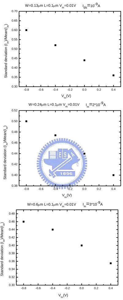
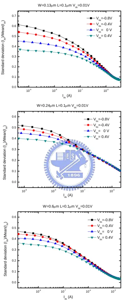
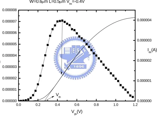
The measurement of the current mismatch for identical devices was achieved in terms of the dies on wafer. All dies on wafer contain many n-channel MOS transistors with the same structure. All the data were fabricated using a 65 nm CMOS process. The p-well-to-n+-source bias, Vbs, was fixed with the gate voltage sweeping from 0 V to 1.2 V in a step of 25 mV. Then we recorded and measured the drain current at the same time. All the procedure was performed under four different back-gate biases: -0.8 V, -0.4 V, 0 V, and 0.4 V [5]-[6]. And the drain voltage is fixed as high as 0.01 V in the subthreshold region. The measurement of the current mismatch in this study was achieved through the n-type MOSFET circuit.
The choice for the maximum forward bias is equal to 0.4 V in order to make sure of the action of the gated lateral bipolar transistors. The measured setup contained the HP4156B and a Faraday box was used for shielding the test wafer, all performed in an air-conditioned room with the temperature at 298K. Fig. 1 depicts typical measured I-V characteristic with back-gate bias as a parameter on a single n-channel MOSFET. We operated the MOS devices in the weak region [7].
2.3 Subthreshold Mismatch Model
voltage is below the threshold voltage, the drain current is based on the diffusion current. In this situation, the drain current is called the subthreshold current [6]:
2 2 exp( )[1 exp( )] 2 eff n Si a i s ds sub eff s a W kT q N n q I L q N kT kT μ ε φ φ ⎛ ⎞ ⎛ ⎞ = ⎜ ⎟ ⎜ ⎟ − ⎝ ⎠ ⎝ ⎠ qV − (2) 2 2 (2 ) exp[ ] i a n q kT N f φ = − (3) The following weak inversion current expression is considered for the derivation of the above model [4]:
2
( 2 )
exp( s) exp[ s f ] exp( gs th) i sub n n n a V V q q n I N kT kT nkT φ φ φ μ ⎛ ⎞ μ − μ − ∝ ⎜ ⎟ = = ⎝ ⎠ (4) Isub I0exp[Vgs Vth] nkT − = ; 0 exp( ) 2 2 1.5 f f bs q I kT V φ γ φ ∝ − − (5) where the critical voltage Vth =Vfb +1.5φf +γ 1.5φf −Vbs ; the Fermi
level f ( )ln( a i N kT q n φ = ) ; the slope 1 2 1.5 n V f bs γ φ = +
− ; and is the intrinsic concentration. From (1) the drain current I
i
n
sub can be written as a function of the variances in the associated process parameters
2 2 2 2 2 2 ( ) ( ) ( ) ( ) ds fb ds ds fb I V ds fb ds I I V I γ V I γ σ σ γ σ2 ∂ ∂ ≅ + ∂ ∂ (6) From (5) the derivatives in (6) can be obtained :
2 ( ) 1.5 1 2 1.5 gs th f bs ds ds f bs q V V q V I I nkT n kT V γ γ φ γ γ φ − − ∂ = − − ∂ − (7) fb ds fb ds fb V I qV I V nkT ∂ = − ∂ (8) The first and third terms of the right-hand side of (7) can not be neglected because the gate oxide thickness tox scales down and the channel effective doping concentration Na becomes large. Thus, we can obtain a mismatch model:
2 2 2 2 2 ( ) 1.5 [1 ] ( ) 2 1.5 ds fb gs th f bs fb I V f bs q V V q V qV nkT n kT V γ nkT γ γ φ σ σ φ − − ≅ − − + − σ (9)
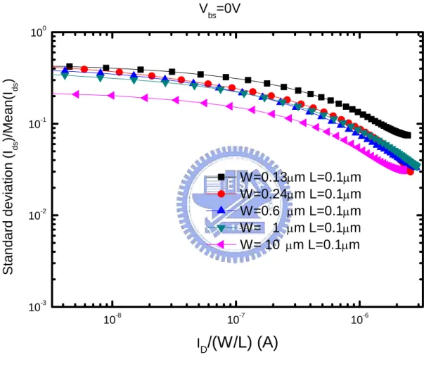
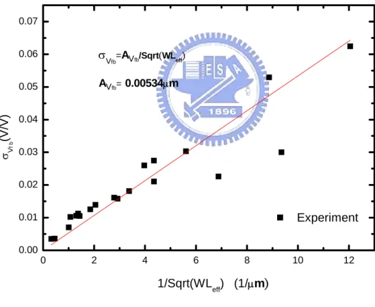
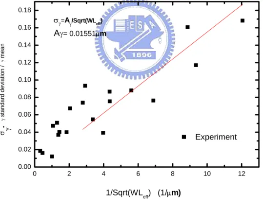
Fig. 2 shows experimental data in terms of
D
I
σ versus Ids/(W/L) for zero bias, where
W/L is the gate width to length ratio. Above formulation describes the dependence of
D
I σ on Vbs, realizing that the current mismatch increases with more negatively substrate bias Vbs. On the other hand, an increase in the forward bias Vbs can improve the transistor matching. So the current mismatch in weak inversion [8] [9] is a function of the standard deviation of the difference in Vfb and γ. And we can know that the weak inversion mismatch is independent of the current. Here we can use the constant current to determine Eq. (7) and Eq. (8), as well as the values of current mismatch. The results can be shown in Fig. 3. In order to get the results of size proportionality constants Aγ and , we need to calculate the
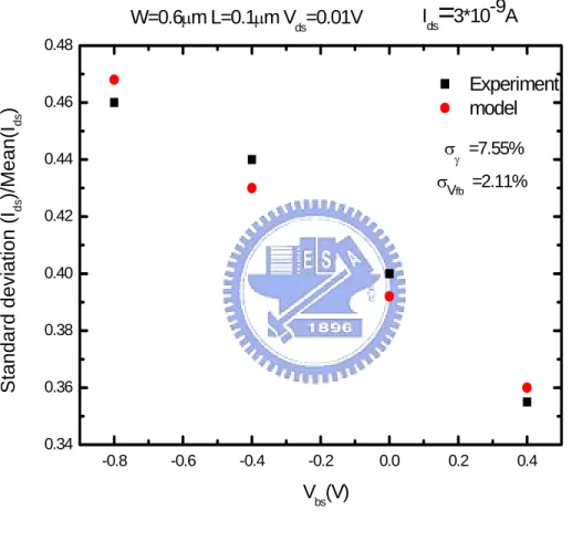
fb V A σγ and fb V σ for
each size. For instance, the calculated results based on Eq.(9) with σγ =7.55% and
fb
V
σ =2.11% have been found to be capable of appropriately reproducing the measured data as depicted in Fig. 5.
We concluded that the mismatch model for the subthreshold region can be affected by the back-gate bias and body effect coefficient. And we know that with the Vbs decreasing, the matching property would be gotten worse. This part can be proved from Fig. 4. Essentially, we assumed that the drain current mismatch will be different for different gate biases. The experimental results are useful for the circuits operated in the low power devices.
By substituting the gate oxide thickness, flat-band voltage and the doping concentration into Eq. (9), data from twenty ratios of different gate width to length in Fig. 4 have been reproduced over the back-gate forward bias range illustrated. The corresponding extracted variations in process parameters Vfb and γ versus the inverse square root of the device area are plotted in Fig. 6 and Fig. 7. Empirically, we have the formulas which follow
the inverse square root of the device area, in agreement with [2]. eff A WL γ γ σ = and fb fb V V eff A WL σ = (10)
where the Leff can be represented by the following formula
Leff =LMK − ΔL2 (11) In the above formula, we suggested that there will be the same LΔ at both ends of source and drain. Here LMK is the mask-level channel length. The value of LΔ will be extracted by the method of the edge direct tunneling and there LΔ will be called [10]. This part had been addressed in Chapter 4.
TN
L
Aγ and are the size proportionality constants for
fb
V
A σγ and
fb
V
σ , respectively. The extracted values of Aγ= 0.01551μm and =0.00534μm are shown in Fig. 6 and Fig. 7. Therefore, the combination of (9) and (10) can serve as an analytic design tool for properly calculating the mismatch with back-gate forward bias and device size both as input parameters. With the variation of different sizes, the parameters
fb
V
A
Aγ and
will be constants. To put it forward, this assumption can provide us with the characteristics in the circuits with the aim of designing a reasonable circuit with reasonable matching property [11] [12]. According to the results the safe region can be created for design guidelines.
fb
V
A
2.4 Conclusion for Devices Operated in Subthreshold
The on-chip n-type MOSFET circuits having different drawn gate width to length ratios with a large sample number ( 25) have been extensively measured over a small back-gate forward bias range. The MOS transistors with substrate-to-source junction slightly forward biased acts as a high gain gated lateral bipolar transistor in low level injection. Experiment has exhibited that the drain current mismatch occurs in weak inversion, especially for the
small size devices. An analytic mismatch model has been developed and has successfully reproduced the extensively measured data. The extracted variations in the underlying process parameters have been found to follow the inverse square root of the device area. The work of optimizing the trade-off between the match criterion and the device size with back-gate forward bias as design parameter has been demonstrated based on the model.
With the aid of this model, the current mismatch can be expressed as a function of the variations in process parameters, namely the flat-band voltage and body effect coefficient. The extracted variations are shown to follow the inverse square root of the device area. Examples have been given to demonstrate that the model is capable of serving as the quantitative design tool for the optimal design between the mismatch criterion and device size with the back-gate forward bias as a parameter.
Chapter 3 Random Threshold Voltage Fluctuation
3.1 Fluctuation Model
As MOSFETs are scaled down, the applied voltage is being steadily lowered to reduce the power consumption and keep the reasonable reliability. Therefore, we pay more attention to the fluctuation of the device characteristics due to the sensitivity of the systems [11]. In this work, we will repeat some work from the Takeuchi’s paper [13] and this method will pave a way for the future work. By the way, we make use of the data created in this work. Among the sources of the fluctuation, the random placement of impurity atoms is important [14], because it will cause substantial spread in threshold voltage. Of course, this problem cannot be eliminated by simply improving the process technology. And all the effects increase as the devices become smaller.
The vertical electric field in this model is a function of depth x in the channel region. A charge sheet is added within the channel depletion layer. The voltage drop between the surface and the depletion region is assumed to a constant. Hence, the relationship between threshold voltage and the charge sheet can be shown as a function of depth :
Q Δ x th (1 )( / ox) dep x V W Δ = − ΔQ C (12) Assuming that the impurity number distribution in the charge sheet volume is binomial, the standard deviation of QΔ will be
( ) sub eff N x x Q q L W Δ Δ = (13)
where the Nsub( ) is doping concentration. The standard deviation of the threshold voltage can be obtained by integrating the contributions of the charge sheets from =0 to =W
x x x dep. The result is ( ) 3 eff dep th ox eff N W q V C L W σ = (14)
where Neff is a weighted average of Nsub( ) defined as x 2 0 3 ( )(1 ) dep W eff sub dep dep x dx N N X W W =
∫
− (15) Threshold voltage formula is written as following :eff dep th fb s ox qN W V V C φ = + + (16) Substituting the formula (16) to (14), we can derive
( ) ( ) 3 ox th fb s th ox eff t V V q V L W φ σ ε − − = (17)
The coefficient BVth [9] can be introduced as below
( ) ox( th fb s) th Vth eff t V V V B L W φ σ = − − (18)
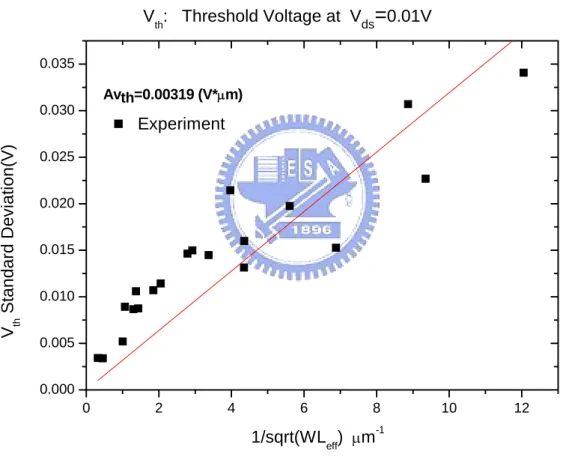
In this thesis, threshold voltage was obtained from gm maximum method and results are shown in Fig. 8-1 and Fig. 8-2. If (σ V )th is caused solely by ideal dopant fluctuation, BVth should be constant regardless of electrical gate oxide thickness and threshold voltage. In this part, we can gain the result from Fig. 10.
It is well known that standard deviation of Vth commonly satisfies the relationship
( ) Vth th eff A V WL σ = (19)
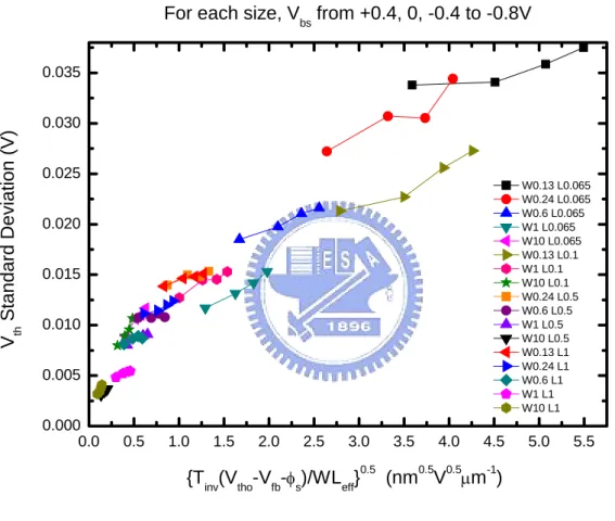
Due to the difference in the settings of Tox and Vth, AVth differs substantially. Results of Eq. (19) are shown in Fig. 9. However, the fluctuation model has offered an effective way to compare and analyze various kinds of transistors produced by different process conditions. On the other hand, the substrate bias dependence of threshold voltage standard deviation is also properly normalized based on the fluctuation model. In this case, the effects of the back-gate forward bias can be produced according to the fluctuation model and the trend agrees with our data. Fig. 11 shows that the size proportionality constant increases as reversal
bias increases in magnitude. This is well known for variance under change of back-gate bias and we will use this characteristic to complete the following work.
In the above statements, we assume that the threshold voltage fluctuation is based on the impurity in the channel region. In fact, the gate oxide thickness is also a significant factor in this model. In other words, as MOSFETs are scaled down to deep submicrometer feature size the intrinsic spreading in various parameters also plays an important part in the matching performance of supposedly identical transistors. Especially for the N-FETs, there are many possible mechanisms of variations. For example, flat band voltage variation, gate oxide thickness and extra factors will be an uncertainty in the model. However, we pay attention to the difference between Pelgrom’s model [2] and fluctuation model. This is the comparison on the behavior in the threshold voltage with the effect of back-gate bias taken into accout. The results are shown from Fig. 9 and Fig.10.
3.2 Using Extractions of Mismatch Coefficients Aγ and to Derive
fb th
V
A AV
It is a different aspect for us to understand the phenomena of the fluctuation of threshold
voltage [15]. We had known that the property of the threshold voltage fluctuation was discussed for many decades, and many people had tried a variety of methods to gain the model in order to obtain reasonable results. The fluctuation model is only an expression to alternationally understand another view for the variation of threshold voltage. Now we have another method to support the extracted values of the Aγ and . We will give attention to the details at the present time.
fb
V
A
First, the formula of threshold voltage can be derived as
Vth =Vfb +φs +γ φs −Vbs (20)
surface potential assumed to be equal to 1.5φf in this situation. A series of subthreshold data in Fig. 4 were transformed via Eq. (9) into the body effect coefficient mismatch σγ and flat-band voltage mismatch
fb
V
σ . Of course, we can observe all the effects for size proportionality constant for threshold voltage under different back-gate biases.
In the previous work, we applied the inverse square root of area law and obtained the proportionality constants Aγ and Therefore, we can make some assumptions according to the results such as to produce a physical model. Using the results of extraction for different parameters can bring interesting insights into observe the mismatch model. We can achieve good reproduction of data on the basis of our model.
. V
A
fb
Second, we will discuss the random threshold voltage fluctuation as well as the fluctuation mechanisms for the N-MOSFETs. The extractions of the threshold voltage and DIBL in each microscopically different transistors are carried out in the subthreshold at low drain voltages. On the other hand, in order to clarify the phenomena about the relationship between parameters, the results will be compared with the model adopted from the Takeuchi’s paper [5].
According to the work we had done, we can find that threshold voltage is also described by formula (1). Assuming that the correlation coefficient for the flat-band voltage and body effect coefficient is negligibly ignored, strikingly the following physically based relation remains valid: 2 2 2 2 2 2 (1.5 ) th fb fb f bs V V th th V V V 2 V γ γ φ σ = ∗σ + − ∗σ (21)
And we can simplify the above formula according to the proportionality constants ,
th
V
A Aγ
and . The proportionality constant can be written as
fb th 2 th fb V A AV 2 2 2 2 (1.5 ) V fb V f bs A =V A +γ ∗ φ −V A γ (22)
where the unit of is
th
V
A Viμmand the units of Aγ and are
fb
V
A μm. In this case, the effects of back-gate bias can also be observed. The results are shown in Fig. 12-1. We can find that as the reverse bias increases, the proportionality constant increases simultaneously. This result is reasonable according to formula (22) and we can achieve a new way to predict the influence of the bias.
th
V
A
When we employed almost all our time in research, something may be left behind in a hurry. To insure the reliability of our model, we can try another method to prove the relationship between parameters. As a result, an extraordinary fitting line between the measured and predicted variance is obtained for regions of operation and for a very wide range of transistor sizes, including minimum channel length transistors. In our point of review, this method is a new way to predict the proportionality constant , as shown in Fig. 12-2. That is, we only need to use a single sample to determine the , although we still need to gain the values of
th V A th V A
Aγ and . This is also a trivial process to attain the results. But we
have reached that this process is possible with different back-gate biases applied. This is the satisfying result along with assumptions consistent with the previous work.
fb
V
A
3.3 Effect of DIBL on Threshold Voltage
DIBL was defined as the threshold-voltage shift divided by the drain voltage change. In our case, DIBL can be expressed as follows
1 1 0 1 0 ( ) ( th ds th ds ds ds V V V v DIBL V V ) − = − − (23) where the form in our research is simplified to at the condition of drain voltage of 0.01V as usual. In Fig.13-1 and Fig. 13-3 the is extracted under V
0 ( th ds V v ) ) th V 1( 1 th ds V V ds=1V. In this
work, we employ a maximum trans-conductance method in the linear region to assess quasi-equilibrium threshold voltage as shown in Fig. 8 and the constant subthreshold current
method in the saturation region to extract the DIBL as shown in Fig. 13-1 and Fig. 13-2. Fig. 14 shows the histogram of the threshold voltage under different drain biases and DIBL. In the work, we will discuss the matching model for the DIBL and threshold voltage further. Simultaneously, we can write the formula as follows
Vth1(Vds1)=DIBL∗
(
Vds0 −Vds1)
+Vth(vds0) (24) According to Eq. (1), we can derive the mismatch model as follows(25) 1 th th 0 1 th 1 th th IBL th th 2 2 2 2 V v Vds DIBL σ =σ + Δ ∗σ
where . The results are shown in Fig. 15. We can see that the matching property of threshold voltage can be written as a function of DIBL and threshold voltage. In order to make most use of our data, we had better to retain the accuracy of our model. Therefore, we can simplify Eq. (25), leading to as below
1 ds ds ds V V V Δ = − V A 2 2 2 2 (26) V v ds D A = A + ΔV ∗A
where is determined by Eq. (22). In this work, we want to achieve a new method to simulate the value of size proportionality constants for the standard deviation of threshold voltage under V
V
A
ds=1 V. Indeed, we can observe that the results are expected as inferred from Fig. 16 and Fig. 17.
3.4 Conclusion
In this chapter, we discuss main parameters about threshold voltage and DIBL. We have compared the results between the fluctuation model and the traditional model. It is obvious that the fluctuation model can offer a way to see the changes in under different biases and manufacturing processes. Traditional model is still used to complete our model in the subsequent work. On the other hand, we can consider the effect of DIBL on the threshold
V
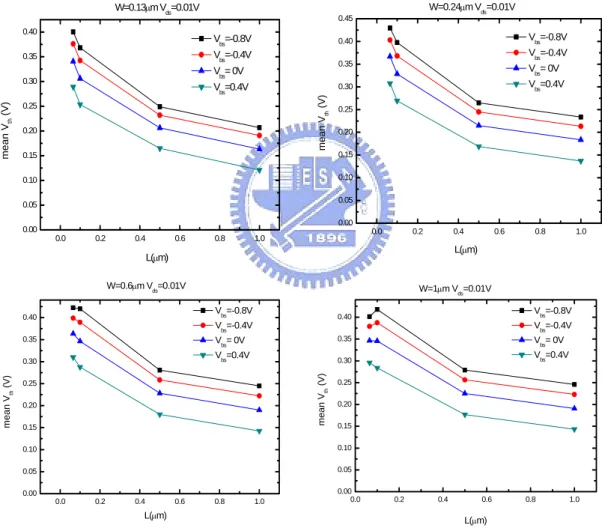
voltage. With channel length scaling down, it is gradually important to discuss short-channel effects such as roll-off of threshold voltage and drain-induced-barrier-lowering. Fig. 13-2 shows that DIBL increases dramatically as the channel length decreases. That is, we may not use the constant current method to determine value of DIBL and Vth1. The results may impose a problem as the gate length scales down to 50nm and beyond. Fig. 13-3 also shows the same obstacle as the channel length decreases. In such a condition, we can not extract the accurate Vth1. This phenomena is a big challenge needed to overcome.
Chapter 4 Extraction of Series Resistance and Overlap Length
4.1 Constant Mobility Bias Conditions
With the devices scaling down to the deep sub-micrometer region, some phenomenon and factors can’t be neglected for the transport property of semiconductor physics. In this chapter, we will introduce some factors that were neglected in the past and now will be taken into account due to the short channel effect. So we need to extract parameters as source/drain series resistance and the gate-to-source/drain-extension overlap length. This chapter is based on the factors of series resistance and the gate-to-source/drain-extension overlap length. These two factors really play dominant roles in our model are described below.
First, in order to build a new model, we should extract the value of source-and-drain series resistance. According to the result of the paper [16], a new model of extracting the MOSFET series resistance is cited. This method needs simple dc measurements on a single test device. Experimental demonstration is presented, and on the basis of the MOSFET equivalent circuit, the series resistance leads to excess potential drop, reducing the intrinsic voltage and degrading the drive capacity. As the gate length shrinks, the series resistance becomes a important factor of the total resistance. As the devices scale down, series resistance plays an important role in the circuits.
It is known that the use of previous methods is problematic, and this paper presents a mew method along with experimental demonstration and verification. We know that the relationship exists between the measured channel carrier mobility and the effective silicon vertical electrical field (Eeff) at the SiO2/Si interface [16]. The corresponding Eeff can be expressed as: eff 1 d 1 i Si E Q ε η ⎛ ⎞ = ⎜ + ⎝ Q ⎠⎟ (27) where εSi is the silicon permittivity, Qd is the depletion charge and Qi is the inversion layer
charge. η is an empirical factor with the values ~2 commonly used for electrons at room temperature. Based on the derivation procedure described elsewhere [17], Eq. (1) can be futher written as:
( 1) 2 3 gs th fb f eff ox V V V E t η η ηφ η + − − − ⎛ ⎞ = ⎜ ⎟ ⎝ ⎠ (28)
where Vfb is the flat-bandvoltage and φf is the potential difference between the Fermi level and the intrinsic Fermi level. Both Vfb and φf are essentially unchanged for a single device operated under different biases.
4.2 Extraction of Source/ Drain Series Resistance
By incorporating the constant mobility criterion into the current equation MOSFETs operated in the linear region, the results under different bias conditions are:
(
)
(
)
( 1) ( 1) ( 1) ( 1) ( 1) 0.5 bs bs bs bs bs V V OX eff V V d gs th ds ds eff C W I V V V V L μ = − − − V sd d R I (29)(
)
(
)
( 2) ( 2) ( 2) ( 2) ( 2) 0.5 bs bs bs bs bs V V OX eff V V d gs th ds ds eff C W I V V V V L μ = − − − V sd d R I (30)In this experiment, we assumed that the mobility is essentially the same under back-gate bias and considered mobility is the same under high Eeff condition.
( 1) ( 1) ( 2) ( 1) ( 1) ( 2) ( 1) ( 1) ( 2) ( 1) 0.5 0.5 ( ) bs bs bs bs bs bs bs bs bs V V V V V gs th th ds gs th ds ds sd V V d d V V V V V V V V R I I η η η ⎛ + − − − − − ⎞ =⎜⎜ − ⎟⎟ − ⎝ ⎠ VthV VthV (31)
In the above formula, the series resistance can be easily achieved. Fig. 18 shows satisfying results for the series resistance and a constant value about 220(Ω-μm) is determined for our model operated in above threshold region.
4.3 Results and Discussions of Extraction of Source/Drain Series Resistance
In order to obtain constant carrier mobility under different bias conditions, a sufficiently high Vgs is necessary to force the mobility to converge toward the universal curve. Then the extracted Rsd values approach constant and no dependency on the Vbs bias can be observed in the high Vgs region as depicted in Fig. 18.
Although the results of different sizes for extraction in the previous work will vary, we still view the results of the series resistant to be constant. This assumption is reasonable for the following model and the variation of series resistance only plays a minor role in the above threshold region. We can prove this by the results of mismatch model in the above threshold.
4.4 Extraction of Gate-to-Source/Drain-Extension Overlap Length
The edge direct tunneling (EDT) [10] of electron from n+ polysilicon to underlying n-type drain extension in off-state n-channel MOSFETs has ultrathin gate oxide thickness. It is found that for thinner oxide thickness, electron EDT is more pronounced over the conventional gate-induced-drain-leakage (GIDL), bulk band-to-band tunneling (BTBT), and gate-to-substrate tunneling. As a result, the induced gate and drain leakage and drain leakage is better measured per unit gate width. According to [10], an existing DT model readily reproduces EDT I-V consistently and the tunneling path size extracted falls adequately within the gate-to-drain overlap region. The ultimate oxide thickness limit due to EDT is projected as well.
In this work, we explored a dominant off-state leakage component via edge direct tunneling of electron from n+ polysilicon to underlying n-type drain extension for ultrathin gate oxide thickness. With the effective edge-tunneling area (= ), the EDT I-V model reads
IEDT =AQfT =L WQfTN T (32) where is the sheet charge of the accumulation layer; is the electron impact frequency on the n
Q f
+ -poly/SiO
2 interface; T is the modified transmission probability considering interface reflection factor. Finally, the extracted gate-to-source/drain overlapLTN is
EDT EDT TN I J L W = (33) In order to gain the value of the the gate-to-source/drain-extension overlap length, we had run a simulator to extract the value of the edge direct tunneling current density. In the pursuit of overlap length, we measured the edge direct tunneling current. Straightforward, the value of gate-to-source/drain-extension overlap length can be obtained. The tunneling path extracted was 6nm [18] ( ) wide from the gate edge as can be corroborated in Fig. 19. This is confirmed from the process simulation.
TN
L
4.5 Results
In order to confirm the validity of our model, we will take some parameters into consideration and think whether the results of our experiments are accurate or not. When we consider the effective channel length for the mismatch model, we will view the improved results, indicating a better condition than the past model that directly used the mask-level channel length. We will compare the results with those of other papers [18] to verify that the validity of hypotheses. Although the overlap length will be different for different sizes, we assume that an approximate value for LTN is reasonable.
Chapter 5 Mismatch in above Threshold Region
5.1 Backscattering Theory
In the backscattering theory, we use the wave concept to describe the carrier transport in the channel. As stated in backscattering theory [19]-[20], the nanoscale device performance is limited by the injection velocity and the backscattering coefficients. In this study, if the channel is under low electric field conditions, the width of the kBT layer calculated according to its definition is wide enough to be larger than the channel length L. The backscattering coefficient can be presented from
r low EC( eff) L
L λ
=
+ (34) where λ is the mean-free-path and L is the channel length. When the channel is under high electric field, <L, the backscattering coefficient can be estimated from
r high EC( eff)
λ =
+ (35) In our model, the channel is assumed to be operated under high electric field. In other words, we will discuss the devices operated in the saturation region. From Fig.20, we can derive the drain current easily and the drain current can be written
/ (36)
[ (0) (0)] [ (1 ) (1 ) qV kT] ds
I =W J+ −J− =qW F+ −R −F− −R e−
where R is the backscattering coefficient and T(=1-R) is the transmission coefficient. In the saturation region, the value of drain voltage will be higher than thermal voltage. So Eq. (36) can be modified as below
Ids =W J[ +(0)−J−(0)]=qWF+(1−rc) (37) where R=rc and substituting the F+ can be expressed
( ) (1 ) eff g th c C V V F q r + = − + (38)
Combining (37) and (38), we can derive the formula as follows ( ) 1 1 c ds eff g th inj c r I WC V V r υ − = − + (39) whereυinjare the thermal injection velocity at the top of source-channel junction barrier. In (39), the drain current is related to the backscattering coefficient[21]. In the mismatch model, we also can obtain the formula like Eq. (1) and Eq. (6). The mismatch model in above threshold region will be discussed later and we should characterize some parameters.
5.2 Analysis and Model
Based on backscattering theory, (39) is constructed except low drain voltage. Since the region is operated under high drain voltage. On the other hand, the main region for analog circuits is controlled in the saturation region. These two conditions will confine the region of our research. That is to say there will be some limitations when we extract the data.
In our research, there are several factors used to modify our model such as DIBL and Rsd. And Eq. (39) can be modified as follows:
( ) ( * ( * )) 1 1 c ds eff g ds s th d ds sd inj c r I WC V I R V DIBL V I R r υ − ⎡ ⎤ = ⎣ − − − − ⎦ + (40) Fig. 21 shows the flowchart for the procedure of extracting rc. Now we propose a new simple statistical model to quantitatively account for the above observed dependencies of the mismatch in the above threshold region on the gate-to-source bias. Eq. (40) the mismatch of the current,
ds
I
σ , can be derived as a function of the coefficients of variance of the parameters :
the coefficient of the variance in the threshold voltage,
th
V
σ , the coefficient of the variance in the drain-induced-barrier-lowering σDIBL, and the coefficient of the variance in the channel backscattering coefficient
c
r σ :
(
)
2 2 2 2 2 2 2 2 ( ) 4 (1 ) th c ds ds DIBL V c r I c gs th ds V r r V V DIBL V σ σ σ σ = ⎡⎣ Δ ∗ + ⎤⎦ − ⎡ − − ∗ ⎤ ⎣ ⎦ 2 + (41)In the above formula, we neglect the effect of source-and-drain series resistance. However, we will show the mismatch differences between models withand without Rsd.This new formulation describes the dependence of
ds I σ on Vgs. We calculate the c r σ under Vgs=1V
and Vbs=0V because the change of
c
r
σ with varying gate voltage in the above threshold voltage is very small. Fig. 24 shows that we use the backscattering mismatch model to reproduce the coefficient of the variance of drain current versus gate voltage over 0.4~0.5V at drain voltage of 1V. It can be found that the differences between the calculated results and experimentally extracted values are small.
5.3 Devices Operated in above Threshold Region
From the scatter plot of the measured near-equilibrium threshold voltage versus the reciprocal of the square root of the gate area at the mask level, we can see that a well known inverse square root of area law can apply:
th th V V eff A WL σ = (42)
The size law also remains effective for the DIBL case, as shown in Fig. 22. The physical origins of the underlying proportionality constants and can be connected to the statistical dopant fluctuation as stated previously.
th
V
A ADIBL
However, we can make sure that whether the backscattering coefficient mismatch data are able to be described by the size law or not. So we will list several cases to discuss the possible effects on the backscattering coefficient and hence determine the most fitting one in our research. First, we assume that rc mismatch obeys the size law:
c c r r eff A WL σ = (43)
The results can be shown in Fig. 23-1. Second, rc mismatch can be presented as being reversely proportional to effective gate length:
c c r r eff A L σ = (44)
The corresponding results are shown in Fig. 23-2. Finally, a new dimension dependent matching relationship is produced for the backscattering coefficient:
c c r r eff A L W σ = (45)
The results are shown in Fig. 23-3. In the above three conditions, we will compare the accuracy of each proposal model and then select a best one. It is a straightforward task to derive a backscattering-based mismatch version of Eq. (41):
(
)
(
)
2 2 2 2 2 2 2 2 ( ) 4 1 ( ) th ds c ds DIBL V c I r c gs th ds eff V A A r r V V DIBL V WL 2 σ = ⎡⎣ Δ ∗ + ⎤⎦ + σ ⎡ − − ∗ ⎤ ∗ − ⎣ ⎦ (46)In the above equation,
c
r
σ can be calculated by combining Eq. (43), Eq. (44) and Eq. (45). The results derived in Eq. (46) are shown in Fig. 24, Fig. 25 and Fig. 26 respectively. With the experimental means of the underlying random variables and known proportionality constants as input, the drain current mismatch was calculated using Eq. (46) and fairly reasonable agreements with the experimental data were achieved for the gate and drain voltages and effective mask gate lengths and widths under study. Obviously, as the gate length decreases the quantity of the rc term decreases through the enhanced carrier transmission across the channel.