行政院國家科學委員會專題研究計畫 成果報告
子計畫七:射頻頻率合成器與放大器晶片設計(3/3)
計畫類別: 整合型計畫 計畫編號: NSC92-2219-E-002-007- 執行期間: 92 年 08 月 01 日至 93 年 07 月 31 日 執行單位: 國立臺灣大學電機工程學系暨研究所 計畫主持人: 劉深淵 共同主持人: 楊清淵 報告類型: 完整報告 處理方式: 本計畫可公開查詢中 華 民 國 93 年 8 月 20 日
總計畫 :38-GHz 無線收發系統關鍵元組件技術(3/3) 子計畫七:射頻頻率合成器與放大器晶片設計(3/3) 計畫 編號:NSC 92-2219-E-002-007 執行期限:92年8月1日至93年7月31日 總計畫 主持人:王 暉教授 台灣大學電信工程研究所 子計畫主持人:劉深淵教授 台灣大學電機工程研究所 一、 中文摘要 由 於 個 人 通 訊 的 快 速 發 展 , 使 得 整 個 無 線 通 訊 產 業 蓬 勃 發 展 。 諸 如 下 一 代 的 數 位 網 路 : GSM、 CT2、 DECT 等 伴 隨 呼 叫 器 與 無 線 區 域 網 路 的 個 人 通 訊 系 統 , 亦 同 時 存 在 同 一 頻 段 。 數 據 通 訊 在 無 線 上 的 應 用 亦 為 世 界 各 國 所 積 極 發 展 的 一 個 課 題。同 時,更 高 頻 率 如 38GHz 之 微 波 射 頻 通 信 亦 是 將 來 的 通 信 寵 兒 。 此計劃將以 CMOS 之積體電路製程為主要 電路架構,建立主動與被動原件模型用以實現 跳頻式射頻頻率合成器與其控制電路、鎖相迴 路及除頻器電路,及射頻放大器並予以積體 化。最後進行積體電路之佈局及晶片製造,最 後測試並配合完成系統之整合。 本 計 劃 預 計 三 年 完 成 。 在 第 一 年 (90/8/1-91/7/31) 進行頻率合成器的探討與 電路架構的選擇。初步設計頻率合成器中之數 位電路部分。第二年(91/8/1-92/7/31)我們改 進螺旋電感特性,並應用於一頻率合成器。第 三年(92/8/1-93/7/31)我們 實現 一 5.2-GHz CMOS 低雜訊放大器。 英文摘要
Because of the fast development of the personal communication, it makes the whole wireless communication industry grow vigorously. Digital network that such as of future generation: GSM, CT2, DECT, etc.
follow the personal communication system of the calling out device and wireless regional network, also there is the same frequency band at the same time. It is also a subject of positive development of countries all over the world that the communication of the data is not having on-line application. Meanwhile, high frequency if microwave radio frequency of 38GHz it communicates to be communication pet in the future also. Plan this make with integrated circuit of CMOS Cheng main circuit structure, set up and take the initiative in order to realize jumping the frequency synthesizer and its control circuit, phase locking return circuit and except that device circuit frequently of radio frequency of the type frequently with the passive original paper model, and the radio frequency amplifier combines and accumulates the body. Overall arrangement and chip of carrying on the integrated circuit finally are made, test and cooperate with finishing systematic merger finally.
This plan is expected to finish in three years. Carry on the discussion of the frequency synthesizer and choice of the circuit structure in the first year (90/8/1-91/7/31). Design the digit circuit part in the frequency synthesizer tentatively. We improve the inductance characteristic of the
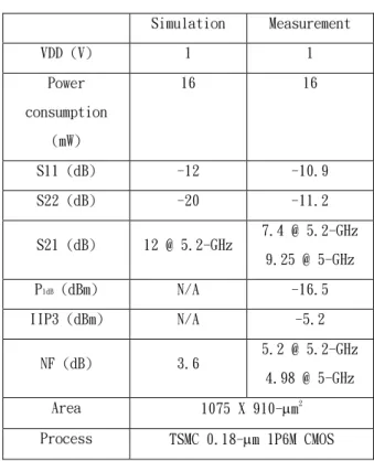
spiral in the second year (91/8/1-92/7/31), and apply to a frequency synthesizer. We realize one 5.2- GHz CMOS low miscellaneous news amplifier in the third year (92/8/1-93/7/31). 二、 計畫的緣由與目的 1. BiCMOS/CMOS 積體電路可工作於高頻數 位及類比電路,適用於本計畫之頻段。 2. CMOS 製程較其他製程便宜、整 合 性 高 且 台 灣 廠 商 擁 有 完 整 的 生 產 技 術 。 3. 積體化的電路,可降低成本、大小及功 率等的考量, 可提升其附加價值。 三、 研究方法及成果 第三年成果: 5.2-GHz CMOS 低雜訊放大器 CMOS LNA 的電路架構如圖 1 所示。 值得 注意的是 M2 的大小和 M1 不同。 這樣選擇電 晶體大小的主要原因是因為此 LNA 是在低電 壓下操作 ,僅僅只有 1 伏特的電源電壓。 因 此,為了使得電晶體在越小的 VDS下還能夠保 VDD Lg Ls M1 M2 M3 Input Output Ld1 Ld2 Vbias2 Rbias (2.5/0.18)-um X 32 (2.5/0.18)-um X 32 9.33 kohm 2.5 nH 0.6 nH 1.95 nH 1.9 nH (2.5/0.18)-um X 64 Fig.1 5.2-GHz CMOS 低雜訊放大器. Fig. 2. 5.2-GHz CMOS 低雜訊放大器佈局圖. 持在飽和區裡操作,我們需要使用更大的電晶 體尺寸。 這個電路是利用 TSMC 0.18 毫米 1P 6M CMOS 製程所製造,晶片圖如圖 2 所示。 一般的類比或數位應用的 pad 經常造成 極大的電容效應。 在 RF 頻率下,這些大的寄 生電容造成訊號顯著的損失和阻抗匹配的困 難. 為了解決這些問題,RF pads 已經被修改。 RF pads 由最高的金屬層 M6 以及最低的金屬層 M1 所組成, 並且利用 M1 層連接地作為屏蔽 層。 這種 pad 架構能降低寄生電容並且防止 雜訊從底層偶合造成干擾. 因為,我們在 RF 頻率範圍裡缺乏封裝模 型,加上封裝的寄生電感和電容會導致過多的 雜訊,我們利用在國家奈米設備實驗室(NDL) 內的 microprobe station 測試我們的裸片。 測試得到的 S11 和 S22 如圖 3 中所示,小於 -10dB。S21 和 NF50 如圖 4 所示。 功率增益 在 5.2GHz 有 7.4dB 並且有 5.2dB 的 NF50。 最 好的增益和 NF50 在 5GHz 時分別是 9.25dB 和 4.98dB。我們也測試了此 LNA 的線性度,如圖 5,以及圖 6 中所示,測試結果為-16.5dBm 的 P1dB 和-5.2dBm 的 IIP3。 上述的所有量測結 果是在 1V 電源電壓下,功率消耗為 16mW。 模 擬和量測結果之間的比較如表格 1 所示。 可能遭遇的困難: 1. 開發高頻的跳頻式頻率合成器積體電路
有相當的困難及挑戰性。 2. 全積體化鎖相迴路的設計與實現。各式積 體化電路的佈局與連線的考量。 3. 射頻元件特性不易掌握,缺乏精確的射頻 元件模型。 4. 測量設備與設計軟體之不足。 解決的途徑: 1. 正確地推導理論,選擇正確的方塊圖,利 用 CAD 軟體進行電路的模擬分析與設計, 配合晶片的製作,相互驗證。 2. 收集相關資料,加以分析與研讀。 3. 經由測試數據獲得精密之射頻元件模型。 4. 添購量測所需之儀器與相關 CAD 軟體。 量測成果: 4.6 4.8 5.0 5.2 5.4 5.6 5.8 6.0 6.2 -16 -15 -14 -13 -12 -11 -10 -9 -8 S11 & S2 2 ( d B ) Frequency (GHz) S11 S22
Fig. 3 Measured S11 and S22 of the LNA.
4.6 4.8 5.0 5.2 5.4 5.6 5.8 6.0 6.2 4.0 4.5 5.0 5.5 6.0 6.5 7.0 7.5 8.0 8.5 9.0 9.5 S21 & N F ( dB ) Frequency (GHz) S21 NF
Fig. 4 Measured S21 and NF50 of the LNA.
-26 -25 -24 -23 -22 -21 -20 -19 -18 -17 -16 -15 -14 -13 -4 -3 -2 -1 0 1 2 3 4 5 6 7 8 9 10 G ain ( d B ) Input Power (dBm) Gain
Fig. 5 Measured P1dB of the LNA.
-26 -24 -22 -20 -18 -16 -14 -12 -10 -8 -6 -4 -2 0 -60 -50 -40 -30 -20 -10 IM3 Fundamental Ou tp u t P o we r ( d Bm ) Input Power (dBm)
Fig. 6 Measured IIP3 of the LNA.
Table 1. LNA 模擬與量測結果比較 Simulation Measurement VDD (V) 1 1 Power consumption (mW) 16 16 S11 (dB) -12 -10.9 S22 (dB) -20 -11.2 S21 (dB) 12 @ 5.2-GHz 7.4 @ 5.2-GHz 9.25 @ 5-GHz P1dB (dBm) N/A -16.5 IIP3 (dBm) N/A -5.2 NF (dB) 3.6 5.2 @ 5.2-GHz 4.98 @ 5-GHz Area 1075 X 910-µm2 Process TSMC 0.18-µm 1P6M CMOS
四、 結論與討論 此一年(92~93)中,子計劃七按照規格設 計802.11b 接收機,其中頻率合成器部分已完 成晶片驗証。此計畫已獲得或預估之主要成就 與成果(output)(如論文篇、技術移轉經費/項 數、技術創新項數、技術服務項數、專利項數、 著作權項數等)如下表所列,其中重要論文也 於參考文獻列出[1~7]。已發表及投稿相關(含 會議)論文計 28 篇。其中包含 ISSCC 及 VLSI 各兩篇。 五、參考文獻
1. Weihsing Liu and Shen-Iuan Liu, "CMOS Tunable 1/x Circuit and its Applications", IEICE Trans. on Fundamentals, vol. E-86A, pp. 1896-1899, July 2003.
2. Chia-Hsin Wu, Chih-Chun Tang, Kun-Hsien Li and Shen-Iuan Liu, "CMOS 2.4-GHz receiver front end with area-efficient inductors and digitally calibrated 90° delay network", IEE Proceedings of Circuits, Devices and Systems, vol. 150, pp. 439-444, Oct. 2003.
3. Hsiang-Hui Chang, Chien-Hung Kuo, Ming-Huang Liu, and Shen-Iuan Liu, "A sub-1V fourth-order bandpass delta-sigma modulator", Journal of Analog Integrated Circuits and Signal Processings, vol. 37, pp. 179-189, Dec. 2003.
4. Chih-Hao Sun and Shen-Iuan Liu, "A Mixed-mode Synchronous Mirror Delay
Insensitive to Supply and Load
Variations", Journal of Analog
Integrated Circuits and Signal
Processings, vol. 39, pp. 75-80, April 2004.
5. Weihsing Liu, Shen-Iuan Liu and Shui-Ken Wei, "Low voltage and low power CMOS
exponential-control variable-gain
amplifier", IEICE Trans. on Fundamentals of Electronics. Communications and Computer Sciences, vol. E87-A, pp. 952-954, April 2004.
6. Weihsing Liu, Shen-Iuan Liu and Shui-Ken
We, "CMOS exponential-control
variable-gain amplifiers", IEE
Proceedings of Circuits, Devices and Systems, vol. 151, pp. 83-86, April 2004. 7. Ming-Huang Liu, Wei-Yang Ou, Tsung-Yi Su, Kuo-Chan Huang and Shen-Iuan Liu, "A low-voltage low-power 13-bit 16MSPS CMOS pipelined ADC", IEEE Journal of Solid-State Circuits, SC-39, pp. 834-836, May 2004. 表一 成果統計表 論文篇 年度 執行單位 計畫名稱 指標型 ISSCC 國 際會議 IEEE JSSC(IC 設計會議) 期刊論 文 會議論 文 其 他 專利項數 技術移 轉項數 專門技術數 公司營業 額 (百萬) FY91 台大電子所 射頻頻率合成器與放大器晶 片設計 0 2 0 5 FY92 台大電子所 射頻頻率合成器與放大器晶 片設計 1 4 0 4 FY93 台大電子所 射頻頻率合成器與放大器晶 片設計 1 3 7 1