行 政 院 國 家 科 學 委 員 會 補 助 專 題 研 究 計 畫
□成果報告
期 末 報 告
量子點太陽能電池之開發及應用 (3/3)
計畫類別: 個別型計畫 □ 整合型計畫
計畫編號:99-2119-M-009-004-MY3
執行期間:2010 年 8 月 1 日至 2013 年 7 月 31 日
計畫主持人:孫建文
共同主持人:
計畫參與人員:
成果報告類型(依經費核定清單規定繳交):□精簡報告 完整報告
本成果報告包括以下應繳交之附件:
□赴國外出差或研習心得報告一份
□赴大陸地區出差或研習心得報告一份
出席國際學術會議心得報告及發表之論文各一份
□國際合作研究計畫國外研究報告書一份
處理方式:除產學合作研究計畫、提升產業技術及人才培育研究計畫、
列管計畫及下列情形者外,得立即公開查詢
□涉及專利或其他智慧財產權,□一年□二年後可公開查詢
執行單位:
國立交通大學應用化學系
附件一中 華 民 國 102 年 10 月 3 日
Buried Quantum Dot Solar Cells for Terrestrial
Application
K.W. Sun
Department of Applied Chemistry, National Chiao Tung University E-mail: [email protected]
Introduction
This study is focus on the the colloids of Ba2SiO4:Eu2+ acted as luminescence down-shifting
centers in the ultraviolet region and the metallic nanoparticles also helped to enhance fluorescence in the visible region to increase light absorption and fabrication of PEDOT:PSS/Si hybrid solar cells. The content is divided into two parts:(1) metal-enhanced fluorescence in the visible region (2) surface nanostructured n-type Si and poly(3,4-ethylenedioxythiophene): poly(styrenesulfonate).
Part one: Eu2+-doped barium silicate (Ba2SiO4:Eu2+) nanophosphors dispersed in a
surfactant solution were spin-coated on commercially available silicon solar cells to form colloidal crystals on the surface. The crystals then act as luminescence down-shifting centers to generate low-energy photons for incident ultraviolet light. The fluorescence from the Ba2SiO4:Eu2+ nanophosphors was further enhanced by coating a metal-enhanced layer composed
of Ag nanoparticles and a SiO2 spacer. The solar cells showed an enhancement of0.86 mA/cm2
in short-circuit current density and approximately 0.64% increase in power conversion efficiency when coated with nanophosphors, SiO2 spacers, and Ag nanoparticles. The properties of cells
integrated with the metal-enhanced layer were characterized to identify the roles of nanophosphors and Ag nanoparticles in improved light harvesting. These experiments demonstrated that the colloids of Ba2SiO4:Eu2+ acted as luminescence down-shifting centers in
the ultraviolet region and the metallic nanoparticles also helped to enhance fluorescence in the visible region to increase light absorption within the measured spectral regime.
surface nanostructured n-type Si and poly(3,4-ethylenedioxythiophene): poly(styrenesulfonate). The Si surface before deposition of the organic layer was nanostructured by using CsCl self-assembled nanoparticles as a hard mask and dry etching to form radial junction architectures and enhance light diffusion and absorption. Apart from the textured Si surface, processing parameters such as from metal-electrode shadow ratio, spin-coating rate, and surfactant addition were properly adjusted to improve overall cell performance. Our hybrid solar cells achieve the best performance under optimized cell parameters with a power conversion efficiency of 8.84% and short-circuit current density of 30.5 mA/cm2. This combined technique provides a simple, scalable, and cost-effective process for fabricating hybrid solar cells.
Summary of major results
Part one:
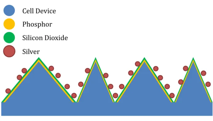
Figure 1 shows a schematic diagram of the synthesis of a micro-textured cell surface covered with nanophosphors, SiO2 dielectric layer, and Ag NPs (Ba2SiO4:Eu2+/SiO2/Ag NPs).
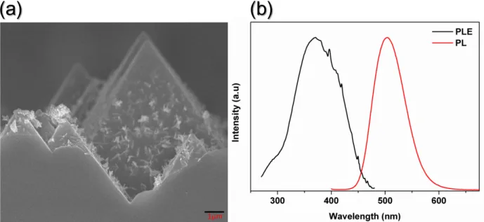
Figure 2(a) shows the scanning electron microscopy (SEM) image of the Ba2SiO4:7%Eu2+
nanophosphors. Figure 2(b) shows the photoluminescence excitation (PLE) and fluorescence spectra of the Ba2SiO4 nanophosphors in ethanol. The fluorescence spectrum showed a major
emission at 505 nm when the particles were excited at a wavelength of 350 nm. The PLE spectrum was measured at a fixed detection wavelength of 505 nm. The spectrum showed a broad resonance expansion from 300 nm to 450 nm with a peak centered at around 360 nm, indicating that the Ba2SiO4 nanophosphors exhibited the photon down-shifting by absorbing UV photons
Figures 4(a) and 4(b) show the EDS mapping results of a sample deposited with a 100 nm-thick SiO2 layer. The aforementioned Ag NPs dispersed in deionized water were then
spin-coated onto the SiO2 dielectric layers.
Figure 5 shows the down-shifted PL spectra excited at 396 nm of nanophosphors separated from the Ag NPs as a function of dielectric layer thicknesses. The PL intensity as a function of oxide thickness only is also shown in the inset of Figure 6. The spectrum of the nanophosphors without the metal-enhanced layer is also displayed for comparison. The enhancement in PL intensity strongly depended on the SiO2 layer thickness and reached the maximum at a thickness
value of 15 nm. The intensity considerably decreased with increased layer thickness of SiO2
The time-resolved spectra for the samples were obtained, and the PL decay times were determined. The decay times were plotted as a function of SiO2 layer thicknesses in Figure 6. At
the maximum PL enhancement, we extracted a decay time of 612.6 ns, which was much shorter than the case without the metal-enhanced layer. This result indicated that nearby Ag NPs can increase the intrinsic radiative decay rate of the nanophosphors, i.e., to modify the rate at which a nanophosphor emits photons. Our results suggested that the maximum fluorescence enhancement occurred at around 15 nm from the Ag NPs.
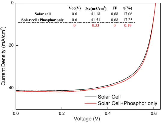
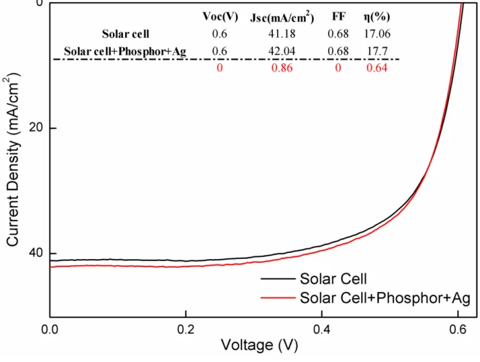
Figure 7 shows the J-V characteristics of the solar cell at the maximum enhancement. The performance of the cell without nanophosphors was also presented for comparison. Voc and FF
remained almost unaffected with increased Jsc from 41.18 mA/cm2 to 41.51 mA/cm2 with the
integrated nanophosphors. Therefore, the enhancement in cell efficiency can indeed be attributed to the increase in photocurrent and light absorption.
Subsequently, a series of solar cell samples was prepared and characterized at different preparation stages based on the structures in Figure 1 using an optimal concentration of 2 mg/ml Ba2SiO4 nanophosphor solution and SiO2 layer thicknesses of 10, 15, and 20 nm. The electrical
characterizations of these solar cells are summarized in Figure 8. The conversion efficiencies slightly increased when the cells were coated with nanophosphors only. The efficiency increased by nearly 0.7 % when the solar cell surface was covered with Ag NPs and a 20 nm SiO2 spacer.
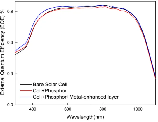
EQE measurements were performed to understand the mechanisms underlying the enhanced cell efficiency. The EQE of the c-Si solar cells prepared at maximum performance was measured relative to the bare cells without nanophosphors and metal-enhanced structures (Figure 9). The observed EQE enhancement between 500 nm and 600 nm is possibly due to increased lateral light scattering by the Ag nanoparticles, which tends to guide the light into directions that are then totally internally reflected. The presence of the nanophosphors clearly increased EQE in the UV, indicating that the increase in photocurrent was mostly due to the enhanced absorption of UV by nanophosphors. The EQE measurements agreed with the reflectance results, indicating that the cell response improved in the UV wavelength ranges because of the combined effects from LDS and PL enhancement by Ag NPs.
Figure 10 shows the J-V characteristics of the solar cell at maximum enhancement. The performance of the bare cell is also presented for comparison. The results showed that Voc and FF
remained almost unaffected with increased Jsc from 41.18 mA/cm2 to 42.04 mA/cm2 with the
integrated Ba2SiO4 nanophosphors and metal-enhanced layer. Therefore, the enhancement in cell
efficiency can indeed be attributed to the increase in photocurrent and light absorption. This finding agreed with the improved EQE (Figure 13).
Ba2SiO4 nanophosphors are LDS materials with a wide UV absorption band and a high
luminescent quantum efficiency (~ 40%). Thus, these nanophosphors can be used to achieve enhanced solar cell performance because they are low cost, easy to manufacture, and environmentally friendly. The Ba2SiO4 nanophosphors also do not undergo oxidation and thus
have higher stability for efficiency enhancement over solar cells coated with semiconductor quantum dots (QDs)/NPs, such as Si QDs.
Figure 8 shows the current-voltage (J-V) characteristic of the solar cell at maximum enhancement. The performance of the cell without the NHSL is also presented in parallel for comparison. The short-circuit current density (JSC), open-circuit voltage (VOC), fill factor (FF),
and conversion efficiency for the experiment cells are 43.5 mA/cm2, 0.56 V, 0.68, and 16.6 %, respectively, and for the reference cells, the values are 41.0 mA/cm2, 0.56 V, 0.67, and 15.6 %, respectively. VOC and FF remain almost unaffected as the JSC increases from 41.0 to 43.5 mA/cm2
with the NHSL on the textured surface. Therefore, the enhancement of cell efficiency is indeed attributable to the increase in photocurrent and light absorption.
Part Two:
A conjugated polymer called poly(3,4-ethylenedioxythiophene): poly(styrenesulfonate) (PEDOT:PSS) is the most widely used organic material for hybrid devices. PEDOT:PSS is transparent, conductive (1000 S/cm) and can produce a Schottky junction with Si.Illuminative light is absorbed in n-type Si, and a hole transport layer in PEDOT:PSS can extract holes generated in the Si substrate out of the device. Thus, the efficiency of the hybrid PEDOT:PSS/Si solar cell is comparable to a conventional Si p-n junction solar cell in principle. In this study, we demonstrate a hybrid solar cell that comprises a nanostructured n-type Si surface and PEDOT:PSS. The surface structure of Si was engineered by combining CsCl self-assembly and dry etching to form radial junction and antireflective architectures for light absorption enhancement.
The Si substrate after initial cleaning was dipped in dilute hydrofluoric (HF) acid (2%) to remove native SiO2. Immediately after HF cleaning and drying, a 100 nm thick Al layer was
deposited on the backside for cathode contact by using the sputter system. A highly conductive polymer solution was then prepared by mixing PEDOT:PSS (PH1000, Clevios) solution with 5 wt % dimethyl sulfoxide (DMSO) as a secondary dopant to increase conductivity. PEDOT:PSS was deposited onto the Si substrates by spin coating followed by thermal annealing at 120 °˚C for 10 min. Finally, the front anode contact was fabricated with a 60nm thick Ag grid by electron beam evaporation through a steel foil shadow mask.
To compare the performance of the hybrid solar cell with and without surface nanostructures, we first fabricated hybrid solar cells on a flat surface and optimized the efficiency with process parameters. The thickness of the organic PEDOT:PSS layer was controlled by the spin-coating rates. Under spin-coating rates of 1000, 3000, 5000, and 7000 rpm, the thicknesses of the PEDOT:PSS layer were 140, 70, 50, and 40 nm, respectively. Although the PEDOT:PSS layer is sufficiently conductive for forming a Schottky junction with Si and transporting light-generated holes out of the Si substrate; however, the conductivity of the PEDOT:PSS layer is insufficient as a top electrode. Therefore, we employed a finger-grid thin film of Ag as the top anode. Figure 1 shows the current density-voltage (J-V) characteristics of the devices with different front metal-electrode shadow ratios. The photocurrent of the solar cells was analyzed by using a solar simulator under air-mass 1.5 global (AM 1.5G) illumination conditions (100 mW/cm2, 25 °C). The three tested devices have the same electrode-finger width of 100 μm. The thickness of the PEDOT:PSS layer was set to 70 nm, which produced the best performance for all three devices. Devices with shadow ratios of 4%, 8%, and 18% were controlled by using different finger periods of 2, 1, and 0.5 mm, respectively. The short-circuit current density (Jsc) decreases when
the light absorption decreases with increasing shadow ratios. The fill factor (FF) improves from 54.9% (with a shadow ratio of 4%) to 61.9% (with a shadow ratio of 8%) and 69.1% (with a shadow ratio of 18%). The improvement in FF is attributed to the decrease in series resistance from 5.2 Ω·cm2
to 3.1 Ω·cm2
and 2.4 Ω·cm2
with increasing shadow ratios from 4% to 18%. The device with the highest top electrode density shows the best power conversion efficiency (PCE) of 6.59% because of improvements in carrier collection even though the Jsc decreases slightly. Therefore, all samples were fabricated by using top electrodes with shadow ratios of 18% throughout the experiment.
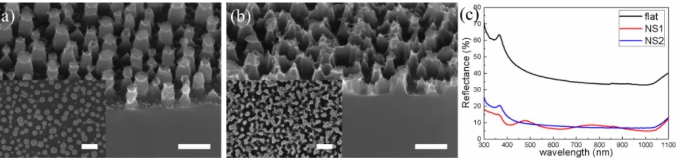
Nanostructures on the surface of the n-type Si substrate were fabricated by using CsCl self-assembly and dry etching. The Si substrate was then etched by RIE dry etching by using the CsCl islands as a hard mask. To achieve high light absorption and conformal polymer spin coating, the nanostructures on the Si surface should be smaller than the wavelength of incident light. The formation of a tapered nanostructure profile is prefered.The pillar structures, which is referred as the NS1 structure in this paper has a 100 nm to 200 nm diameter and 100 nm depth (scanning electron microscopy (SEM) image, Figure 2(a)). The reflectance spectra of the Si substrates with nanostructured surfaces were measured by using an UV/Visible/NIR spectrophotometer with an integrating sphere for 300 nm to 1100 nm wavelengths. Figure 2(c) compares the reflectance spectra of samples with nanostructured profiles and flat-surfaced Si substrates. The flat-surfaced Si substrate shows a reflection above 30% throughout the entire spectra. The NS1 nanostructure reduces the reflectance by approximately 25% to 40%; the reflectance is lower than 10% for wavelength longer than 450 nm. The average reflectance of the NS1 structure at a wavelength range of 300 nm to 1100 nm is 8.5%, which is lower than the flat-surfaced Si substrate (39.5%). The NS1 structure provides antireflective and light trapping effects to reduce the surface reflection and increase the absorption of the Si substrate.
Figure 3 shows the J-V characteristics of the devices with different spin-coating rates of PEDOT:PSS in the NS1 structure. Jsc was enhanced to above 25 mA/cm
2
because of increased light absorption compared with samples without nanostructures. However, the open-circuit voltage (Voc) and FF of these devices decrease compared with flat-surfaced devices. The decrease
of Voc is attributed to the increasing interface area and void between the polymer and Si, thus
leading to increased surface recombination.13,14,17
The lower FF is caused by the non-uniform polymer coating with voids and surface defects (Figure 2(a)). The best PCE performance of devices with NS1 surface structures is only 5.21%, which is lower than that of flat-surfaced samples. This result is caused by the deterioration of FF (54.9%) and Voc (373 mV) even with
increasing Jsc (25.4 mA/cm2
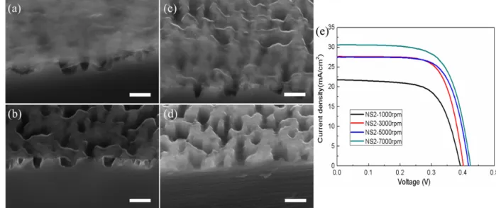
We used spin coating with different speeds to deposit the polymer and adjust the PEDOT:PSS/Si interface. Figures 4(a) to 4(d) show the SEM images of the PEDOT:PSS morphology coated on the surface of the NS2 structure at speeds of 1000, 3000, 5000, and 7000 rpm. Under a low spin-coating rate, the polymer formed a flat thin film with numerous voids between the polymer and Si (Figure 4(a)). The surface coverage of the polymer improves with increasing spin-coating rate. We were able to deposit the most conformal polymer film over the Si nanostructure under a spin-coating rate of 7000 rpm (Figure 4(d)). Figure 4(e) shows the J-V characteristics of the four devices with different spin-coating rates. Under the slowest speed, the device shows the lowest Voc (391 mV) because the polymer is unable to fully infiltrate into the
space between the Si nanostructures and form a continuous junction, thus leading to increased carrier recombination. Furthermore, the top surface is now smoother, thus reducing the antireflective effect. Jsc reaches 21.8 mA/cm2, which is a slight increase compared with that of
flat-surface device. The PCE was only 5.60%, which is lower than devices without surface nanostructures. The performance of solar cells gradually improves with increasing spin-coating rates. For devices at 3000 and 5000 rpm, Voc increases to 401 mV and 417 mV, respectively. Jsc
increases above 27.5 mA/cm2 because of the significant improvements in surface properties. The device fabricated at a spin-coating rate of 7000 rpm shows the most conformal surface morphology and provides the best results with Voc at 424 mV, Jsc at 30.6 mA/cm2, and PCE at
8.70%. The FFs of all four devices are within a close range (65% to 70%), which is similar to devices without nanostructures. This result indicates that the parameters used for processing the NS2 structure are optimal for processing highly efficient hybrid solar cells.
Figure 5(a) shows the measured external quantum efficiency (EQE) spectra of the hybrid solar cells fabricated with spin-coating rates of 3000, 5000, and 7000 rpm by using the NS2 surface structure. A device built on a flat surface with a spin-coating rate of 3000 rpm is displayed in parallel for comparison. The flat-surfaced device shows a maximum EQE of 68% at 440 nm.To make our argument more clear, the optical reflectance spectra of the nanostructured and flat surface Si after coating with the PEDOT:PSS are shown in Figure 5(b). When comparing the EQE and reflectance spectra side by side, it is clear that antireflection effect indeed is the predominant reason for the EQE enhancement. The device made at the spin-coating rate of 7000 rpm achieves the most conformal morphology, exhibiting an EQE above 70% over a wide wavelength range (i.e. between 400 and 850 nm). This particular device also displays the lowest reflectance throughout the entire wavelength range (Figure 5 (b)). In Figure 5(c) we show the enhancement ratios in EQE and light absorption between the flat device and device made at a spin-coating rate of 7000 rpm. Note that the enhancement ratio in EQE is significantly higher than that of the light absorption at longer wavelengths. This indicates that the efficiency improvement is not only due to antireflective effect but also attributed to higher carrier collection efficiency at longer wavelengths. The enhanced carrier collection efficiency at long wavelength can be explained by the following reason. The scattering from the surface nanostructures increases the optical path length inside the silicon and also makes the light propagate laterally. This results to the enhanced absorption of long wavelength photons near the surface (light trapping effect) than that of the flat surface.
Figure 6 shows the J-V characteristics of the two devices that have additional spin-coatings of 1% and 0.5% Triton X-100 at 7000 rpm before PEDOT:PSS deposition. Compared with a device without a wetting agent, the Jsc of the devices with wetting agents are
the FF was slightly reduce due to the nonconductive material involve resulting higher resistance. The PCE of the device treated with a 0.5% Triton X-100 wetting agent further improves from 8.70% to 8.84%.
We summarize the performances of devices made on NS2 structures and a flat surface in Table 1. Our best results show an increase in Jsc and the conversion efficiency by 58% and 34.1%
(from 6.59% to 8.84%) with optimized solar cell structures. We believe that improvements in Voc
by using better metal contact and reducing surface recombination can advance the performance of polymer/silicon hybrid solar cells further.
Nanostructures created by using CsCl self-assembly and dry-etching not only have the general advantages of self-assembly such as low cost and high throughput where an entire wafer can be patterned at a time, but also possess unique superior qualities: wide tunable/controllable
range of diameter and spacing by varying film thickness, relative humidity, and developing time. Furthermore, CsCl can be easily removed with water so that it does not leave behind any contaminants. Other than that, surface nanostructures cause high light absorption; thus, the device requires only a thin Si substrate, which can further reduce the cost of the solar cells. This combined technique provides a simple, scalable, and cost-effective process for the fabrication of efficient hybrid solar cells.