The novel precleaning treatment for selective tungsten chemical
vapor deposition
T.C. Chang
a, b,*, Y.S. Mor
c, P.T. Liu
c, S.M. Sze
a, c, Y.L. Yang
a, M.S. Tsai
a, C.Y. Chang
caNational Nano Device Laboratory, 1001-1 Ta-Hsueh Rd., HsinChu 300, Taiwan bDepartment of Physics, National Sun Yat-Sen University, Taiwan
cDepartment of Electronics Engineering and Institute of Electronics, National ChiaoTung University, 1001 Ta-Hsueh Rd., HsinChu 300, Taiwan
Abstract
The new solutions, hydroxylamine sulfate [(NH2OH)2H2SO4] combined with CuSO4, for cleaning Al via were investigated. It is found that the cleaning capability of hydroxylamine sulfate combined with CuSO4is better than that of hydroxylamine sulfate. Low via resistance of electrical test structure is obtained if the via is cleaned by this new cleaning solution. The hydroxylamine sulfate can ef®ciently remove Al3O2 and leave the clean Al on the surface of via. Then, the Cu ion in this new solution will immediately react with clean Al and form a copper passivating layer on the surface of via. The copper is more stable than aluminum in the environment and hard to be oxidized. Therefore, hydroxylamine sulfate combined with CuSO4can provide excellent cleaning capability for aluminum via holes. Also, the clean surface on the bottom of via is helpful for tungsten nucleation in via during CVD-W deposition. Therefore, a low via resistance and good selectivity of tungsten plug are obtained when the Al via is precleaned with this new solution. q 1999 Elsevier Science S.A. All rights reserved.
Keywords: Precleaning; Selective CVD-W; Hydroxylamine sulfate; Passivation
1. Introduction
In ultralarge scale integration (ULSI) technology, the multilevel interconnection is a key process. It is dif®cult to clean the bottom of via holes in the multilevel intercon-nection. If the bottom is not very clean, the performance and yield of IC will be degraded. Selective tungsten chemical vapor deposition (CVD-W) is one of the most attractive techniques for ®lling deep submicron via holes for ULSI applications [1±3]. Control of the deposition selectivity is essential for the successful selective CVD-W. The deposi-tion selectivity of CVD-W is very sensitive to the condideposi-tion of the via hole bottoms. If the bottoms are not clean, the local loss of selectivity called `creep-up' [4] will occur during the subsequent selective CVD-W. Creep-up is a phenomenon where tungsten growth starts not only from the bottoms but also from the sidewalls of via holes. Conventionally, the in-situ plasma sputtering [5±7] and reactive ion etching (RIE) have been employed extensively to remove the native metal oxide prior to tungsten deposi-tion. During the plasma etching, however, the outsputtered aluminum oxide and aluminum atoms can redeposit on the sidewalls of via and on the surface of dielectric layer, where
tungsten nucleation is induced, resulting in creep-up and selectivity loss during the subsequent selective CVD-W. In this work, we developed a simple and ef®cient preclean-ing solution, hydroxylamine sulfate ((NH2OH)2H2SO4)
mixed with CuSO4, to remove Al native oxide in the Al
via. Electrical characterization measurements have been performed to evaluate the effect of this solution.
2. Experimental
Aluminum alloy (Al±0.5%Cu) and antire¯ection layer (ARL) of TiN were sputter-deposited sequentially on ther-mally oxidized silicon wafer. The sample with TiN/AlCu bilayer was patterned by Cl2/BCl3-based RIE and
subse-quently covered with a dielectric layer of 1000 nm PECVD oxide. Via holes were patterned using the conven-tional photolithographic and dry etching technique.
Prior to the deposition of selective CVD-W, the wafers were treated with various precleaning processes for remov-ing the metal oxide on the bottoms of Al via. In this experi-ment, four types of samples were prepared. Sample A was treated with in-situ BCl3 plasma precleaning in the CVD
system. In this work, the predeposition plasma cleaning was conducted with a RF power of around 50 W, a BCl3
¯ow-rate of 100 sccm, and a chamber pressure of 6 mTorr. A post plasma-etching annealing at 3708C for 180 s was
0040-6090/99/$ - see front matter q 1999 Elsevier Science S.A. All rights reserved. PII: S0040-6090(99)00549-0
www.elsevier.com/locate/tsf
* Corresponding author. Tel.:1886-3-527-6100; fax:1886-3-572-2715. E-mail address: [email protected] (T.C. Chang)
performed to eliminate such by-products as AlCl3from the
aluminum surface. The wafers were then transferred from the plasma-etching chamber to the deposition chamber without exposing to atmosphere. The base pressure of the CVD chamber was 1026Torr.
Sample B was dipped in diluted solution of hydroxyla-mine sulfate with a concentration of 0.1 M for 1 min at a temperature of 508C.
Sample C was treated with two-step cleaning. First, the wafers were dipped in diluted solution of hydroxylamine
sulfate with a concentration of 0.1 M for 1 min at a tempera-ture of 508C. Secondly, the wafers were sequentially dipped in 0.1 M CuSO4solution for 1 min at 608C.
Sample D was dipped in mixed solution of 0.1 M hydro-xylamine sulfate and 0.1 M CuSO4for 1 min at a
tempera-ture of 508C. Then, samples B, C and D were sequentially loaded to the load-lock cold-wall CVD-W system within 5 min and selective CVD-W was deposited. In this work, the typical process conditions for the selective CVD-W were as follows: substrate temperature 3008C, total gas pressure 100 mTorr, WF6¯ow-rate 20 sccm, SiH4¯ow-rate 6 sccm, H2
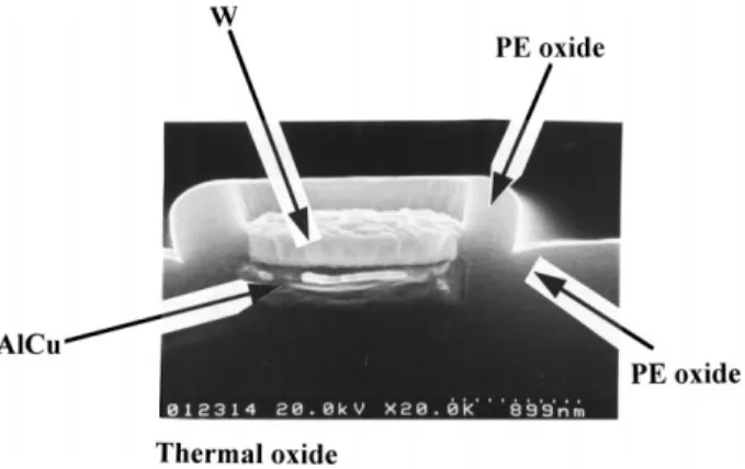
carrier gas ¯ow-rate 1000 sccm, and growth time 150 s. The cross-section images of the W-plugs were obtained with a scanning electron microscope (SEM) as shown in Fig. 1. After the selective tungsten plug deposition, metal II(Ti/TiN/AlCu/TiN) were deposited on the substrate to a thickness of 900 nm. Then, all samples were patterned by RIE to obtain the upper metal strips for the electrode of electrical measurement. The cross-section of the via struc-ture was shown in Fig. 2. Finally, via resistance of AlCu/W/ AlCu structure was measured by the four-terminal Kelvin structure as shown in Fig. 3.
Fig. 1. SEM cross-section images of W deposition in via holes.
3. Results and discussion
Fig. 4 shows the SEM cross-section images of W deposi-tion in Al via holes with various precleanings. In Fig. 4a, there were only a little tungsten islands deposited in the Al via when the Al via was only precleaned by the deionized water (DI water) rinse. It is shown that tungsten can not be easily deposited on the Al via because aluminum oxide on the surface blocks the nucleation of tungsten. With BCl3
plasma etching for 60 s, creep-up and selectivity loss of
CVD-W deposition was observed, as shown in Fig. 4b. The result is thought to be due to outsputtered aluminum oxide and aluminum atoms induced tungsten nucleation on the sidewall of via and the surface of the dielectric layer. However, the selectivity of CVD-W can be signi®cantly improved by cleaning the via in a hydroxylamine sulfate solution, as shown in Fig. 4c.
For the electrical characterization, via resistance of AlCu/ W/AlCu was measured using a four-terminal Kelvin struc-ture. Fig. 5 shows the measured speci®c via resistance of
Fig. 4. SEM cross-section images of W deposition in via holes with the various precleanings. (a) Deionized water rinse, (No W deposition); (b) sample A with 50W BCl3plasma etching,(loss of CVD-W selectivity); (c) sample B with diluted hydroxylamine sulfate wet etching,(good selectivity); (d) sample C was
treated with two-step cleaning (good selectivity); (e) sample D with dipped in mixed solution of 0.1 M hydroxylamine sulfate and 0.1 M CuSO4for 1 min at
samples A±E. Compared with the sample only pre-cleaned by DI water, the speci®c via resistances of sample A and sample B are much lower than that of DI water pre-cleaned sample. The speci®c via resistances for the sample B is slightly higher than that of sample A. It is presumably due to the reoxidation of the aluminum surface during the short period of time when sample B was exposed to the ambient air before loading into the tungsten deposition chamber. To resolve this issue, we developed the new cleaning solution, hydroxylamine sulfate [(NH2OH)2H2SO4] combined with
CuSO4. Hydroxylamine sulfate is capable of dissolving
aluminum oxide (Al2O3) and leave the fresh Al surface on
the bottom of via. A previous paper has demonstrated the clean effect of hydroxylamine sulfate on Al via [8]. Conse-quently, the native aluminum oxide can be completely removed and fresh underlying aluminum would be exposed. The copper ion contributed from CuSO4 will react with
clean aluminum and then form a very thin elemental copper layer on the bottoms of via according to the following reac-tions [9].
Cu211 2e2! Cu E0 0:34 VSHE 1
Al311 3e2! Al E0 21:66 VSHE 2
where E0is the half-cell reduction potential in volts with
respect to the standard hydrogen electrode (VSHE).
Combin-ing Eqs. (1) and (2) to complete the full redox reaction, as follows
3Cu211 2Al ! 3Cu 1 2Al31 D E0 2:0 V 3 where the reaction is expected to be spontaneous owing to its negative free energy. Finally, a DI water rinse is neces-sary for removing the by-products of this redox reaction.
To observe the SEM cross-section images of samples B and C, good selectivity of CVD-W could be obtained. It is shown in Fig. 4c,d. In addition, the speci®c via resistance of sample C is slightly lower than those of samples A and B. It is presumed that little copper ions reacted with partial area of clean aluminum surface to form a very thin elemental copper layer on the parts of bottom of via. So the speci®c via resis-tance of sample C is slightly lower then samples A and B.
The two-step cleaning process is as follows: Step I: the wafers were dipped in 0.1 M diluted solution of hydroxyla-mine sulfate for 1 min at 508C. Step II: the wafers were sequentially dipped in 0.1 M CuSO4solution for 1 min at
608C. It is found that Al2O3could be removed by
hydroxy-lamine sulfate. During the short period of transferring from step I to step II, however, sample C was exposed to the ambient air. Slight reoxidation of the aluminum surface would be still occurred before copper layer passivation. This induces that the via resistance of sample C is not much lower than that of sample B.
Hydroxylamine sulfate mixed with CuSO4could be used
to reduce the chance of fresh aluminum surface exposed to the ambient air. Once Al2O3 was removed by
hydroxyla-mine sulfate, the copper ions would immediately react with clean aluminum and then form a very thin elemental copper layer on the bottoms of via. This copper layer would prevent the fresh aluminum surface from reoxidation.
Fig. 4d,e shows the SEM cross-section images of samples C and D at 508C precleaning temperature. In our experi-ment, it is found that 508C precleaning temperature is the optimum condition. From Fig. 4d,e, the image of W deposi-tion in Al via of sample D is smoother than that of sample C and good selectivity of tungsten plug is obtained also. In addition, the via resistance of sample D is the minimum one, as shown in Fig. 5. The reason is that copper can passivate the clean Al surface as well as copper is more stable and harder to be oxidized than aluminum as exposed in the environment. Therefore, a low via resistance and good selectivity of tungsten plug is obtained when the Al via is precleaned with this new cleaning solution.
4. Conclusions
In this work, the effects of a new precleaning solution were investigated. For conventional precleaning BCl3
-based plasma-etches, it is found that creep-up and selectiv-ity loss resulted from the outsputtered aluminum oxide and/ or aluminum atoms redeposited on the sidewall of via as well as on the surface of the SiO2. However, excellent
selec-tive CVD-W can be obtained by using the hydroxylamine sulfate mixed with CuSO4to clean the Al via holes. This
precleaning solution not only removes the metal oxide at the bottom of aluminum via, but also in-situ forms a very thin copper passivation layer on the Al surface to prevent alumi-num surface reoxidation during the time of loading into the W deposition chamber. A low via resistance and good
selec-Fig. 5. The speci®c via resistances of samples A±D, respectively, as compared with the sample only pre-cleaned by DI water.
tivity of tungsten plug can be obtained as the via is cleaned by this new solution. Thus, signal propagation time delay can be signi®cantly reduced due to the low via resistance. Therefore, high performance in electrical characteristics can be achieved.
Acknowledgements
This work was performed at the National Nano Device Laboratory and was supported by the National Science Council of the Republic of China under Contracts, No. NSC87-2721-2317-200 and No. NSC87-2215-E317-002. References
[1] R.H. Wilison, R.W. Stall, M.A. Calacone, VMIC Proc., , 1985, pp. 343.
[2] D.M. Drown, B. Horowitz, P. Piacente, R. Wilson, D. Woodruff, Elec-tron Device Lett. 8 (1987) 55.
[3] C. Kaanta, W. Cote, J. Cronin, K. Holland, P.I. Lee, T. Wright, IEEM IDEM Proc., , 1987, pp. 218.
[4] J.E.J . Schmitz, Chemical Vapor Deposition of Tungsten and Tungsten Silicide, Noyes Publications, NJ, 1992, pp. 75±80.
[5] V.V.S. Rana, J.A. Taylor, L.H. Holschwandner, N.S. Tsai, in: E.K. Broadent (Ed.), Tungsten and Other Refractory Metals for VLSI Appli-cations II, Materials Research Society, Pittsburgh, PA, 1987, pp. 187.
[6] R.C. Ellwanger, J.E.J. Schmitz, A.J.M. Van Dijk, in: V.A. Wells (Ed.), Tungsten and Other Refractory Metals for VLSI Applications III, Materials Research Society, Pittsburgh, PA, 1988, pp. 399.
[7] E. Nishitani, S. Tsuzuku, in: V.S. Furukawa, S. Wong (Eds.), Tungsten and Other Refractory Metals for ULSI/VLSI Applications, Materials Research Society, Pittsburgh, PA, 1990, pp. 61.
[8] Yeh Wen-Kuuan, Tsai Ming-Hsing, Chen Sheng-Hsiung, Chen Mao-Chieh, Wang Pei-Jan, Liu Lu-Min, Lin Mou-Shiung, J. Electrochem. Soc. 142 (1995) 3584.