國
立
交
通
大
學
電子物理學系
博
士
論
文
氮化銦鎵/氮化鎵量子井聯合能態密度的變化及 V 型
結構對元件特性的影響
Optical joint density of states and effects of V-shaped structures in
InGaN/GaN quantum wells
研 究 生:王俞授
指導教授:陳振芳 博士
氮化銦鎵/氮化鎵量子井聯合能態密度的變化及 V 型結構對元件特
性的影響
Optical joint density of states and effects of V-shaped structures in
InGaN/GaN quantum wells
研 究 生:王俞授 Student:Yu-shou Wang 指導教授:陳振芳 Advisor:Dr. Jenn-Fang Chen
國 立 交 通 大 學 電 子 物 理 學 系
博 士 論 文
A Thesis
Submitted to Department of Electro-physics College of Science
National Chiao Tung University in partial Fulfillment of the Requirements
for the Degree of Master
In Electro-physics
June 2012
Hsinchu, Taiwan, Republic of China
i
致謝
漫長的六年博士生涯期間,經歷過各種嚴峻挑戰,從執行計畫遇到無法突破的瓶頸、 發表論文不斷地被退稿、實驗上不斷出現與預期不符的結果以及實驗機台遇到突發的故 障,然而這些挫折隨著持續不斷的挑戰被一一克服了,並且也順利的完成學位口試,此 時我深刻體會到,這幾年不斷失敗的過程與歷練比贏得博士學位更有價值,我也會不斷 地警惕要時時刻刻保持謙虛學習的態度進入社會。 首先感謝我的指導教授陳振芳老師給予我充分的自由從事研究並適時的給予指導,也 特別感謝我的共同指導教授陳乃權老師,從我大學專題生時就給予我特別的關懷,非常 感激你多年來的苦心栽培與指導,我會銘記在心。 感謝教導我 MOCVD 的施權峰老師以及感謝 MOCVD 實驗室的狗海與大鳥從大學一 路到博士班的陪伴,一起體會研究生的辛酸,一起打籃球相約到台北看晚場的電影,讓 我的求學過程一點都不寂寞,感謝每次都在旁邊笑的學弟俊逸,沒有你的幫忙我無法順 利完成我的論文,感謝阿吉哥的鼓勵與幫忙,感謝脾氣火爆的軍人建茗、球技驚讚的小 葉與竣翔、愛打壘球的鈺翔及正妹學妹莞潔在實驗室的幫忙,替實驗室增添不少樂趣。 感謝畢業的邱安平學長,在工作之餘還時常回來實驗室關心學弟妹的狀況並提供寶貴 的建議,感謝建元學長和傑哥,你們都是一路陪伴我從碩士班到博士班一起努力打拼的 好朋友。感謝渠哥及仁智學長,在執行計畫中給予我寶貴的意見和鼓勵。 感謝交大實驗室的同學江振豪,時常給予我寶貴的資訊和鼓勵,感謝學弟謝孟謙,雖 然你每次講話都酸酸的,但是實際上還是很有義氣地給予我協助,感謝政鴻時常在研究 上的交流,讓我獲益良多,也感謝陪我去日本吃鰻魚飯的家峰和學弟妹亞青、國豪、俊 泓、哲倫、敬恩及家偉在口試期間的幫忙。 另外特別感謝一路從碩士班到博士班陪伴我執行計畫的好夥伴宥楠學長,我們一起熬 夜做實驗,一起討論研究的進度,一起分享生活的喜怒哀樂,甚至畢業後也一直關心我 的求學及找工作的狀況,你真的幫助我太多太多了,你不但是我的好學長也是我最好的ii 朋友,真的由衷的感激。 感謝我的父母與弟弟,有了你們長期在背後默默地支持與陪伴,讓我能夠無憂無慮的 完成學業,謝謝你們。 最後感謝我的女朋友李鈞婷,從我碩士班開始就不離不棄的陪伴我到現在,在求學過 程中的酸甜苦辣我們都一起經歷過,相信將來會成為我們共同美好的回憶。 俞授 謹識於新竹風城交大 民國一百零一年六月
iii
氮化銦鎵/氮化鎵量子井聯合能態密度的變化及 V 型結構對
元件特性的影響
研究生 : 王俞授 指導教授 : 陳振芳 博士 國立交通大學電子物理研究所 摘 要 由於 III-V 族氮化鎵具有較寬的材料能隙,再搭配銦及鋁成份的調變,其能隙可從 0.7eV 到 6.2eV,涵蓋了所有可見光的部分。因此 III-V 族氮化物適合作為發光二極體的 材料,近年來更被廣泛的應用在指示燈、顯示器的背光源及照明上,然而受限其磊晶基 板的選擇,目前較為普遍使用的藍寶石基板與氮化鎵材料存在著極大的晶格不匹配差 異,因此氮化鎵磊晶結構易形成密度高達 108 ~1010cm-2的貫穿式差排。貫穿式差排一般 被認為是非幅射複合中心,會造成元件的發光效率下降,然而實際上氮化鎵藍光二極體 的發光效率並沒有顯著的下降,這些特徵被認為可能來自銦原子群聚現象所產生的影 響,並持續受到矚目。 本研究是利用有機金屬氣相磊晶機台成長氮化鎵發光二極體元件並針對其複合機制 進行討論。我們引入一套自發性幅射光譜模型可用來描述磷化鋁鎵銦及氮化銦鎵發光二 極體之螢光光譜,並可直接透過元件之螢光光譜,得到其量子井之聯合能態密度分佈, 此方法所取得之聯合能態密度分佈與光電流量測所得到的吸收光譜相符。進一步的利用 聯合能態密度分佈分析不同波長之氮化物發光二極體(紫光、藍光、綠光)隨電流變化的 影響,發現波長隨電流增加所產生之藍移現象與聯合能態密度的變化息息相關。該現象 可以解釋為當外加電流時,量子井的極化現象受到額外注入的載子而產生屏蔽效應,進 而產生波長藍移。而低能態之聯合能態密度則是反應出銦原子群聚所形成之局部能態的 現象,並導致較寬的螢光光譜。iv 另外,透過變溫光激螢光及時間解析螢光光譜分析載子在氮化物發光二極體中之動態 行為。研究發現幅射複合的位置主要發生在銦聚集所形成之局部低能態,此局部低能態 可以有效的捕捉載子防止載子擴散至貫穿式差排的位置產生非幅射複合使得發光效率 下降。 最後我們研究 V 型結構於量子井對氮化物發光二極體元件的影響。V 型結構是透過貫 穿式差排所形成,其側邊所形成之較窄的多重量子井結構可提供較大的能隙,防止一般 量子井中的載子與貫穿式差排產生非幅射複合。研究並指出,透過磊晶填平 V 型結構可 形成電流阻擋層,進一步抑制電流的注入貫穿式差排,因此氮化物發光二極體可透過此 磊晶結構的調整大幅的改善其發光效率。
v
Optical joint density of states and effects of V-shaped structures in InGaN/GaN quantum wells
Student : Yu-Shou Wang Advisor : Dr. Jenn-Fang Chen Department of Electrophysics
National Chiao Tung University
Abstract
The wide range of energy gaps in group-III nitride-based materials allows for adjustment of the direct band gap energies from 0.7eV to 6.2eV by varying the compositions of In and Al contents, including all visible energy. Therefore, among the many commercial applications of nitride-based light-emitting diodes (LEDs) include indicator lights, backlight displays and light bulbs. However, these devices typically have a high density of dislocations (108–1010cm-2) that thread through active regions, due to the significant lattice mismatch between nitride epilayers and sapphire substrates. Although being identified as efficient nonradiative centers, threading dislocations do not significantly degrade the performances of LEDs. This feature is recognized as the effects of self-formed In-rich regions in InGaN quantum wells and continues to draw considerable attention, thus warranting further study.
This work studies the recombination mechanism of InGaN LEDs grown by metal organic chemical vapor deposition. An analytical method is also developed for determining the optical joint densities of states of AlGaInP LEDs and InGaN LEDs. Capable of extracting the optical joint density of states, the proposed method can be obtained from photoluminescence (PL) or electroluminescence spectrum of the devices, results of which correlate with the absorption spectrum evaluated by photo current measurements. Furthermore, the optical joint densities of
vi
states of three InGaN LEDs with different emission wavelengths (violet, blue and green) operated at various currents are examined. Experimental results indicate that the blueshift of the emissions with an increasing current is related to the variation in optical joint densities of states and can be attributed to the carrier screening of quantum-confined Stark effect induced by the piezoelectric field. Tails at the low-energy end of the density of states, corresponding to localized states, is found, and these tails broaden the spectra of the devices.
Moreover, the carrier dynamic process of InGaN LEDs is investigated by using temperature dependence of PL and time-resolved PL. Experimental results indicate that the internal high efficiency of InGaN LEDs is mainly related to the spontaneously formed In-rich regions. The electron-hole pairs injected into wells typically drift to low-energy locations and then recombine radiatively rather than diffuse to dislocations.
Furthermore, the extent to which V-shaped structures affect the internal quantum efficiency of nitride LEDs is investigated. The V-shaped structures are initiated at threading dislocations, subsequently enclosing them. Since quantum wells grown on the sidewalls of V-shaped structures are thin, electron and hole transition energy is higher than that of normal wells due to the quantum confinement effect. This increased energy functions as a potential barrier, preventing carriers in normal wells from diffusing into dislocations. Moreover, our sample contains an unintentionally formed current blocking mechanism, suppressing the current density in the region around dislocations. Since both possible paths have been blocked, electrically injected electron-hole pairs cannot generally reach the dislocations, reducing drawbacks associated with threading dislocations in nitride LEDs.
vii
Table of contents
Acknowledgements ... i
Abstract (in Chinese) ... iii
Abstract ... v
Table of contents ... vii
List of figures ... x Chapter 1 Introduction ... 1 Reference ... 4 Chapter 2 Background ... 5 2.1 Epitaxial technique ... 5 2.2 MOCVD ... 5 2.3 Photoluminescence ... 7 2.4 Electroluminescence ... 7
2.5 Scanning electron microscope ... 7
2.6 Transmission electron microscopy ... 8
Reference ... 9
Chapter 3 Spontaneous emission spectrum in light-emitting diodes ... 14
3.1 Introduction ... 14
3.2 Optical joint density of state ... 14
3.3 Spontaneous emission ... 17 3.4 Absorption ... 18 3.5 Emission spectrum ... 19 3.6 Photo current ... 20 3.7 Conclusion ... 22 Reference ... 23
viii
Chapter 4 Optical joint density of states in InGaN/GaN multiple-quantum-well
light-emitting diodes ... 36
4.1 Introduction ... 36
4.2 Current dependent... 38
4.3 Temperature dependent ... 42
Reference ... 45
Chapter 5 Diffusion-controlled effects of luminescence efficiency in InGaN/GaN light-emitting diodes ... 63
5.1 Introduction ... 63
5.2 Experiments ... 64
5.3 Transmission electron microscopy ... 65
5.4 Photoluminescence ... 65 5.5 Time-resolved photoluminescence ... 66 5.6 Radiative lifetime ... 68 5.7 Nonradiative lifetime ... 70 5.8 Conclusion ... 74 References ... 75
Chapter 6 Potential barriers and current-blocking structures induced by V-shaped pits in InGaN/GaN light-emitting diodes ... 88
6.1 Introduction ... 88
6.2 Experiments ... 89
6.3 Transmission electron microscopy ... 89
6.4 Photoluminescence ... 98
6.5 Electroluminescence ... 92
6.6 Conclusions ... 94
ix Publish list ... 111 A. Refereed Papers ... 111 B. Conference papers ... 111 a. International conference ... 111 b. Domestic conference ... 113
x
List of figures
Fig. 2.1 MOCVD Aixtron 200/4 RF-s ... 10
Fig. 2.2 Deposition process ... 10
Fig. 2.3 Reactor of MOCVD ... 11
Fig. 2.4 Sapphire substract and susceptor... 11
Fig. 2.5 RF-Coil and lightpipe ... 12
Fig. 2.6 In-situ reflectometry ... 12
Fig. 2.7 PL measurement ... 13
Fig. 2.8 EL measurement ... 13
Fig. 3.1 Dispersion relation of electron-hole recombination and phonon emission ... 24
Fig. 3.2 Density of states in two-dimensional ... 25
Fig. 3.3 Theoretical emission spectrum in two-dimensional quantum structure ... 25
Fig. 3.4 Theoretical emission spectrum of an LED ... 26
Fig. 3.5 Sample structure of an AlGaInP LED ... 27
Fig. 3.6 Power spectra of the LED measured at 10 mA, and the temperature ranges from 400 to 120 K ... 28
Fig. 3.7 Photon density spectra measured at 10 mA on a semi-log scale and the temperature ranges from 400K to 120K ... 28
Fig. 3.8 Junction temperature obtained from gradients of high-energy tails in an EL spectrum at 300K ... 29
Fig. 3.9 Dependences of junction temperatures on ambient temperatures obtained from gradients of high-energy tails ... 29
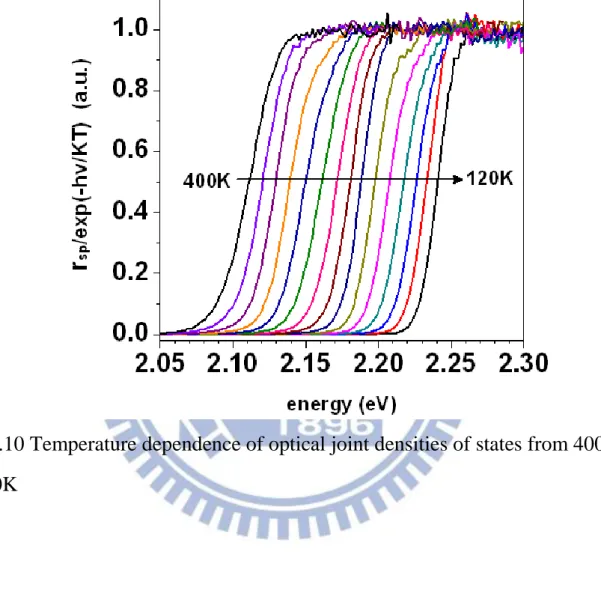
Fig. 3.10 Temperature dependence of optical joint densities of states form 400K to 120K ... 30
xi
Fig. 3.12 Sample structure of the yellow LED ... 31
Fig. 3.13 Sample structure of the yellow-green LED ... 32
Fig. 3.14 Photo current spectrum and EL spectrum of the red LED ... 32
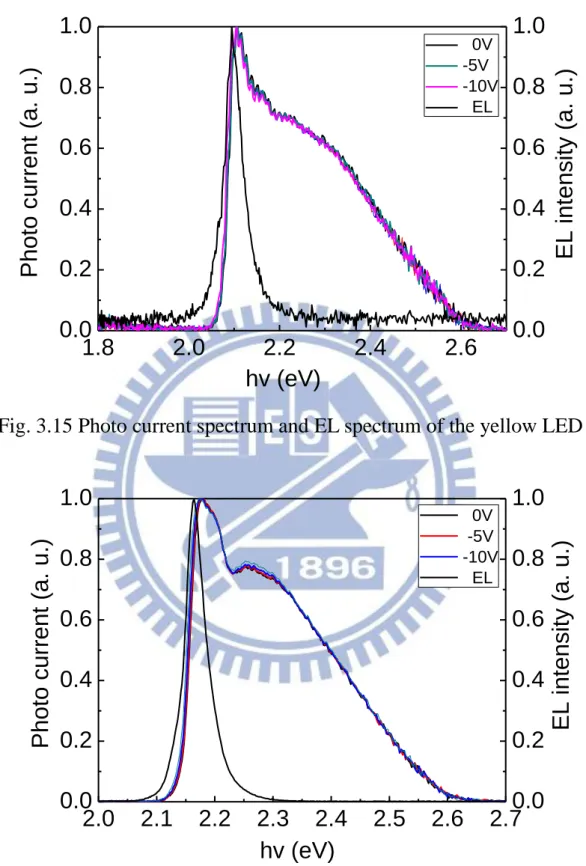
Fig. 3.15 Photo current spectrum and EL spectrum of the yellow LED ... 33
Fig. 3.16 Photo current spectrum and EL spectrum of the yellow-green LED ... 33
Fig. 3.17 Simulation of the DBR ... 34
Fig. 3.18 Absorption spectrum of GaP in red LED ... 34
Fig. 3.19 Absorption spectrum of GaP in yellow LED ... 35
Fig. 3.20 Absorption spectrum of GaP in yellow-green LED ... 35
Fig. 4.1 EL spectra of (a) violet, (b) blue, and (c) green InGaN/GaN-based LEDs at various currents from 10 to 80 mA at 300K. Emission peak shifts in the three spectra are 0 meV, 19 meV, and 37 meV, respectively ... 49
Fig. 4.2 Relative optical joint density of states in violet, blue, and green LEDs under currents from 10 to 80 mA, calculated by dividing EL spectra by thermal distribution ... 50
Fig. 4.3 Band diagrams and wave functions of elections and holes under (a) piezoelectric field and (b) screened piezoelectric field ... 51
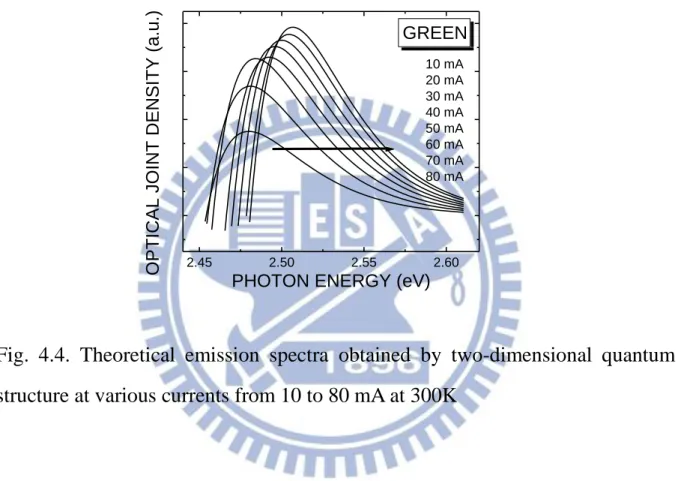
Fig. 4.4 Theoretical emission spectra obtained by two-dimensional quantum structure at various currents from 10 to 80 mA at 300K ... 53
Fig. 4.5 Experimental and theoretical EL peak shifts with current in blue (green) LED are denoted by solid circles (solid squares) and open circles (open squares), respectively ... 54
Fig. 4.6 The FWHMs of the experimental spectra and simulated spectra for violet, blue and green LEDs ... 56
xii
Fig. 4.7 PL spectra of an LED at various temperatures from 20 to 340K ... 57 Fig. 4.8 The emission peak positions of the PL spectra at various temperatures from 20
to 340K ... 57 Fig. 4.9 Relative optical joint density of states under temperatures from 20 to 340K,
calculated by dividing PL spectra by thermal distribution ... 58 Fig. 4.10 The linear fitted lines of the steep increased of optical joint density of states at
140K, 240K and 340K ... 58 Fig. 4.11 The theoretical emission spectra obtained by two-dimensional quantum structure from 20 to 340K ... 59 Fig. 4.12 The optical joint density of states with eliminating linear fitted lines at 140K,
240K and 340K ... 60 Fig. 4.13 The theoretical emission spectra obtained by localized states from 20 to
340K ... 60 Fig. 4.14 The peak positions of experimental emission spectrum and theoretical emission
spectrum obtained by two-dimensional quantum structure and localized states from 60 to 340K ... 61 Fig. 4.15 The experimental emission spectrum and theoretical emission spectrum obtained
by two-dimensional quantum structure and localized states at (a) 140 K and (b) 340K ... 62 Fig. 5.1 Diffusion-controlled kinetics of recombination process for line-sink defects ... 77 Fig. 5.2 Cross-sectional TEM image of the LED structure. Inset: magnified TEM shows
a dislocation thread through the active layers where point A is the location of active layers and point B is the location of a dislocation ... 78 Fig. 5.3 Temperature dependence of PL spectra ... 79 Fig. 5.4 The fitted Arrhenius plot of the PL intensity ... 80 Fig. 5.5 (a) Temperature dependence of TRPL (b)Temperature dependence of the PL
xiii
Fig. 5.6. (a) Arrhenius plot of the PL intensity. (b) The temperature dependence of carrier lifetime, radiative lifetime and nonradiative lifetime, respectively ... 82 Fig. 5.7 Schematic band diagram of the recombination processes with carriers and
dislocations ... 83 Fig. 5.8 (a) PL spectrum at 20K. (b) PL decay time as function of the emission energy .. 84 Fig. 5.9 The Schematic representation of localized excitonic states and processes in
GaAs1-xPx alloys ... 85
Fig. 5.10 The PL spectrum at 20K with PL decay time as function of the emission energy ... 86 Fig. 5.11 Temperature dependence of nonradiative lifeitme. The trend of nonradiative
lifetime with varied temperature is controlled by diffusivity ... 87 Fig. 6.1 Sample structure ... 98 Fig. 6.2 (a) Cross-sectional TEM image of the LED structure. (b) The magnified image
of a V-shaped pit. The well grown on the sidewall is narrower than that on the c-plane ... 99 Fig. 6.3 The Cross-sectional TEM images of the MQWs on normal plane ... 100 Fig. 6.4 (a) These V-shaped pits have a six-wall structure with the walls corresponding
to the six symmetrical {1011} planes. (b) The void associated with V-shaped pits can be filled by p-type layers ... 101 Fig. 6.5 (a) Cross-sectional TEM image of the LED structure. (b) Magnified image of a
V-shaped pit. The dashed line shows one quantum well, and A, B, and C identify three different points in the well ... 102 Fig. 6.6 (a) The PL spectra measured at different temperatures. (b) The log scale of the
PL spectra ... 103 Fig. 6.7 (a) The PL spectra measured at different temperatures. (b) The PL intensities
and intensity ratio of the high-energy peak and main peak in (a) ... 104 Fig. 6.8 Band diagram of the well along the dashed line (Fig. 1(b)). A, B, and C
xiv
denote different points and correspond to A, B, and C in Fig. 1(b), respectively. The solid lines denote the conduction band and valence band edges, while dashed lines denote the ground-states of electrons and holes. The electrons and holes are denoted by solid and empty circles, respectively ... 105 Fig. 6.9 The EL spectra of the device measured under 20mA injection at different
temperatures ... 106 Fig. 6.10 The EL spectra of the device measured under 20mA injection in the different
range of temperatures. (a) 60K - 160K (b) 170K – 300K ... 107 Fig. 6.11 Normalization of the PL and EL spectra at (a) 50K (b) 140K (c) 300K ... 109 Fig. 6.12 (a) The EL spectra of the device measured under 20mA injection at different
temperatures. (b) The EL intensities and intensity ratio of the high-energy peak and main peak in (a) ... 110
1
Chapter 1 Introduction
Gallium nitride (GaN) is a wurtzite crystal structure with wide bandgap, high heat capacity, high breakdown voltage and high thermal conductivity [1]. Therefore, these materials are commonly used in many high power devices, such as detectors, high power amplifiers, high electron mobility transistors (HEMTs), light-emitting diodes (LEDs) and laser diodes (LDs) [2].
GaN of high crystalline quality can be obtained by using low temperature deposited buffer layer technology. This technology successfully led to the commercialization of high performance of nitride based devices. In recently years, nitride LEDs are widely used in many applications due to their special properties, such as outdoor display, backlighting, traffic signals and illumination. The dramatic increase of the development can be mainly attributed to the improvement of the light efficiency of these devices. However, due to the significant lattice mismatch between nitride epilayers and sapphire substrates (around 13%) [3], these devices typically have a high density of dislocations (108–1010cm-2) that thread through active regions. Although threading dislocations have been identified as efficient nonradiative centers, the performances of LEDs are not significantly decreased by these dislocations [4]. Although much investigation of these structures has been reported in decades, the mechanism of emission luminescence is still much left unknown. Therefore, we aimed at the recombination mechanism of the nitride LEDs. In chapter 2, we introduced the experimental procedures of our research. The InGaN/GaN-based LEDs in our work were grown by using metal organic chemical vapor
2
deposition (MOCVD).Following crystal growth, the wafers were processed to form standard LEDs for electrical injection measurements. In chapter 3, a model for describing the shape of the spontaneous emission spectrum from a quantum-well structure [5] was presented. Based on this model, the coexisting carrier thermal broadening and effective band gap broadening in the spontaneous emission spectrum can be separated from each other. In chapter 4, the optical joint densities of states of three InGaN/GaN-based LEDs with different emission wavelengths (violet, blue and green) operated at various currents was investigated. The results indicate that the blueshift of the emission with increasing current is related to the variation in optical joint density of states. Thus, the blueshift is ascribed to the screening of the piezoelectric field by carriers [6]. A tail at the low-energy end of the density of states, corresponding to localized states, was found, and the presence of these tails broadens the spectra of the devices. In chapter 5, the recombination process in InGaN/GaN LEDs by temperature dependence of photoluminescence (PL) and time-resolved photoluminescence (TRPL) was investigated. The decrease of luminescence efficiency with temperature is related to the increase of radiative lifetime and decrease of nonradiative lifetime. Since threading dislocations which recognized as nonradiative center are locally distributed, the diffusion-controlled kinetic should be considered. Our results exhibited that the nonradiative lifetime is mainly attributed to the diffusion-controlled kinetic rather than Shockley-Read-Hall (SRH) theory and in agreement with the theoretical result. In Chapter 6, the influences of V-shaped pits on the internal quantum efficiency of nitride LEDs were investigated. The V-shaped pits are initiated at threading dislocations and, thus, enclose them. Since quantum wells grown on the sidewalls of V-shaped pits are thin, electron and hole transition energy is higher
3
than that of normal wells due to the quantum confinement effect. This increased energy acts as a potential barrier, preventing carriers in normal wells from diffusing into dislocations. Moreover, an unintentionally formed current blocking mechanism exists in our sample, and can suppress the current density in the region around dislocations. Since both possible paths have been blocked, electrically injected electron-hole pairs cannot generally reach the dislocations and, thus, the drawbacks associated with threading dislocations in nitride LEDs are effectively reduced.
4
Reference
[1] J. Karpinski and S. Porowski, J. Cryst. Growth 66(1) 11 (1984)
[2] S. Nakamura and G. Fasol, The blue laser diode, Springer-Verlag, Berlin, pp.277 (1997)
[3] S. Nakamura, T. Mukai, M. Senoh, and N. Iwasa, J. Appl. Phys. 31(2B), L139 (1992)
[4] S. Nakamura, IEICE Trans. E83-C(4), 529 (2000)
[5] N. C. Chen, C. M. Lin, C. Shen, W. C. Lien, and T. Y. Lin, Opt. Express 16, 20759 (2008).
[6] Y. S. Wang, N. C. Chen, C. Y. Lu, and J. F. Chen, , Physica B. 406, 4300 (2011).
5
Chapter 2 Background
2.1 Epitaxial technique
Many epitaxial techniques are available for growth of semiconductor materials, such as liquid-phase epitaxy (LPE), hydride vapor-phase epitaxy (HVPE), molecular-beam epitaxy (MBE), chemical-beam epitaxy (CBE) and metal organic chemical vapor deposition (MOCVD) [1]. In recent years, high quality epitaxial III-V films and heterostructures for devices have been accomplished by MOCVD technique. MOCVD is a nonequilibrium growth technique relies on vapor transport of the precursors and subsequent reactions of group III alkyls and group V hydrides in a heated zone. This technique originated from Manasevit (1968) who demonstrated that triethylgallium (TEGa) and arsine deposited single crystal GaAs pyrolytically in an open tube cold-water reactor. Manasevit (1960) [2-4] and Hess (1979) subsequently expanded the use of this technique for growth of GaAsP, GaAsSb, and Al containing compound. Today, the MOCVD techniques are frequently used for commercial production operations.
2.2 MOCVD
In this study, MOCVD Aixtron 200/4 RF-s was used [5], as shown in Fig. 2.1. It is a system for epitaxial growth of uniform layers of all III-V and nitride semiconductors. It can be used in research and development as well as in production areas. The chemical reaction of GaN is using triethylgallium (TEGa) or trimethylgallium (TMGa) and ammonia (NH3) as source gases for group III
6
by a carrier gas such as hydrogen (H2) or nitrogen (N2). Figure 2.2 shows the
basic reaction GaN and can be briefly described as below:
CH3
3 NH3 GaN 3CH4Ga ... (1.1)
The precursors do not mix until they reach the chamber, as shown in Fig. 2.3, and the chemical reaction of precursors can occur at the surface of the substrate by controlling the temperature of the substrate. The substrates usually rests on a block of graphite called a susceptor (Fig. 2.4) that can be heated by a radio frequency (RF) coil, as shown in Fig. 2.5. The reactor of the MOCVD is a chamber of a material that does not react with chemicals being used. It must withstand high temperatures. This chamber is composed of liner, a susceptor, gas injection units, and temperature control units. The cooling water must be flowing through the channels within the reactor walls to prevent overheating. In chamber, only the susceptor is heated that gases do not react before they reach the wafer surface. To enhance the uniformity of the deposited films, a rotating susceptor was used. The horizontal reactor permits the handling of up to 1 x 4 inch wafers and the pressure of the system can be pumped from 1000 to 10-3 mbar. The wafer size we used is 2 inch. Basically, the reactor is operated under 50~100 mbar. The rotation rate is kept in 100~120 rpm and controlled by gas flow while the epilayers were growth. The MO sources enter the reactor chamber by carrier gases and stream outward across the deposition zone. In the same time, the susceptor is heated and the deposition reactions on the substrate occur. It is heated with an RF-Coil using the reaction of RF-Frequency generated by an RF-Generator and an oscillator. The temperature can be heated to 1150 ℃ and measured by a lightpipe. During growth process, the growth-rate and crystalline quality of the epilayers can be observed directly by the In-situ
7
reflectometry, as shown in Fig. 2.6. It is used to monitor the reflectance between substrate and epilayers [6,7].
2.3 Photoluminescence
Photoluminescence (PL) is a process in which a substance absorbs photons and then re-radiates photons, as shown in Fig. 2.7. In quantum mechanism, this can be described as an excitation to a higher energy state and then a return to a lower energy state accompanied by the emission of a photon. Therefore, PL can be used as a break-less analysis technology which can reveal the band gap and the carrier transportation behaviors of materials. This is an important technique for measuring the purity and crystalline quality of semiconductor such as GaAs, InP and GaN. In this work, the samples were exited by a 325nm HeCd laser. In addition, some variation of PL measurements was used, such as photoluminescence excitation (PLE) and time-resolved photoluminescence (TRPL).
2.4 Electroluminescence
Electroluminescence (EL) is an optical phenomenon and electrical phenomenon in which a material is produced by current injection and usually measured on processed samples, as shown in Fig. 2.8. It is produced when an electric current is passed through a semiconductor and as excited electrons pass over these holes, they are emitted into the free air as particles known as photons. EL is the results of radiative recombination of electrons and holes in a material. 2.5 Scanning electron microscope
Scanning electron microscope (SEM) is images a sample by scanning it with a high-energy beam of electrons. SEM is one of the widely used tools of modern science for studying morphology and composition of biological and physical materials. It is used to measure the surface properties such as surface topography,
8
composition and electrical conductivity. Moreover, the images of the measurement can magnify up to 100,000x without the need for extensive sample preparation and without damaging the sample. In this work, the JSM-7000F SEM was used.
2.6 Transmission electron microscopy
Transmission electron microscopy (TEM) is a microscopy technique that uses electron beams instead of light to transmit through a very thin film and images the resolution of the thin film allowing for magnification of up to 100,000x and nanometer range. This technique was developed in the 1930s when scientists observed that electrons can be used instead of light to "magnify" objects or specimens under study.
9
Reference
[1] G. B. Stringfellow. Reports on progress in Physics 45 469 (1982) [2] H. M. Manasevit, Appl. Phys. Lett. 116 1725 (1969)
[3] H. M. Manasevit and W. I. Simpson. J. Electrochem. Soc. 12 156 (1968) [4] H. M. Manasevit. J. rys. Growth 13/14 306 (1972)
[5] R. A. Talalaev, E. V. Yakovlev, S. Yu. Karpov, Yu. N. Makarov, O. Schoen, M. Heuken, G. Strauch and Holger Juergensen, MRS Internet J. Nitride Semicond. Res. 4, 5 (1999)
[6] C. Kirchner, and M. Seyboth, Dept. of Optoelectronics, University of Ulm, Annual Report 18 (1999)
[7] K. Christiansen, M. Luenenbuerger, B. Schineller, M. Heuken, and H. Juergensen, Opto-electro. Rev 10(4) 237 (2002)
10
Fig. 2.1 MOCVD Aixtron 200/4 RF-s
11
Fig. 2.3 Reactor of MOCVD
12
Fig. 2.5 RF-Coil and lightpipe
13
Fig. 2.7 PL measurement
14
Chapter3 Spontaneous emission spectrum in light-emitting
diodes
3.1 Introduction
This work presents a model for describing the shape of the spontaneous emission spectrum from a quantum-well structure [1]. A function is introduced to specify the probability distribution for the effective band gap. Based on this model, the coexisting carrier thermal broadening and effective band gap broadening in the spontaneous emission spectrum can be separated from each other. Applying this model to the spectra of AlGaInP light-emitting diodes (LEDs) reveals that the probability distribution functions are almost obtained by Gaussian function. Therefore, the emission spectra can be described by an analytical expression with fitted parameters. Possible reasons for this band gap broadening are discussed. The determination of the junction temperatures from the emission spectra and possible deviations of the results thus determined are also elaborated.
3.2 Optical joint density of state
To fully understand the spontaneous emission spectrum, the definition of optical joint density of state is described. The optical joint density of state is the density of allowable transition states that satisfy the k-selection rule, or equivalently, the density of states for electron-hole pairs. Thus, the definition of density of states in quantum well should be discussed. First, the density of allowed quantum states for a free electron as a function of energy in three-dimensional can be written as:
15 E h m E g 3 2 3 ) 2 ( 4 ) ( ... (3.1)
and the density of energy states in the conduction band and valence can be written as c n c E E h m E g 3 2 3 * ) 2 ( 4 ) ( ... (3.2) E E h m E gv 3p v 2 3 * ) 2 ( 4 ) ( ... (3.3)
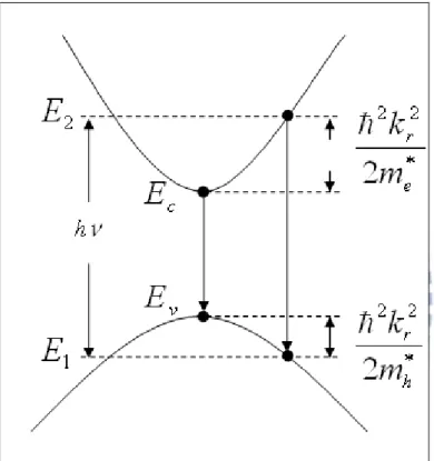
To further consider the density of allowed states for electron-hole pair, an electron-hole recombination process is discussed. Figure 3.1 shows the dispersion relation of electrons in conduction band and holes in valence band. Thus, the photon energy can be written as the joint dispersion relation:
h r e r v c m k m k E E h 2 2 ) ( 2 2 2 2 ... (3.4) where m is the reduced mass given by r
h e r m m m 1 1 1 ... (3.5) To further differentiate Eq. 3.4, we have
h e r h r r e r r r r dE dE dk m k dk m k dk m k dh 2 2 2 r e r e dk m k dE 2 , r h r h dk m k dE 2
and hence we have
2 2 2 2 2 2 2 ) 2 ( 2 2 2 g r r e r r r e r e r e h E m m m m m k m m m k E
16 ( g) e r e h E m m E given by Eq. 3.2 ) ( 2 ) 2 ( ) ( 2 3 2 3 g h e r e e E E m m m E g ... (3.6) using the joint dispersion relation
h dh dE E g( e) e ( ) ... (3.7) where e r e m m dh dE the optical joint density of states in three-dimensional can be written as
g r e r g e r e m h E m m E h m m m h 2 32 3 3 2 2 3 2 ) 2 ( ) ( 2 ) 2 ( ) ( g r E h m h 2 32 3 2 ) 2 ( ) ( ... (3.8) In two-dimensional system, the density of states is a step function, as shown in Fig. 3.2, and the optical joint density of states can be calculated
) ( ) ( 2 u E L m E g ... (3.9) where u()is a step function and Lis the well width
using ( g) e r e h E m m E into Eq 3.9, we have ) ( ) ( 2 * g e e u h E d m E g
... (3.10)Therefore, the optical joint density of states in two-dimensional can be written as
17 e r g e e e m m E h u d m dh dE E g h ) ( ) ( ) ( 2 * ( ) 2r u(h Eg) d m h ... (3.11) wherem is the reduced mass of an electron-hole pair and r u(h Eg)is a step-function.
3.3 Spontaneous emission
For a direct band gap semiconductor, the spontaneous emission rate can be written as [2]: ) ( ) ( 1 ) ( h h fe h r sp ... (3.12)
where ris the radiative lifetime of electron-hole recombination, (h) is the optical joint density of state, fe(h) is the occupancy probability of
electron-hole pairs [3]. Since the occupancy probability of electrons f (E2) in conduction band and the occupancy probability of holes [1 f(E1)] in valance band are both obtained by the Boltzmann distribution, as shown in Fig. 3.3, the occupancy probability of electron-hole pairs can be written as
)] ( 1 )[ ( ) (h f E2 f E1 fe
... (3.13) ) 1 )( 1 ( ] ) 1 ( 1 [ ) 1 ( ) ( 1 2 1 1 2 1 1 KT E E KT E E KT E E KT E E KT E E e fn fp fp fp fn e e e e e h f In low level injection, the occupancy probability of electron-hole pairs can be approximated to [4,5]: KT E E KT E E e fp fn e e E f E f h f 1 2 ] ( 1 )[ ( ) ( 2 1
18 KT E E KT E E e e fp fn 2 1 ... (3.14)
whereEfn Efpis the separation between the quasi-Fermi energies of the electron and the hole. SinceE2 E1 h , the Eq 3.14 can be rewritten as
KT h KT E E e h e e f fp fn ) ( ... (3.15) Therefore, we have the spontaneous emission rate in low level injection
KT h KT E E r sp h h e e fp fn 1 ( ) ) ( ... (3.16)
Using the optical joint density of states in three-dimensional (Eq. 3.8) and two-dimensional (Eq. 3.11), the spontaneous emission rate can be rewritten as
KT h KT E E r g r sp e e E h m h fp fn
2 3 2 3 2 ) 2 ( ) ( (3-D) ... (3.17) KT h KT E E r g r sp e e d E h u m h fp fn ( 2 ) ) ( (2-D) ... (3.18)Therefore, the spontaneous emission spectrum of LEDs can be fully ascribed by the multiplying of optical joint density of states and Boltzmann distribution, as shown in Fig. 3.4.
3.4 Absorption
For a direct band gap semiconductor, the absorption coefficient can be written as: )] ( ) ( )[ ( 8 ) ( 2 h h fa h fe h r )} ( )] ( 1 [ )] ( 1 )[ ( ){ ( 8 2 h f h f h f h f h c v c v r ) ( 8 )] ( ) ( )[ ( 8 2 2 h h f h f h r v c r ……….. (3.19)
19
Since optical joint density of states is a factor of absorption coefficient, the optical joint density of states of LEDs can be obtained from absorption spectrum.
3.5 Emission spectrum
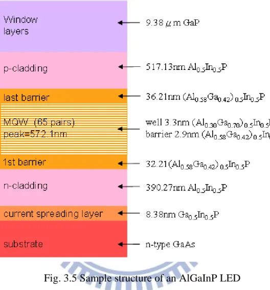
To verify the theoretical theory, an AlGaInP LED with varying temperature (120K to 400K) measured at 10mA was discussed. Figure 3.5 shows the wafer structure of the sample which has an n-type GaAs substrate, a 390-nm-thick
n-type Al0.5In0.5P hole-blocking layer, 65 pairs of multiple quantum wells
(MQWs), each of which comprises a 3.3 nm (Al0.3Ga0.7)0.5In0.5P well / 2.9 nm
(Al0.58Ga0.42)0.5In0.5P barrier, a 517-nm-thick p-type Al0.5In0.5P electron-blocking
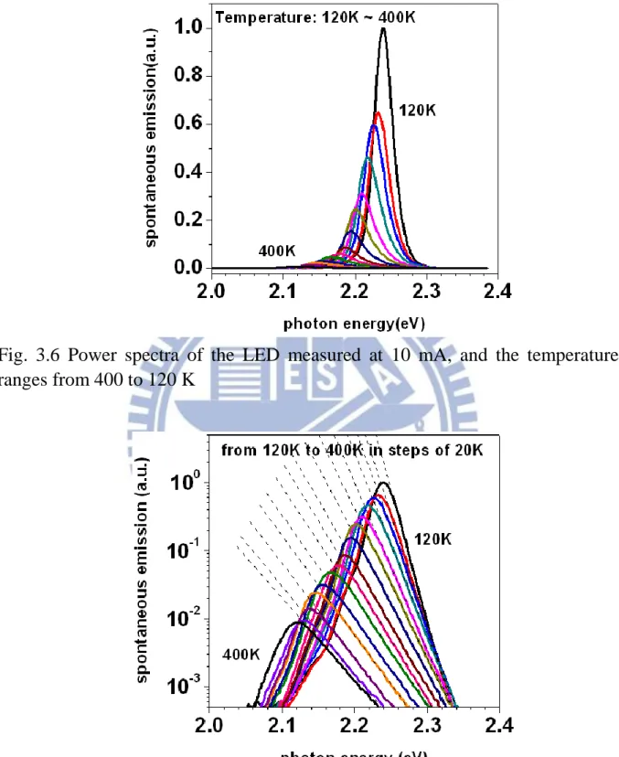
layer, and a 9.38-μm-thick p-type GaP current spreading layer. The sample made from the wafer had an area of 225×225 μm2 and a height of 180 μm. The sample was mounted onto a heat sink using a metal solder. The heat sink was a Bergquist thermal clad substrate with an area of 3×3 cm2 and a height of 0.2 cm. The device spectra were obtained by placing the device onto the sample holder of a cryostat, electrically driving the device, collecting the top emission using a microscope, and then analyzing the wavelength-dependent energy spectral density functions P(λ) using a monochromator and a silicon photodetector. The overall system wavelength-dependent response comprised of the responsivity of the silicon photodetector and the reflectivity of the grating was taken into account. Figure 3.6 presents the spectra of the sample that was operated at 10 mA, at temperatures from 120 to 400 K in steps of 20 K. As the ambient temperature increased, the peaks were redshifted and the intensities attenuated. As each photon represents a transition event in the active layer, the photon density spectrum is more useful than the power spectrum in obtaining information about spontaneous emission and the related phenomena. P(λ) was
20
then transformed to the corresponding frequency-dependent energy spectra
P(hv), according to P(hv)=(λ2/hC0)P(λ), where C0 is the speed of light in a
vacuum and h is Planck’s constant [6].
The relative photon density spectra r(hv) were then obtained using r(hv)=
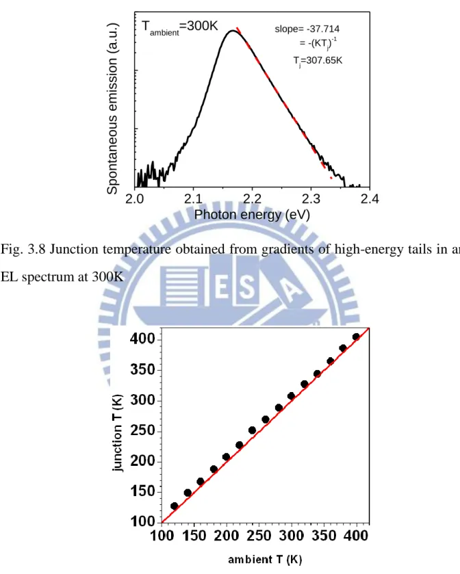
P(hv)/hv, and the results are plotted as solid curves on a semi-log scale in Figs. 3.7. As indicated by the solid curves in Figs. 4, although the ambient temperature covers a rather wide range (from 120 to 400 K), the slopes of the low-energy tails of the measured spectra do not change appreciably with the temperature. This fact is consistent with Eq. 3.16, which states that the low-energy tails of these spectra depend strongly on the broadening of the band gap but weakly on the junction temperature. In contrast, the high-energy tails of these spectra are accurately described by straight lines whose gradients depend strongly on the temperature. Thus, the junction temperatures can be obtained from the high-energy tails of the spectra. Figure 3.8 shows the EL spectrum of the sample at 300K and the dashed line revealed that the junction temperature is around 307.65K, which is very close to the ambient temperature. Figure 3.9 plots the junction temperatures obtained from the gradients, which are very close to the ambient temperatures. This result agrees with the theoretical theory and this method can be applied to measure the junction temperatures from emission spectra. Furthermore, it was also observed that the optical joint densities of states of the sample shift toward higher energy with decreased of temperature, as shown in Fig. 3.10. This result indicated that the shift of the emission spectrum was obtained by the Varshni equation.
3.6 Photo current
Furthermore, the photo-current measurement was used to investigate the absorption spectra of LEDs. Three AlGaInP LEDs with different wavelength
21
(red, yellow and yellow-green) were used. The wafer structure of the samples which has an n-type GaAs substrate, a 600-nm-thick n-type Al0.5In0.5P
hole-blocking layer, a 600-nm-thick p-type Al0.5In0.5P electron-blocking layer,
and a 11μm-thick p-type GaP current spreading layer. The emission wavelength and distributed Bragg reflector (DBR) for each sample was to adjust the structure of MQWs, as shown in Fig. 3.11, Fig. 3.12 and Fig. 313.
Figure 3.14 to figure 3.16 shows the photo-current spectrum under varying reverse bias (0V, -5V, -10V) and EL spectrum measured at 20mA. The photo current spectrum shows independent with reverse bias. It is indicated that the MQWs of the samples are in the depletion regions, thus, when laser excited the electron-hole pairs in MQWs, both electrons and holes will sweep out toward
n-type layer and p-type layer, respectively. At low energy tail, the photo current
spectrum shows similar feature with the EL spectrum. That is due to the optical joint density of state is a factor of the absorption spectrum and emission spectrum (Eq. 3.12 and Eq. 3.19). On the other hand, the increased of the photo current spectrum with interference can be attributed the existence of the DBR under n-type layer. Therefore, the penetrated laser form MQWs can be reflexed to MQWs and reabsorbed. The intensity of the reflection and the width can be simulated from the index of the sample structures, as shown in Fig. 3.17. Moreover, both of the intensity of the photo current spectra decreased when Eg>2.3eV. The reason of the decrease of the intensity can be explained by the
absorption of the GaP. As we assumed that the absorption spectrum of the MQWs is a step function, the absorption spectrum of GaP can be obtained from the dividing the step function and photo current spectrum, as shown in Fig. 3.18, Fig. 3.19 and Fig. 3.20. Despite the influence of the DBR and absorption of GaP, the photo current spectrum shows the same feature with the optical joint density
22
of states obtained from the EL spectrum. This result indicated that the 3.7 Conclusion
This work presents a model for describing the spectra of quantum wells. The carrier temperature can be determined from the high-energy tail of the spectrum and the probability distribution function can be deduced by further numerical processing. This model was applied to an AlGaInP LED, and the measured carrier temperatures were found to be very close to the temperatures. This finding is important evidence of the validity of the proposed model. Two methods are used to obtain the optical joint density of states of the samples. The optical joint density of states can be obtained by dividing the emission spectrum by the Boltzmann distribution function or measured by the photo current measurement.
23
Reference
[1] N. C. Chen, C. M. Lin, C. Shen, W. C. Lien, and T. Y. Lin, Opt. Express 16, 20759 (2008).
[2] B. E. A. Saleh, and M. C. Teich, Fundamentals of Photonics, (John Wiley & Sons, 1991). P.593
[3] H. D. Summers, J. D. Thomson, P. M. Smowton, P. Blood, and M. Hopkinson, Semicon. Sci. Tech., vol.16, p.140, (2001).
[4] P. Blood, E. D. Fletcher, P. J. Hulyer, and P. M. Smowton, Appl. Phys. Lett., vol.48, p.1111, (1986).
[5] P. Blood, A. I. Kucharska, J. P. Jacobs, and K. Griffiths, J. Appl. Phys., vol.70, p.1144, (1991).
[6] N. C. Chen, Y. N. Wang, C. Y. Tseng, and Y. K. Yang, Appl. Phys. Lett. 89, 101114 (2006).
[7] N. C. Chen, W. C. Lien, Y. K. Yang, C. Shen, Y. S. Wang, and J. F. Chen, J. Appl. Phys. 106, 074514 (2009).
24
25
Fig. 3.2 Density of states in two-dimensional
26 (Eg-Eg0 )/Eg -4 -2 0 2 4 P(E g ) (hv-Eg0 )/Eg -4 -2 0 2 4 0.0 0.2 0.4 0.6 0.8 1.0 Eg
27
28
Fig. 3.6 Power spectra of the LED measured at 10 mA, and the temperature ranges from 400 to 120 K
Fig. 3.7 Photon density spectra measured at 10 mA on a semi-log scale and the temperature ranges from 400K to 120K
29 2.0 2.1 2.2 2.3 2.4 slope= -37.714 = -(KT j) -1 Tj=307.65K Spo ntan eo us emi ssio n (a.u.)
Photon energy (eV) Tambient=300K
Fig. 3.8 Junction temperature obtained from gradients of high-energy tails in an EL spectrum at 300K
Fig. 3.9 Dependences of junction temperatures on ambient temperatures obtained from gradients of high-energy tails
30
Fig. 3.10 Temperature dependence of optical joint densities of states from 400K to 120K
31
Fig. 3.11 Sample structure of the red LED
32
Fig. 3.13 Sample structure of the yellow-green LED
1.9 2.0 2.1 2.2 2.3 2.4 2.5 2.6 0.0 0.2 0.4 0.6 0.8 1.0 0.0 0.2 0.4 0.6 0.8 1.0 Photo cu rr en t (a .u.) EL i nten s it y (a.u.) hv (eV) 0V -5V -10V EL
33
1.8
2.0
2.2
2.4
2.6
0.0
0.2
0.4
0.6
0.8
1.0
0.0
0.2
0.4
0.6
0.8
1.0
EL i
nten
s
it
y
(a.
u.)
Photo cu
rr
en
t
(a
.
u.)
hv (eV)
0V -5V -10V ELFig. 3.15 Photo current spectrum and EL spectrum of the yellow LED
2.0
2.1
2.2
2.3
2.4
2.5
2.6
2.7
0.0
0.2
0.4
0.6
0.8
1.0
0.0
0.2
0.4
0.6
0.8
1.0
EL i
nten
s
it
y
(a.
u.)
Photo cu
rr
en
t
(a
.
u.)
hv (eV)
0V -5V -10V EL34 1.8 2.0 2.2 2.4 2.6 0 20 40 60 80 100 Re flectivi ty (%) hv (eV) RED YELLOW YG
Fig. 3.17 Simulation of the DBR
1.8 2.0 2.2 2.4 2.6 2.8 0.0 0.2 0.4 0.6 0.8 1.0 ab sorp tion (a. u.) (cm -1 ) Energy (eV) 0 1000 2000 3000 4000 5000 6000
35 1.8 1.9 2.0 2.1 2.2 2.3 2.4 2.5 2.6 2.7 2.8 (cm -1 ) ab sorp tion (a. u.) Energy (eV) 0 1000 2000 3000 4000 5000 6000
Fig. 3.19 Absorption spectrum of GaP in yellow LED
1.8 2.0 2.2 2.4 2.6 2.8
absorpti
on
(a.u.
)
(
cm
-1)
Energy (eV)
0 1000 2000 3000 4000 5000 6000 7000 800036
Chapter 4 Optical joint density of states in InGaN/GaN
multiple-quantum-well light-emitting diodes
4.1. Introduction
Because of the wide range of energy gaps in group-III nitride-based materials, InGaN/GaN-based multiple quantum wells (MQWs) have been used in a broad range of emission wavelengths, such as blue, green and yellow light-emitting diodes (LEDs) [1]. Although the number of applications of these devices has increased in the past decade, their special features still attract considerable attention. For example, despite their high dislocation density (typically in the range 108-1010 cm-2), their luminescence efficiency is peculiarly higher than expected [2]. Also, a large Stokes-like shift occurs between the emission peak and the absorption edge, and this shift correlates with indium content [3]. Many studies have confirmed that indium atoms are important to these phenomena [4]. Since localized states that result from self-organized In-rich regions are regarded as quantum dots [5] or quantum disks [6], electron-hole pairs are likely associated with the localized states rather than being transferred to threading dislocations that act as nonradiative centers [7,8]. Additionally, the quantum-confined Stark effect (QCSE) that is caused by the piezoelectric field has been found to have a large influence on the emission [9]. Because of a large lattice mismatch between GaN and InGaN, a strong strain-induced piezoelectric field tends to shift the quantum-confined level to lower energy [10]. However, the reasons for the blueshift of the emission peak with increasing current and the anomalous broadening of the full width at half
37
maximum (FWHM) are still under debate. Since both the photoluminescence (PL) and the electroluminescence (EL) peaks are at the absorption tail, some researchers have suggested that the blueshift results mainly from the band filling effect of the localized states that correspond to the formed In-rich regions [11]. Others have argued that the blueshift is related to the screening of the piezoelectric field by carriers [12]. Chichibu et al. [13] argued that the blueshift is a combined effect of band filling of localized states and screening of the QCSE. Notably, most related studies have used PL excitation (PLE) to obtain the absorption spectrum. However, the electrically injected carriers and the corresponding emission prevent the absorption spectrum from being obtained under large forward bias. Therefore, the band filling effect of localized states and the piezoelectric effect with a forward current are difficult to determine, and definitive explanations of the blueshift and anomalous increase in the FWHM are still unavailable. On the other hand, the reason of S-shift (redshift-blueshift-redshift) in InGaN/GaN LEDs with varying temperatures is also need more evidence. The explanation of the S-shift has been study for many decades [14,15]. The recombination mechanism of the InGaN LEDs in different temperature ranges can be explained as follows: (i) For T<50K, since radiative lifetime at the lowest temperature is fast and dominant the recombination process, carriers should recombination radiatively in quantum states before relax down into localized states. Thus, when temperature further increased, carriers relax into localized states and induce emission peak decreased. (ii) For 50K<T<150K, since carriers are recombined in localized states and the occupation of probability in each state by an electron-hole pair should obtained by Boltzmann distribution function. Thus, when temperature increased, the occupation of probability at higher states should increase and induce emission
38
peak increased. (iii) For T>150K, since temperature induced band gap shrinkage dominate the emission peak, the emission peak decrease with increasing temperature [16-19]. However, the research of these current and temperature induced peak shift has left many questions unanswered, more work must be done.
This work presents a method for determining the optical joint density of states of nitride-based LEDs using an EL spectrum instead of a PLE. The proposed method of extracting the optical joint density of states is to divide the EL spectrum by the Boltzmann distribution function, to determine the effect of current on the blueshift and the increase in the FWHM [20]. Similar methods, in the form of relations among spontaneous emission, absorption and gain spectra, have been extensively used in studying the details of InGaAsP, AlGaAs, InGaAs and GaAs laser diodes in various aspects [21-28]. Besides, the authors have successfully explained the carrier dynamics, the redshift of the edge emission, the junction temperature and the broadening of the emission spectrum of AlGaInP LEDs by using this method [29,30]. All of these successful precedents justify the method used in this paper. The samples investigated herein are commercial products that were grown on c-plane sapphire substrates by metal organic vapor deposition. Three InGaN/GaN-based light-emitting diodes with different emission wavelengths (violet, blue and green) were adopted. To obtain their spectra, the devices were placed on a heat sink and operated in pulsed mode with a frequency of 1000Hz and a duty cycle of 10% to diminish any possible effect of Joule heating. Thus, the junction temperatures of the measured devices were determined only by the environment, and the corresponding Boltzmann distribution functions are obtained from the ambient temperatures. 4.2 Current dependent of emission spectra
39
Figure 4.1 presents the normalized EL spectra of the samples under various currents at 300K. The peaks shifted to higher energy as the current increased, and the degree of shift was correlated with the indium content. From 10mA to 80mA, the blueshifts for the violet, blue and green LEDs were 0meV, 19meV and 37meV, respectively. The FWHM for the violet, blue and green LEDs were 89meV, 140meV and 160meV, respectively, indicating that the FWHM was strongly correlated with the indium content but weakly correlated with current density. Similar results concerning the blueshift and the increase in the FWHM have been observed in many studies, including those mentioned above.
To determine how localized states and piezoelectric field affect the spectrum under various currents, the optical joint densities of states of these devices are determined under various currents from the measured spectra. The spontaneous emission spectrum of an LED is [20,29,30]
h
h e h KTr ... (4.1) where h is the optical joint density of states, which is the density of
allowable transition states that satisfy the k-selection rule, or equivalently, the density of states for electron-hole pairs, and ehKT is the Boltzmann distribution function, which describes the probability of occupation of each state by an electron-hole pair. Generally, the optical joint density of states has the same mathematical form as the electron (hole) density of states, except in that the effective mass of electron (hole) should be replaced by the reduced mass of electron-hole pairs [20]. Thus, when the optical joint density of states is obtained, the characteristics of the electron and hole densities of states are also obtained, and the optical joint density of states can easily be deduced from the spontaneous emission spectrum by merely dividing the emission spectrum by
40
the Boltzmann distribution function. Notably, such a method is preferable to PLE, since PLE obtains the optical joint density of states via an absorption spectrum, which cannot be obtained at large forward bias. Figure 4.2 shows the relative optical joint densities of states obtained from the EL spectra. All of these curves show two distinct regions – a low-energy tail and a high-energy region, where the density of states increases steeply with increasing energy. Since the low-energy tails of all of these samples are independent of current, the tails are attributed to the formation of localized states. In contrast, the steep increase of the density of states in the high-energy region indicates that these states correspond to the unlocalized states of the two-dimensional quantum structure [25], and its characteristics depend strongly on the samples. The violet LED yields the largest slope among these samples, and its density is independent of current; for blue and green LEDs, the curves of densities strongly depend on current, and their slopes increase with the current, as revealed by the linear fitted dashed lines. These dependences of density on both the sample and the current can be explained by the effect of the piezoelectric field and the screening of this field by carriers. The large amount of indium in the wells in blue and green LEDs makes the piezoelectric field therein wells significant. This field tilts the potential of the quantum well, as shown in Fig. 4.3(a), and electrons and holes in the same well should be spatially separated on opposite sides of the well. Thus, both the electron-hole wave-function overlap and the effective band gap of the well are decreased [32]. As the operating current was increased, the number of carriers in the wells increased, and the piezoelectric field drove the carriers to screen the field itself. Therefore, both the wave-function overlap and the band gap energy increased, as shown in Fig. 4.3(b). S. F. Chichibu et al. [33] and C. K. Choi et al. [34] reported similar results. Their results reveal that the slope of the
41
absorption edge is determined by the piezoelectric field and can be screened by increasing the Si-doping concentrations in the barriers.
Since the slopes of the densities of states in the high-energy region depend on current, the blueshift of the spectra may be attributed to this phenomenon. To examine quantitatively this possibility, the densities of states of blue and green LEDs at various currents were approximated by the linear fitted dashed lines plotted in Fig. 4.2; then, the theoretical emission spectra were obtained by multiplying these fitted curves by the Boltzmann distribution function, as shown in Fig. 4.4. Figure 4.5 presents the blueshifts that were obtained from these theoretical spectra and from the experiment. The agreement between these two sets of data clearly demonstrates the proposed cause of the blueshift, and provides evidence of the screening of the piezoelectric field by carriers. However, the FWHMs of the simulated spectra are lower than those obtained experimentally, as shown in Fig. 4.6. This discrepancy results from the linear approximations of the densities of states that wholly ignored the existence of localized states in the low-energy tails [5]. Although these localized states are known to be independent of current, as mentioned above, they still contribute appreciably to the emission spectra. In fact, the low-energy sides of the EL spectra are determined by the energy distribution of these localized states. Thus, as the indium content is increased, the low-energy tail should be further extended, and the corresponding FWHM of the emission spectrum should increase.
In summary, the optical joint densities of states of three InGaN/GaN-based LEDs with different emission wavelengths were determined at various currents. The optical joint density of states has two distinct regions, a high-energy region, which corresponds to the unlocalized quantum well states and a low-energy tail,
42
which corresponds to the localized states. As the operating current is increased, the slope of the density of states at high-energy region increases with the screening of the piezoelectric field. This fact causes the peak of the EL spectrum to blue-shift with increasing current. The low-energy tail of the optical joint density of states determines the extension of the low-energy side of the EL spectrum, and this fact explains the anomalous increase in the FWHM of the emission of nitride-based LEDs. Furthermore, both of these effects are enhanced by increasing indium content, which relationship is responsible for the increase in blueshift and FWHM with the emission wavelength of the device.
4.3 Temperature dependent of emission spectra
Figure 4.7 presents the normalized PL spectrum of the sample with varying temperatures from 20K to 340K. Figure 4.8 shows the S-shaped variation with temperature. The peak energy shifts from 2.76eV to 2.75eV when temperature increased from 20K to 80K, and shifts to 2.76eV when temperature increased to 200K. The peak energy shifts to 2.744eV when temperature further increased to 340K.
To further understand the S-shaped shift of the emission peak under various temperatures, the optical joint densities of states of the sample are determined under various temperatures from the measured spectra. Figure 4.9 shows the relative optical joint densities of states obtained from the PL spectra with varying temperature. Similar to the optical joint densities of states obtained from the EL spectra, these curves also show two distinct regions – a low-energy tail and a high-energy region. According to the previous result, the low-energy tails are attributed to the formation of localized states and the steep increase of the density of states in the high-energy regions are attributed to the unlocalized states of the two-dimensional quantum structure. Here, the unlocalized states of the two-dimensional quantum structure can be linear fitted as shown in Fig. 4.10.
43
To further consider the effects of the emission peak by these two regions, the theoretical emission spectra of these two regions were obtained. The theoretical emission spectra of the two-dimensional quantum structure were obtained by using the fitted dish lines multiplying the Boltzmann distribution function, as shown in Fig. 4.11. On the other hand, the optical joint densities of states of localized states can be obtained by divided from the origin optical joint densities of states and linear fitted lines as shown in Fig. 4.12. The theoretical emission spectra of localized states were obtained by multiplying the Boltzmann distribution function, as shown in Fig. 4.13.
To further compare these two theoretical emission spectra with varying temperatures, the theoretical emission peak of the localized states shows S-shaped shift, however, the theoretical emission peak of the two-dimensional quantum structure shows only redshifts, as shown in Fig. 4.14. This result indicates that the S-shaped shift is mainly attributed to the localized states and can be explained by the delocalization of excitons out of potential minima. The emission spectrum corresponded to the quantum structure is only affected by the Varshni redshift of the band gap energy. Furthermore, when the temperature increased to 200K, the emission peak positions are contributed by both localized states and quantum structure and redshifts with temperature. The value of the shifts is smaller than the theoretical emission peak of the localized states, which indicated that the emission spectrum corresponded to the unlocalizated two-dimensional quantum structures become to dominate the PL emission peak.
In summary, the optical joint densities of states of a nitride-based LED were determined with varying temperatures. The optical joint density of states can be divided into two regions, a low-energy tail is attributed to the localized states and a high-energy tail is attributed to the unlocalized states of the two-dimensional quantum well. The theoretical emission spectra of the two regions were obtained by multiplying the Boltzmann distribution function separately. Since the Boltzmann distribution can not be used in the lowest range