國
立
交
通
大
學
電子工程學系 電子研究所
碩
士
論
文
磁性 FePt 奈米點 MIS 電容的異值崩潰電壓的
特性與分析
The Characteristics of Anomalous Breakdown
Strength in Magnetic FePt Nanodots MIS Capacitor
研 究 生:江培維
指導教授:張俊彥 院士
磁性 FePt 奈米點 MIS 電容的異值崩潰電壓的
特性與分析
The Characteristics of Anomalous Breakdown Strength in
Magnetic FePt Nanodots MIS Capacitor
研 究 生:江培維 Student:Pei-Wei Chiang
指導教授:張俊彥 院士 Advisor:Prof. Chun-Yen Chang
國 立 交 通 大 學
電子工程學系 電子研究所
碩 士 論 文
A Thesis
Submitted to Department of Electronics Engineering & Institute of Electronics
College of Electrical and Computer Engineering
National Chiao Tung University
In Partial Fulfillment of the Requirements
For the Degree of
Master
In
Electronics Engineering July 2010
Hsinchu, Taiwan, Republic of China
磁性 FePt 奈米點 MIS 電容的異值崩潰電壓的
特性與分析
學生:江培維 指導教授:張俊彥 院士
國立交通大學電子工程學系電子研究所碩士班
摘要
在半導體的領域中,研究的主流往往是矽半導體、高介電材料、三五族復合 物。多數被視為前段製程汙染物的磁性材料在半導體界上的應用則顯得特別的 少,然而,我們發現磁性物質應用在金-氧-半電容中卻有增強電場電度的特殊現 象。而本論文就以此現象進行分析與討論,用量子力學的觀點來解釋並以模擬軟 體加以佐證。 本論文討論分為兩大部分,第一部分為磁性薄膜 FePt 的製備為分析,其中 我們也探討了磁性與熱退火的關係,另一部分則在電容中埋入磁性奈米點,並探 討 其 在 極 薄 氧 化 層(34nm) 中 異 常 高 的 崩 潰 電 壓 (49.2V) , 並 以 量 子 力 學 及 COMSOL 複合物理模擬軟體去解釋在磁場下電子的波函數發生的 localize 效 應。藉由討論磁性奈米點金氧半電容的漏電現象來間接應證磁性物質在介電層中 的載子傳輸機制的影響。The Characteristics of Anomalous Breakdown
Strength in Magnetic FePt Nanodots MIS Capacitor
Student:
Pei-Wei ChiangAdvisor:
Prof. Chun-Yen ChangDepartment of Electronics Engineering and Institute of Electronics
National Chiao Tung University
Abstract
In the field of semiconductor, the main stream research is always on standard
process, such as Si-based semiconductor, high- κ material, III-V compound
semiconductor. However, the research of magnetic material applied in semiconductor
is very rare. However, using magnetic effects into semiconductor, insulator, metal,
superconductor related structures will open up a huge possibilities of new phenomena ,
new devices, new applications. In spite of that, we have found some novel
characteristics in MIS capacitor with magnetic nanodot.
This thesis we have found the anomalous breakdown strength and leakage of
magnetic nanodot in insulator. We presented in two parts, one is focus on FePt
magnetic films fabrication, the second is that embedded FePt magnetic nanodot in
oxide in MIS structure. First, FePt and oxide are deposited layer by layer. After
furnace annealing, FePt dispense in oxide and induce to vertical and parallel magnetic
field. This Capacitor has the anomalous huge breakdown voltage about 49V was
observed in MIS capacitors with 34 nm oxide layer. We can also find huge voltage
On the other hand, fitting its leakage current density to find carrier transport
mechanism .We also found that the wavefunction is localized under strong magnetic
field in COMSOL simulation. Unfortunately, verification of leakage current reduces
due to magnetic field has not been observed due to lack of comparison between
second set of samples. It will be further explained in the future. The tunneling
probability reduced result from magnetic field quantum confinement effect. Therefore,
誌謝
二年的碩士生涯瞬息即逝,在這短短的研究所生活中,讓我學習到許多,首 先,我要感謝我的指導教授張俊彥院士給予我一個好的主題,並給我許多研究觀 點上的看法,讓我擁有克服困難及勇於嘗試的精神,並在思維及邏輯批判上有所 成長,每一次的討論,更讓我對老師學術研究的熱忱及堅持的剛毅精神更加欽 佩,老師在實驗上的大力協助及諄諄教誨,仍歷歷在目。論文中所用到的模擬部 分,也要感謝李義明老師的指導及分享;同時也要感謝日本東北大學的寒川誠二 教授研究群及小柳光正研究群,提供我們許多值得研究的樣品及製程經驗。 研究生涯有阻力也有助力,首要感謝的助力即時伴我度過研究所生活的磁電 容組學長學弟們,緯仁、耀峰、信淵、立緯學長及新進學弟安城,都是指導我完 成這篇論文的最佳伙伴,也是我最得力的助手們,同時也要感謝跟我從大學一起 上研究所的凱麟及同屆的朝淦,二位在研究生活上提供我許多幫助,還有哲榮、 博閔、稐寯、弘斌學長,已畢業的楊博、兆欽、誌陽、耀昇、貴宇、峻丞、勝杰 學長、心卉學姊,有你們的幫忙及鼓勵,讓研究生活不再單調寂寞,也要感謝同 屆外掛的同學們,簡老師的吳博、宗霖、禎晏、國永,張老師的公鍇、俊任、世 陽、蘭欣、思翰及管樂團的邱高跟葉媽,同是大學同學兼室友的庭輔、辛弟、陳 大奶及顯示所的紅魚,不論在奈米中心與 NDL 做實驗,感謝你們的相伴,讓我度 過快樂的研究時光,最後還要特別感謝清大賴志煌老師實驗室的容蔚學長等人, 讓我使用你們的機台量測及給我許多寶貴的建議,及大學材料所帶過我的建融、 重守及在 NDL 的宥浦學長,有你們的協助實驗分析才得以如此順利。最後還要感 謝後進的學弟妹們,林緯、祐誠、昀謹、婉儀及嗨妹,有你們在更豊富了在實驗 室的生活,要感謝的實在太多,給所以曾幫助過我的人,此篇論文獻給您們。 培維Contents
摘要 ... I
ABSTRACT ...II
誌謝 ... IV
CONTENTS ... V
TABLE CAPTION ... VII
FIGURE CAPTION ... VIII
CHAPTER 1 INTRODUCTION... 1
1.1OVERVIEW OF METAL-INSULATOR-METAL (MIM) CAPACITOR...1
1.2INTRODUCTION TO FEPT MAGNET NANODOT (MND)...2
1.2.1 FePt magnet nanodot fabrication ...2
1.2.2 Hysteresis loop ...4
1.3MOTIVE...4
1.4THE ORGANIZATION OF THIS THESIS...5
CHAPTER 2 EXPERIMENTAL DETAILS... 9
2.1INTRODUCTION TO QUANTUM CONFINEMENT...9
2.2WAVE FUNCTIONS AND ENERGY LEVELS IN QUANTUM DOTS...10
2.3MAGNETIC FIELD IN QUANTUM MECHANICS...12
2.3.1 Schrödinger equation with magnetic field [20][21] ...12
2.3.2 Magnetic field induce quantum confinement...13
2.4COMSOL SIMULATION...14
3.1MAGNETIC NANODOT CAPACITOR FABRICATION (FIG.3.1)...21
3.2MATERIAL ANALYSIS AND ELECTRIC MEASUREMENT...23
CHAPTER 4 EXPERIMENT RESULTS AND DISCUSSION ... 28
4.1THE MAGNETIC FEPT FILM PROPERTIES...28
4.2PROPERTIES OF MAGNETIC NANODOT MIS LEAKAGE CHARACTERISTICS...29
4.2.1 Ohmic Conduction Fitting...29
4.2.2 Schottky Emission Fitting...30
4.2.3 Frenkel-Poole Emission Fitting ...31
4.2.4 Space Charge Limited Current Fitting...32
4.2.5 Tunneling Fitting...33
4.3THE VOLTAGE AND TEMPERATURE EFFECT OF FEPT MNDCAPACITORS...34
4.3.1 Voltage Stress on FePt MND Capacitor...35
4.3.2 Thermal Stress on FePt MND Capacitor ...36
CHAPTER 5 CONCLUSION AND FUTURE WORK ... 55
5.1CONCLUSION...55
5.2FUTURE WORK...56
Table caption
TABLE 1.1.COMPARISON OF RELEVANT PROPERTIES FOR SOME HIGH-K CANDIDATES...6
TABLE 4.2DIFFERENT ELEMENT CONCENTRATION RATIO OF FE:PT MEASURED BY ICP-MS..42 TABLE 4.2MAGNETIZATION VALUE OF FEPT MNDMAGNETIC HYSTERESIS ...43
Figure caption
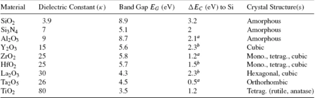
Figure 1.1 Different MIM structure (a) sandwich MIM[5] (b)laminate MIM structure[6]………7
Figure 1.2 TEM micrograph of a assembly of 6-nm as-synthesized Fe50Pt50 particles deposited from a hexane/octane dispersion on SiO-coated copper grid nanodot (B) Replacing oleic acid/oleyl amine with hexanoic acid/hexy-lamine. (C) HRSEM image after annealed at 560℃ for 30min under N2 gas. (D) High resolution TEM image of Fe52Pt48 annealed at 560℃ for 30min.[14]………..7
Figure 1.3 Schematic figure of SAND method………8
Figure 1.4 Hysteresis loop………8
Figure 2.1 Sketch of a quantum box embedded in a matrix………16
Figure 2.2 Schematic presentation of the wavefunction altered with magnetic field in quantum wells (a) under magnetic field (b)under electric field and magnetic field………16
Figure 2.3 Five quantum wells with width 2nm, spacing 2nm, depth 1.0eV with ky=0……….17
Figure 2.4 Probability in center well with different spacing in well width 2nm, well depth 1.0eV……17
Figure 2.5 Probability in center well with different well width in well spacing 2nm, well depth 1.0eV………..18
Figure 2.6 Probability in center well with different effective mass in well spacing 2nm,well width 2nm, well depth 5.0eV………18
Figure2.7 The magnetic field can suppress the tunneling probability more effectively with small electron mass………..19
Figure 2.8 The magnetic field can suppress the tunneling probability more effectively with large bias voltage………19
barrier height………..20
Figure 2.10 The magnetic field can suppress the tunneling probability more effectively with wider barrier width………...20
Figure 3.1 The process flow(a)stpe1 (b)step2 (c)step3 (d)step4 (e)step6………25
Figure 3.2 Vibrating Sample Magnetometer (VSM) structure……….26
Figure 3.3 Transmission electron microscope(TEM) morphology of cross section (a)cross structure (b)scale 20nm(c)scale 5nm………27
Figure 4.1 XRD pattern of FePt thin film with different annealing temperature for 30min (a)400℃ (b)500℃ (c)600℃ ………..37
Figure 4.2 Magnetic hysteresis loop of FePt thin film parallel magnetic field with different element ratio………38
Figure 4.3 Magnetic hysteresis loop of FePt thin film fabricate on different underlayer………..38
Figure 4.4 Magnetic hysteresis loop of MND MIS capacitor after magnetic annealing 700℃ 60 min.………40
Figure 4.5 J-V ofmagnetic FePt nanodot MIS capacitor with different Al top electrode area…………41
Figure 4.6 Ohmic Conduction Fitting (a)accumulation mode (b)depletion mode………..42
Figure 4.7 Schottky emission fitting (a)J-V (b) the Schottky relationship of ln(J/T2) verse 1/kT...43
Figure 4.8 Extract slop from Fig.4.7(b)………...44
Figure 4.9 Frenkel-Poole emission fitting (a)J-V (b) Frenkel-Poole thermal relationship………..45
Figure 4.10 Extract slop from Fig.4.9(b)……….46
Figure 4.11 J-V characteristic of MIS capacitor compares with FePt MND and non-MND………46
Figure 4.12 SCLC fitting (a)accumulation mode (b)depletion mode………...47
Figure 4.13 Tunneling fitting (a)accumulation mode (b)depletion mode ………48
Figure 4.14 Leakage current mechanism fitting (a) accumulation mode (b) depletion mode………….49
Figure 4.15 Current density with 20V constant voltage stress during 10000 second………..50
Figure 4.17 C-V with constant voltage stress 20V during 10000s………..52
Figure 4.18 FePt MND capacitor C-V characteristic with thermal stress at (a)1MHz (b)1kHZ……….53
Chapter 1
Introduction
1.1 Overview of Metal-insulator-Metal (MIM) capacitor
The metal-insulator-metal (MIM) capacitor is one of the most important passive
device in radio-frequency and analog signal IC applications. The dramatic increase in
wired and wireless communications has triggered the demand on MIM capacitors with
low parasitic, high quality factor, and low voltage coefficients [1].
In the conventional metal-insulator-Si-substrate (MIS) has been widely used for
a long time. Comparing with the simple oxide as a dielectric, the most benefit for
high-k dielectrics is the leakage current density reduction by several orders of
magnitude at the same Equivalent oxide thickness (EOT). On the other hand, Metal
has higher carrier concentrations and lower resistance can replace Si-substrates to
reduced the contact resistances and raise the storage charge comparing to normal MIS
structure. Due to device shrinkages and the charge storage in conventional MIS
structure is hard to meet the requirements, the MIM structure is expected to substitute
applied in IC industry.
With the trend of downscaling of MIM capacitors for high capacitance density,
thickness of dielectrics must reduce and thus increase undesired leakage current and
poor voltage linearity. To go in for high capacitance density and scaling down
device, high-k dielectrics have investigated for a while, such as Ta2O5 [2], HfO2 [3],
Al2O3 [4]. Table 1.1 show the comparison of relevant properties for some high-κ
sandwich [5] or laminate structures [6](Fig.1.1), had been investigated. In addition,
researches of nanodots embedded in insulators shows high dielectric permittivity
value in nanoscale MIM device [7], which has advantage in increasing permittivity
and decreasing device scale.
1.2 Introduction to FePt magnet nanodot (MND)
1.2.1 FePt magnet nanodot fabrication
The synthesis and assembly of small hard magnetic magnetic nanodot (MND)
have attracted more and more attention because of their potential applications in
ultrahigh-density magnetic recording [8], ferrofluids [9], advanced nanocomposite
permanent magnets, [10][11] and even biological microsystems. The chemically
ordered FePt face-centered-tetragonal (fct) phase is an excellent candidate for those
applications due to their good chemical stability , high magnetocrystalline anisotropy,
Ku (~108 erg/cm3)[12][13] and and saturated magnetization Ms=13.8 kG. There are two way to prepare the FePt magnet nanodot in generally:
The first method, invented by Sun. [14], it used a combination of oleic acid and
oleyl amine to stabilize the monodisperse FePt colloids and prevent oxidation. The
synthesis is based on the reduction of Pt(acac)2 (acac-5-acetylacetonate,
CH3COCHCOCH3) by a diol and the decomposition of Fe(CO)5 in high-temperature
solutions. The use of diol or polyalcohol (for example, ethylene glycol or glycerol) to
reduce metal salts to metal particles is referred to as the “polyol process” [15]. If
Pt(acac)2 to Pt metal. Thermal decomposition of Fe(CO)5 has been used to produce Fe
particles . Both chemical reactions were initiated together in the presence of oleic acid
and oleyl amine, providing a convenient route to monodisperse FePt nanoparticles [16]
as show in Fig.1.2
The FePt particle size can be tuned from 3 to 10 nm by first growing 3-nm
monodisperse seed particles in situ and then adding more reagents to enlarge the
existing seeds to the desired size. These particles are isolated and purified by
centrifugation after the addition of a flocculent (for example, ethanol) and can be
redispersed in nonpolar solvents in a variety of concentrations. When the FePt
colloids are spread on a substrate and the carrier solvent is allowed to slowly
evaporate, FePt nanoparticle superlattices are produced.
The another way is developed by Cheng-Kuan YIN [17], FePt MND films that
were formed by a novelself-assembled nanodot deposition (SAND) method(Fig.1.3),
where FePt pellets lay on the SiO2 target to cosputtered in the high-vacuum RF
magnetron sputtering equipment. The target ratio of FePt/SiO2 was defined as ratio of
the area of FePt pellets to the suface area of a SiO2 target where the FePt pellets are
placed. Therefore, the target ratio of FePt/SiO2 is controlled by changing the mumbers
of FePt pellets. To obtain uniform dot size ans dot density, the silicon substrate was
rotated at a rate of 75 rpm during sputtering process. As-deposited FePt nanodots
were self-assembled into a chemically disordered face-centered cubic (fcc) phase.
Thermal annealing converts the chemically disordered FePt nanodots into chemically
ordered fct ferromagnetic FePt nanodots. Annealing was performed in a high-vacuum
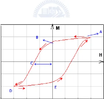
1.2.2 Hysteresis loop
When ferromagnetic material is under applied magnetic field, its induced
magnetic field is raise according to applied field increasing from zero to maximum.
(Fig.1.4)Up to some value, ferromagnetic magnetic field keeps steady whether applied
magnetic raise, this value is saturation magnetization (A-point). And then decreasing
applied field, the induced magnetic field is also decreasing by another path, not along
previous magnetization curve to zero applied field. This is hysteresis phenomenon,
and B point is remanence magnetization. At this point, a reverse magnetic direction
field is required to demagnetize (C point),this value is coercivity (Hc) or coercive
field intensity. As same effect to positive magnetic direction, a reverse magnetic
direction also let ferromagnetic material saturated at D point, and when applied force
decreasing to zero (E point), the magnetization curve becomes a loop form. The curve
is called magnetic hysteresis loop.
1.3 Motive
In past, magnetic material, such as Fe,Co,Ni and their compound ,is regard as
pollution in front-end stage fabrication in semiconductor area. There are seldom
experiments on magnetic nanodot applied in tradition MIS capacitors. We want to
expand to the magnetic material application, and explore to the effect on electric
properties. We select FePt as our magnetic nanodot material, because it is good
chemical stability, high magnetocrystalline anisotropy, and large saturated
magnetization. And the superlattice structure was used to embedded FePt magnetic
nanodot in traditional MIS capacitor. Layers with magnetic field dependent
1.4 The organization of this thesis
In briefly described this thesis, Chapter 1 depicts the background of research and
motivation. In Chapter 2, the simulation was used to model the physics mechanism
about magnetic material in dielectric layer. Chapter 3 describes the experiment and
structure of the capacitor and introduces measurement equipment. Chapter 4 is the
result of electric measurement, and material analysis. Chapter 5 summarizes the
conclusions and contributions of this thesis, and provides the suggested directions for
Figure 1.1. Different MIM structure
(a) sandwich MIM[5] (b)laminate MIM structure[6]
Figure 1.2. (A) TEM micrograph of a assembly of 6-nm as-synthesized Fe50Pt50
particles deposited from a hexane/octane dispersion on SiO-coated copper grid nanodot
(B) Replacing oleic acid/oleyl amine with hexanoic acid/hexy-lamine. (C) HRSEM image after annealed at 560℃ for 30min under N2 gas.
(D) High resolution TEM image of Fe52Pt48 annealed at 560℃ for 30min.[14]
W TiN Sandwich TiN
(
a
(a) (b)Figure 1.3. Schematic figure of SAND method
Figure 1.4. Hysteresis loop;
A: Saturation Magnetization: maximum M measured B: Remanent Magnetization : M at H=0
C: Coercive Field: Field at which M//H changes sign D: Saturation field
Chapter 2
Experimental details
2.1 Introduction to quantum confinement
The quantum confinement effect can be observed once in the quantum well,
quantum wire, or quantum dot which magnitude are the same as the wavelength of the
electron wavefunction. When structures scale down to nanodscale, their electronic and
optical properties deviate substantially from those of bulk materials. A particle
behaves as if it was free when the confining dimension is large compared to the
wavelength of the particle. During this state, the bandgap remains at its original
energy due to a continuous energy state. However, as the confining area decreases and
reaches a certain limit, typically in nanoscale, the energy spectrum turns to discrete.
As a result, the bandgap becomes size dependent.
Specifically, the effect describes the phenomenon results from electrons and
electron holes being squeezed into a dimension that approaches a critical quantum
measurement, called the exciton Bohr radius. In current application, a quantum dot
such as a small sphere confines in all three dimensions, a quantum wire confines in
two dimensions, and a quantum well confines in one dimension.
The advances in semiconductor technology allow one to go further and fabricate
heterostructures in which all existing degrees of freedom of electron propagation are
quantized. These are so called quantum-dots, systems are like artificial atoms and they
2.2 Wave functions and energy levels in quantum dots
Quantum-dot is fabricated heterostructure in which all existing degree of
freedom of electron propagation are quantized. When considering the spectrum of a
zero-dimensional system, we have to study the Schrödinger equation with the
confining potential, which is a function of all three coordinates and confines the
electron in all three directions [19]. The simplest potential type is
dot dot the the outside inside z y x V ⎩ ⎨ ⎧ ∞ + = 0 ) , , ( (2.1)
Where the dot is restricted by the conditions 0≤x≤Lx,0≤ y ≤Ly,0≤ z≤Lz. (Fig.2.1) The solutions of the Schrödinger equation is
(
)
z y x z y x n n n L rzn L yn L xn L L L z y x 1 2 3 ,, sin sin sin
8 , , 3 2 1 π π ψ = (2.2) ⎟ ⎟ ⎠ ⎞ ⎜ ⎜ ⎝ ⎛ + + = ∗ 322 2 2 2 2 2 1 2 2 , , 2 3 2 1 z y x n n n L n L n L n m E h π (2.3)
Thus we obtain threefold discrete-energy levels and wave functions localized in
all three dimensions of the quantum dot. The similarity with atoms is seen another
case of spherical dot, the potential is
R r R r for for V r V b > ≤ ⎩ ⎨ ⎧ = 0 ) ( (2.4)
From quantum mechanics, it is known that under spherical symmetry the
solutions of the Schrödinger equation can be expressed by the separation of angular
and radial dependences in the form
(
θ φ)
( ) ( )
θ φψ r, , =R rYl,m , (2.5)
, which are the spherical coordinates, the well-known spherical functions, l and m are
z. The Schrödinger equation is
( )
V( ) ( )
r r E( )
r r r m eff χ χ χ = ⎥ ⎦ ⎤ ⎢ ⎣ ⎡ + ∂ ∂ − 2∗ 2 2 2 h (2.6) Whereχ( )
r =rR( )
r , 2 2 (1 ) ) ( ) ( r l l r V r Veff = +h − (2.7) As a result of spherical symmetry, the problem reduces formally to aone-dimensional equation. The energy is a function of two quantum number n and
momentum quantum number l, if l=0
(
)
r R R r E V m k E m k r e B r r k A r b b w r K w b > < ⎪ ⎪ ⎩ ⎪⎪ ⎨ ⎧ − = = = ∗ ∗ − h h 2 2 sin ) ( ψ (2.8)At r=R, equations are similar to those studied for one-dimensional problem. We
can find an equation (2.9) for the energy
w b w k V m R k =± ∗ 2 sin 2 h (2.9) The root shows that a level exists inside the spherical well if
2 2 2
8m R
Vb≥ π ∗h (2.10) Thus, eq(2.10) quantifies that a potential well must be large enough or deep
enough to confine the electron.
If l>0, the problem can be analyzed for a large depth of the well. In this case the
radial wave functions have the form
) ( 2 ) ( 2 1 k r J r k r R w l+ = π (2.11) ,where are the bessel function. The roots of the bessel function give us
the following series of the energy levels in quantum dots. )
(r
2.3 Magnetic field in quantum mechanics
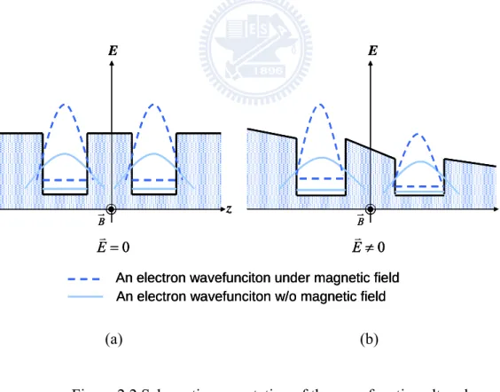
In this section, it is to discuss the quantum structure with magnetic field in
quantum electromagnetism. Electron behavior in magnetic field can be described by
Schrödinger equation. From the development of formula, quantum confinement and
charge localization restrict the charge distribution and improve the insulating behavior
(Fig.2.2).
2.3.1 Schrödinger equation with magnetic field [20][21]
The classical Hamiltonian function appropriated for a charged particle (charge q)
acted on by external electric and magnetic fields in three dimensions is given by
(
ˆ ( , ))
( , ) 2 1 2 t r q t r qA p m Hclassical = − + φ (2.12)The corresponding quantum mechanical Hamiltonian is obtained by replacing the
momentum variable by its operator counterpart, thereby giving the Schrödinger
equation ) , ( ) , ( ˆ ) , ( ˆ r t t i t r E t r Hψ ψ ψ ∂ ∂ = = h (2.13) where
(
ˆ ( , ))
( , ) 2 1 ˆ p qA r t 2 q r t m H = − + φ (2.14)The classical equations of motion depended on the E and B fields are obviously
invariant under any gauge transformation, so the original Hamiltonian is replaced by
) , ( ) , ( )) , ( ) , ( ˆ ( 2 1 ˆ 2 f r t t q t r q t r f q t r qA p m H ∂ ∂ − ′ + ∇ − − = ′ φ (2.15) whereB(r,t)=∇×A(r,t) ) , ( ) , ( ) , ( A r t t t r t r E ∂ ∂ − −∇ = φ
For a constant magnetic field B in z-direction, in terms of potentials φ and Ar, for the interaction of an electron with charge -e and massμ ,we can take
Ar =− rr×Br
2 1
(2.16)
Then, the Hamiltonian from eq.(2.14) can be written as
(
)
2(
2 2 2 ) 2 ( 2 1 ˆ ˆ 2 2 ˆ ˆ P e p A A p eB x y H = + ⋅ + ⋅ + v +)
μ μ μ (2.17)The Schrödinger equation takes the form
ψ ψ φ ψ μ ψ μ ψ μ c A e r E e A c ie ⋅∇ + + = − ∇ − ( ) 2 2 2 2 2 2 2 r h h (2.18)
And manipulating the 3rd term,
( )
[
( )
]
(
ψ μ ψ μ ψ μ 8 8 8 2 2 2 2 2 2 2 2 2 2 2 2 2 y x c B e B r B r c e B r c e + = ⋅ − = × r r r r)
(2.19)For a free electron in a static magnetic field, the electron is confined by the
potential given by (2.19). This is a 2D harmonic potential, and the allowed energy
levels are given by equal spacing according to the harmonic oscillator solutions.
These levels are called Landau levels. Depending on both the Landau quantum
number N and the magnetic field B, the Lorentz force leads charged carriers to
classically describe circular orbits with a cyclotron orbit radius RN [22]
2 2 ) 1 2 ( N l RN = + (2.20) where B eB l 0 256Α = = h (2.21)
2.3.2 Magnetic field induce quantum confinement
Quantum confinement is another notable issue in magnetic field, since it is
strongly related to the Kondo effect [23] and Anderson localization [24], but no
microscopic dynamical mechanisms of this phenomenon have yet been understood in
detail. However, some experiments prove this phenomenon indirectly, with increasing
structure increases. Another evidence reveals magnetic field induced electric
polarization, charge localization, and insulating behavior [25].
2.4 COMSOL simulation
In this section, we use COMSOL Multiphysics, a simulation of any
physics-based system, to simulate the situation of magnetic field effect on multi-wells
confined electron. And supposed the constant magnetic field in z-direction like section
2-3-1, we modify eq. (2.19) in Cylindrical coordinates
) , ( ) , ( ) , ( 4 2 ) , ( 2 2 2 2 2 2 2 2 2 2 2 z Eu z V z u B e eBl l m z u z m ρ ρ ρ ρ ρ ρ ρ ρ ρ ⎟⎟⎠ + = ⎞ ⎜⎜ ⎝ ⎛ + + + ⎟⎟ ⎠ ⎞ ⎜⎜ ⎝ ⎛ ∂ ∂ + ∂ ∂ + ∂ ∂ − h h h h where ψ(x,y,z)=exp(ilφ)u(ρ,z) (2.22)
As description of top formula, with the magnetic field increase, the electron will
more easily be confined in the potential wells due to the additional parabolic potential
term from magnetic field. Fig.2.3 is the simulation result of 5 quantum wells with
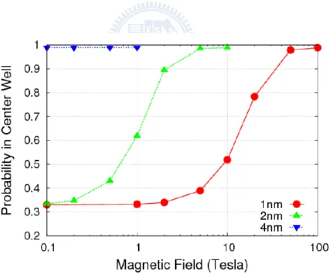
width of 2nm, spacing of 2nm, depth of 1.0eV, with the magnetic field increase, the
profile of probability density function is narrowing to represent the confinement effect.
Altering other parameters, to increase spacing and well width, the probability in
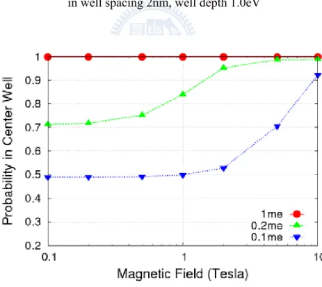
center well is increasing.(Fig.2.4,2.5). Moreover, larger effective mass shows lower
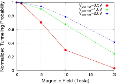
tunneling probability and better field confinement in Fig.2.6 Besides, the magnetic
field in transverse direction suppressed the tunneling probability more efficiently for
lower effective mass, lower barrier height, higher bias voltage and wider barrier
width(Fig.2.7,2.8,2.9,2.10), this phenomena were from the relation of two constants
C m eB c = ∗ ω (cyclotron frequency) (2.23)
( )
[
]
∫
− ∗ ≈ m E x U dx / 2Figure 2.1 Sketch of a quantum box embedded in a matrix z E 0 = Ev B E z B 0 ≠ Ev
An electron wavefunciton under magnetic field An electron wavefunciton w/o magnetic field
z E 0 = Ev B E 0 = Ev B E z B 0 ≠ Ev E z B 0 ≠ Ev
An electron wavefunciton under magnetic field An electron wavefunciton w/o magnetic field An electron wavefunciton under magnetic field An electron wavefunciton w/o magnetic field
(a) (b)
Figure 2.2 Schematic presentation of the wavefunction altered
with magnetic field in quantum wells
Figure 2.3 five quantum wells with width 2nm, spacing 2nm, depth 1.0eV with ky=0
Figure 2.4 Probability in center well with different spacing
Figure 2.5 Probability in center well with different well width
in well spacing 2nm, well depth 1.0eV
Figure 2.6 Probability in center well with different effective mass
Figure 2.7 The magnetic field can suppress the tunneling probability more
effectively with small electron mass
Figure 2.8 The magnetic field can suppress the tunneling probability more
Figure 2.9 The magnetic field can suppress the tunneling probability more
effectively with lower barrier height
Figure 2.10 The magnetic field can suppress the tunneling probability more
Chapter 3
Device Structure and Fabrication
In this chapter, first, describe the experiment process with magnet nanodoat
(MND) in capacitor mentioned and their fabrications are described in 3.1. Material
analysis and electric measurement were introduced in 3.2.
3.1 Magnetic nanodot capacitor Fabrication
(Fig.3.1)Step1. Preparation of Substrate with buffer oxide.
2-inch p-type single crystal silicon wafers with (100) orientation were used
as the starting materials(10-15Ω-cm). After an RCA initial cleaning procedure.
Si wafers were grown with 10-nm-thickness thermally grown SiO2 in steam
oxygen and hydrogen ambient at 900°C. the SiO2 layer is play a role of
insulating layer avoiding current leakage from the Si substrate.
Step2. FePt magnetic nanodot layer
Magnetic nanodots are formed by RF magnetron sputter. In this step , we
use self-assembled nanodot deposition (SAND method) [26], our target is SiO2
with FePt pellet, flow 8 sccm Ar gas and drive power 50W and deposition rate is
less than 0.1 Å. Low power and low pressure is necessary to control the nanodot
to form within SiO2 layer and exactly in thickness 10nm. Another comparison
sample, embedded in Co nanodot.
Step3. Preparation of interlayer insulator block oxide .
Power descend to 50W to drive the plasma to pure SiO2 target for lower
deposition rate in order to grow only 3nm thickness SiO2 as block oxide
between FePt magnetic nanodot layer. Block oxide can avoid FePt magnetic
nanodot diffusing.
Step4. Cycle deposition for superlattice structure..
After setp3, repeat step 2 and step 3 in seven cycles for superlattice
structure.
Step5. Vacuum annealing .
Vacuum annealing under pressure 5×10⁵ Pa, 700℃, 30min. This step
transforms FePt fcc structure to fct structure (L10). During the
post-heat-treatment, the heat is supplied only from the bottom side of the
substrate. For a given annealing temperature and time, the quantity of heat
transferred to the FePt-dot layer is larger for a thin 2.5 nm block oxide as
compared to that for a thicker 10 nm block oxide. This results into an
increase in the size of the nanodots in the sample with a thinner block oxide.
The core of the as-formed FePt nanodots was always preserved in the metallic
state. Possibly, the high vacuum ambient during postannealing, which is
inevitable to transform the as-grown fcc structured FePt nanodots which is
nonmagnetic into the magnetically hard L10 structured one, highly promotes
the release of oxygen from the metal oxides of FePt nanodots via reduction
reaction. This leads to not only an increase in the fraction of metallic Fe and Pt
at the periphery of FePt nanodots, but also the formation of a high quality
Step6. Preparation of top electrode and bottom electrode
In order to define electrode area on wafer, we use shadow mask was used
to paste on wafer surface and coat Al 400nm by thermal coat. Top electrode
size is from 0.00504cm2~0.0003cm2. Bottom electrode is also Al 400nm back-coating on wafer.
3.2 Material analysis and Electric measuremen
t
The magnetic moment is measured by Vibrating Sample Magnetometer (VSM)
(Fig.3.2). When a sample is under single direction magnetic field, it will has induced
magnetic moment. If sample vibrates like sin wave mode under magnet winding, the
magnetic flux changes with vibration. It was detected by another magnet winding,
and induced signal voltage. This signal is in proportional to magnetic moment and
measure magnetic characteristic. In VSM, every sample is under addition magnetic
force 30kOe (±15kOe) and vibration frequency 80Hz. The smallest detective magnet is 5×10⁻⁵ erg/Oe. Therefore Coercive field and saturation field can be known from
magnetic hysteresis loop.
Structure and morphologies of cross section were confirmed by
transmission electron microscope (TEM) in Fig.3.3 X-ray diffraction (XRD) was
employed to identify the crystal structure of the nanodot using Cu Kα radiation with
λ=0.5418 nm. And check the components of FePt ratio were estimated by inductively
For electrical measurement, the leakage current-voltage (J-V) curves were measured
by the semiconductor parameter analyzer of model Kethley 4200. The
capacitance-voltage (C-V) curves were measured by the precision impedance meter of
(a) step1:RCA clean and LPCVD 10nm
(b) step2:FePt nanodot with SAND method
(C) step3:Sputter 3nm block oxide
(d) step4:Repeat step2~step3 ,total 8 cycles
Step5: Vacuum annealing 700 ℃
(e) step6: Top and bottom coat Al electrode
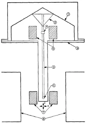
Fig. 3.2 Vibrating Sample Magnetometer (VSM) structure (1) Loudspeaker transducer (2) conical paper cup support (3) drinking straw (4) permanent magnet reference sample (5) sample (6) reference coils (7) sample coils (8) magnet poles (9) metal container to allow evacuation.
(b)
Al
Al
Si substrate
Oxide 10nm
FePt MND 10nm
Al
Al
Si substrate
Oxide 10nm
FePt MND 10nm
(a)
(c)
Figure 3.3 Transmission electron microscope(TEM) morphology of cross section (a)cross structure (b)scale 20nm (c)scale 5nm
Chapter 4
Experiment Results and Discussion
4.1 The magnetic FePt film properties
In order to confirm FePt to have magnetic properties, we try to find the best FePt
magnetism characteristic. We change different atomic concentration Fe:Pt ratio in the
way of altering film thickness during sputtering, try different annealing condition,
measure the magnetization moment by VSM and compare with paper [27] in L10 fct
lattice structure in XRD see Fig.4.1 After annealing in vacuum, the FePt lattice
structure transforms from original fcc to fct. The annealing temperature need to reach
to 600℃ to transform its structure, and the evidence is that peaks appear after the
600℃ 30 minutes annealing. However, below 600℃ it stays fcc state without any
direction of fct structure. Fig.4.2 is the VSM of the different Fe to Pt ratio with vacuum annealing 600℃ 30 minutes, the magnetic property of FePt is not only
decided by its fct structure, proper ratio of the number of Fe and Pt atoms is also the
major factor. Beside, the under layer and annealing temperature also play an important
role to arrange the Fe and Pt in correct order and with large magnetic anisotropy.
Fig.4.3 is the effect of magnetism on different under layer. For Pt as being the buffer
layer, it can order the growth of FePt fcc phase extended into the L10 FePt (001)
magnetic layer [28], which can be not only exhibited a large parallel magnetic field
but also used to bottom electrode. Pt under layer has another advantage for high
stability in heat treatment and metal addition [29]. On the topic of Fe:Pt ratio, we
quantitatively determine by layer thickness, and exactly analysis component ratio by
elemental percentage of Fe:Pt = 48:52 has large coercivity and saturation
magnetization. Fig 4.4 is the magnetic hysteresis loop of FePt MND MIS capacitor
after magnetic annealing 700℃ 60 minutes. Table 4-2 is the physical quantity value of
magnetic field.
4.2 Properties of magnetic nanodot MIS leakage characteristics
To recognize the effect of magnetic nanodot in capacitor, we measure the
characteristic of current density and voltage. Fig.4.5 shows the current density verse
voltage of magnetic FePt nanodot MIS capacitor with different Al top electrode area.
Asymmetry curve reveals different leakage mechanism in two current directions.
When positive bias force on 3×104 μm2
Al top electrode, the leakage curve is flat to
9.5×10⁻⁵ A/cm under ±10V. This is the value that electrons overcome the 10nm block oxide barrier on Si. Beyond +10V, leakage current density increases quickly to 10
A/cm and is not breakdown even under high voltage strength 100V. In this region,
MIS capacitor with FePt MND (magnetic nanodot) is with high leakage current which
is unusual in MIS capacitor without MND. On the other way, reverse bias force on top
electrode, the leakage current also has the same behavior in first -10V. If negative bias
is larger than this value, the leakage current mechanism is different. To recognize the
leakage current mechanism of the magnetic nandot capacitor, we take five different
mechanisms into consideration (see Table 4-3) [30].
4.2.1 Ohmic Conduction Fitting
For the leakage current at very low field (~±10V in MND FePt capacitor), the
leakage current in accumulation mode increases linearly with the increase of voltage
conduction mechanism, which describes the situation of low voltage and high
temperature, current is carried by thermally excited electrons hopping from one
isolated state to the next. Ohmic conduction takes place when the injected carrier
density is far less than the thermally-generated carrier density, which
thermally–generated carriers are dominant in conduction. The relation can be
expression in (4-1) ⎟ ⎠ ⎞ ⎜ ⎝ ⎛− = T c aV J exp (4-1)
Where a, c is constant, V is applied voltage and T is the absolute temperature. We
can also observe from Fig.4.6(b), a plot of J verse V yields a straight line within +10V
(depletion mode). When applied voltages are between 10 to -10V, the carriers
transport mechanism is Ohmic conduction.
4.2.2 Schottky Emission Fitting
Fig.4.7(a) shows the Schottky emission fitting for FePt nanodots MIS capacitor
in accumulation mode. The linear relationship of ln(J/T2) versus V1/2 curve was
obtained in the range of -25V to -40V, which gives the slope of 2.504 eV(m/V)1/2 with a goodness of fit functions of 0.9965. The fitting curve in depletion mode is in the range of 13V~20V. Schottky emission mechanism is which leakage current
contributed by the carriers that overcome the barrier height between electrodes and
dielectric layers, it is also called thermionic emission because the key point is hot
carrier emission jump across barrier height. The formula is below:
⎥ ⎥ ⎦ ⎤ ⎢ ⎢ ⎣ ⎡− − = ∗ kT qE q T A J 2exp (φB /4πε) (4.2)
Where A* is the Richardson constant, k is the Boltzmann’s constant, T is the
absolute temperature (K), E is the applied external electric field , e is electron charge,
ε is the permittivity in vacuum, and φBis corresponding to the barrier height between
metal/dielectric. Fig.4.7(b) is the thermal relationship of ln(J/T2) and 1/kT, however,
extract the slop verse sqrt voltage in Fig.4.8, nonlinear relation between -25 to -49V
demonstrates that the leakage current is independent of temperature. Indirectly prove
that Schottky emission conduction is not the main mechanism in high field strength.
4.2.3 Frenkel-Poole Emission Fitting
Fig.4.9(a) is Frenkel-Poole emission fitting on reverse bias applied on top Al
electrode. Frenkel-Poole emission describes the process for carriers to overcome the
barriers resulted from the defect states in dielectric layer, and the barrier lowering is
lower in Schottky emission and tunneling. Because its conduction process depends on
carrier trapped and detrapped behavior, electric field plays a more important factor
than temperature in this mechanism which is verse in Schottky emission. The
relationship can be written as following:
(
)
⎟ ⎟ ⎠ ⎞ ⎜ ⎜ ⎝ ⎛− − = kT qV q BV J exp φt /πε (4.3)Where B is material constant, φt is trap barrier height, and other parameters
are the same as those in Schottky emission. The goodness of fitting curve is reach
0.99 in the range of -12V~-20V, and Fig.4.8 shows the thermal relationship of
Frenkel-Poole emission, from the slop of ln(J/V) and 1/kT (Fig.4.9(b)), we can figure
out the barrier height is 0.049eV from Fig.4.10. It can explain the main mechanism
onlyin oxide but also produced by embedded FePt nanodot. The magnetic of nanodot
may provide another force to induce electron conduct through adjacent traps in
quantum mechanics effect. That is the reason that capacitor with FePt nanodot has
high breakdown voltage nearly 49.2V when reverse bias force on top electrode, which
is extremely large than general in dielectric thickness ~34nm (see TEM section
monograph in Fig 3.3), it also reveals that electric field strength in dielectric layer is
large to 14MV/cm, MV cm nm V t V E ox / 14 34 2 . 49 = = = (4.4)
Compare with non-MND capacitor in Fig.4.11, it shows the J-V characteristic of
MIS capacitor compares with FePt MND and non-MND in 38nm oxide thickness.
Obviously, with the same oxide thickness, magnetic nanodot FePt enhances the
electric field intensity in oxide and high voltage breakdown.
4.2.4 Space Charge Limited Current Fitting
Another leakage mechanism is space charge limited current (SCLC), which is
attributed to defects in dielectric under high electric field. After charge injection from
an electrode, the space charges are formed by trapped carrier. The major SCLC
divided into two parts in following:
1 1 8 9 8 9 3 2 3 2 >> << ⎪ ⎪ ⎩ ⎪⎪ ⎨ ⎧ = θ θ εμ εμ θ d V d V J (4.5)
J is current density ,θ is the ratio of free electron to trapped electron ,εis
case is proportional to the square of the applied voltage. The fitting result in Fig.4.12,
the slop in accordance with SCLC mechanism must be 2, but our fitting slop is in
proportional line with slope 0.94 from -0.3 to -11V, is less similar fitting in
comparison to Ohmic conduction. But in the depletion mode, the bias large than +13V
has large fitting goodness 0.991 and slop 1.75 for slop lnJ verse lnV. In high electric
field condition, the gate leakage current in the deep depletion region is mainly limited
by the generation of minority carriers via the interface states and bulk traps in the
depletion region [31], which results in a lower saturation current level under positive
bias. In the standard capacitor without FePt NMD, its leakage current saturated at
10-6A over 40V.
4.2.5 Tunneling Fitting
Electron tunneling through thin dielectric layer is another conventional way to
conduction electron, Fig.4.13 is the tunneling fitting curve, which is evidently to
observe the relationship of following formula between -13V to before breakdown:
( )
⎟ ⎠ ⎞ ⎜ ⎝ ⎛ − ∝ ⎥ ⎥ ⎦ ⎤ ⎢ ⎢ ⎣ ⎡ − ∝ ∗ V b V q q m J B exp 3 2 4 exp 2 2 / 3 2 ξ φ ξ h (4.6)Where ζ is the electric field in insulator, m* is the effective mass, ψB is the barrier height, and V is the applied voltage. We can calculateψB is 1.07eV in
accumulation mode. Obviously, the leakage current of FePt NMD capacitor is not
only direct tunneling under high electric field but also transport carriers by jumping or
trapping in FePt NMD layer.
Above of all, the leakage mechanism of MND is apparent difference in
(<10V), the carrier transition is Ohmic conduction because FePt nanodot embedded in
oxide which made dielectric metalize in carrier conduction properties. Beyond -10V,
its current density rapidly rise than before and keep high current density in high field
strength until to 49V breakdown. This phenomenon is resulting from FePt MND
induced parallel magnetic which attract carrier and restrict their conduction path by
quantum confinement localization [32]. The mechanism makes leakage current
behaviors obey to like Frenkel-Poole emission and tunneling compound features in
high field strength in accumulation mode. FePt nanodots in capacitors are the
quantum well location which potential lower than oxide. Additionally, the
self-induced parallel magnetic field suppresses the tunneling between adjacent wells
in FePt nanodot/SiO2 layer by layer structure, which results in the electric field
strength must be larger than standard situation in order to prompt carriers tunneling.
These reasons make carrier conduction is like metallic Ohmic conduction mode in
low field, trapped or detrapped mode in high electric field. In positive bias applied on
top electrode (depletion mode), the leakage current mechanism is also like Ohmic
conduction in 0V~+10V, +10~14V is dominated by Frenkel-Poole emission and
higher 14V, it is space charge limited current and restricted by minority carrier
concentration from depletion region, keep static leakage level until to +100V. Fig.
4.14 is the total fitting result of FePt MND capacitor in accumulation mode and in
depletion mode, respectively.
4.3 The Voltage and Temperature Effect of FePt MND Capacitors
The properties of stability, precision, and endurance are important for
capacitors. In this section, we investigate the stress behavior on electrical properties
stress.
4.3.1 Voltage Stress on FePt MND Capacitor
Fig.4.15 shows the leakage current density under +20V stress verse stress time
for FePt NMD capacitor. Fig.4.16 and Fig.4.17 show the J-V and C-V behavior after
constant voltage stress at 20V for various stress time. In generally, the capacitance
density will increase under lower electric field with the increase of stress time since
the injected charges pile up in dielectric thin film near top electrode, at meantime , the
charge pile-up cause lower electric field to reduce the leakage current at lower voltage
because of electron trapping phenomenon in insulator layer. [38] Conversely, an
excessive voltage could increase the charges-injected energy largely to damage the
dielectric and generate hole traps which decrease the capacitance density and increase
the leakage current, respectively. [39]
These phenomena existing in FePt MND capacitor are different. After high
voltage stress at 20V, the leakage current keeps static values of 4.5×10⁻⁵ A and 5.8×10⁻⁵ A at -10V and +10V, respectively, during stress time (Fig.4.17). A slight variation of leakage current is that leakage current density reduced with increasing
stress time in the range from -10 to -15V. FePt nanodots embedded in oxide may
attract charge pile-up, it could result from FePt providing a lower potential position to
receive the charges and confinement these charges that reduce the leakage current
with increasing stress time. The capacitance density increases with the increase of
stress time since the injected charges pile up at FePt nanodots and oxide matrix
interface. After the existing traps were filled by the injected electrons, electrons
tunneled through the dielectric layer easily so that few electrons were trapped but
many new traps were generated in the bulk of dielectric by the high energy electrons.
due to the piled-up electrons.
4.3.2 Thermal Stress on FePt MND Capacitor
Fig.4.18(a) shows capacitance density of the FePt MND capacitor at 1MHz
from 25℃ to 125℃. After thermal stress, the capacitance density increases with
temperature at 1MHz and more obviously at 1KHz (Fig.4.18(b)). The major reason is
considered to be the interface defect density existed between FePt nanodot and oxide
matrix medium increasing during the thermal stress process. The leakage current
density also affected on thermal stress in depletion mode, it can reveal that FePt
nanodot structure is relatively stable under thermal stress in accumulation mode.
Fig.4.19 shows the effect on current density with thermal stress. In accumulation
mode, current density increases slightly with temperature before breakdown voltage.
In depletion mode, current density increases nearly one order in magnitude beyond +13V on the rise per of temperature per 25℃. It is worth noting that current density
did not rise when temperature exceed 100℃. As mentioned previously, carrier
conduction is major limited by the generation of minority carriers via the interface
states and bulk traps, and the generation and recombination rates of minority carriers
Figure 4.1 XRD pattern of FePt thin film with different annealing temperature for 30min (a)400℃ (b)500℃ (c)600℃
Figure 4.2 Magnetic hysteresis loop of FePt thin film parallel magnetic field with different element ratio
Figure 4.3 Magnetic hysteresis loop of FePt thin film fabricate on different underlayer
Table 4-1 Different element concentration ratio of Fe:Pt measured by ICP-MS
Estimative ratio by thin film thinkness (Å)
Real ratio (ppm) Pt:Fe Pt Fe 25:20 0.7114(26%) 2.0246 (47%) 25:25 0.657(39%) 1.040 (61%) 51:40 2.764(53%) 2.432(47%) 51:40 0.577 (48%) 0.617(52%)
Figure 4.4 Magnetic hysteresis loop of MND MIS capacitor after magnetic annealing 700℃ 60 minutes
Table 4-2 Magnetization value of FePt MND Magnetic hysteresis Physics quantity (unit) Parallel magnetic field Vertical magnetic field Ms(emu) 6.433×10⁻⁴(0.26T) 7.086×10⁻⁴ (0.29T) Mr(emu) 2.457×10⁻⁴ (0.1T) 7.854×10⁻⁵(0.03T) Hs(Oe) 12724.86 13846.89 Hn(Oe) 10271.99 13414.54 Hc(Oe) 968 716.46
Figure 4.5 J-V ofmagnetic FePt nanodot MIS capacitor with different Al top electrode area
Table 4-3 Cnduction mechanisms[30]
Conduction mechanism Characteristic Temperature dependence Voltage dependence V V J 1 ~ ln 2 ⎟ ⎠ ⎞ ⎜ ⎝ ⎛ Tunneling ( ) ⎥⎥ ⎦ ⎤ ⎢ ⎢ ⎣ ⎡ − ∝ ∗ ξ φ ξ h q q m J B 3 2 4 exp 2 / 3 2 None Termionic emission (Schottky emission) ⎥⎥⎦ ⎤ ⎢ ⎢ ⎣ ⎡− − = ∗ kT qE q T A J 2exp (φB /4πε) T T J 1 ~ ln 2⎟ ⎠ ⎞ ⎜ ⎝ ⎛ 2 / 1 ~ lnJ V Frenkel-Poole emission
(
)
⎟⎟ ⎠ ⎞ ⎜ ⎜ ⎝ ⎛− − = kT qV q BV J exp φt /πε T V J 1 ~ ln ⎟ ⎠ ⎞ ⎜ ⎝ ⎛ ln ~V1/2 V J ⎟ ⎠ ⎞ ⎜ ⎝ ⎛ Ohmic ⎟ ⎠ ⎞ ⎜ ⎝ ⎛− = T c aV J exp T V J 1 ~ ln ⎟ ⎠ ⎞ ⎜ ⎝ ⎛ V J ∝ Space-charge-limited 3 2 8 9 d V J = εiμ None ∝V2(a)
(b)
(a)
Schottky emission
1/kT
28
30
32
34
36
38
40
-15
-14
-13
-12
-11
-10
-9
-8
-7
25.0V 30.3V 36.0V 42.3V 49.0Vln (J/T
2) (A
/c
m
2-T
2)
(b)Figure 4.7 Schottky emission fitting
(a)
(b)
Figure 4.9 Frenkel-Poole emission fitting (a)J-V (b) Frenkel-Poole thermal relationship
Figure 4.10 Extract slop from Fig.4.9(b)
Figure 4.11, J-V characteristic of MIS capacitor compares with FePt MND and non-MND
(a)
(b)
(a)
(b)
(a)
(b)
Figure 4.14 Leakage current mechanism fitting (a) accumulation mode (b) depletion mode
Figure 4.15 Current density with 20V constant voltage stress during 10000 second
(a)
(b)
Figure 4.16 J-V with constant voltage stress (a)accumulation mode (b)depletion mode
(a)
(b)
Figure 4.18 FePt MND capacitor C-V characteristic with thermal stress at (a)1MHz (b)1kHZ
Chapter 5
Conclusion and Future Work
5.1 Conclusion
From quantum mechanics, magnetic field has a confinement effect that restricts
the charge distribution and improves the insulating behavior. We take COMSOL as
simulation tool to present this effect and fabricate FePt magnetic nanodots capacitors
to proof this phenomenon.
The capacitor with magntic FePt nanodots has high breakdown electric strength;
its leakage mechanism is different to general non-metal-dot capacitors. In
accumulation mode, tunneling and Frenkel-Poole emission is the main mechanism
because FePt nanodot is a possible trap provider. And magnetic field from FePt
nanodots may make carrier tunnel though dielectric material difficultly that in result
of high breakdown strength.
FePt nanodots existing in dielectric layer also enhance the static dielectric
constant of silicon oxide. The electric polarizability is greatly increased because of the
interface of FePt metal dots and silicon oxide and its magnetic properties. And under
constant voltage stress +20V, the FePt MND capacitor has good characteristic in
5.2 Future Work
In future work, we can research the relationship of MND capacitor with
different magnetic field strength and then progress to discuss the magnetic nanodots
quantum confinement effect in different structure. Verify the role of parallel or vertical
magnetic field in capacitor. Furthermore, this structural possibility for future flash
Reference
Charpter1
[1]International Technology Roadmap of Semiconductors (ITRS), San Jose CA: SIA.
[2] T. Remmel, R. Ramprasad, and J.Walls, “Leakage behavior and reliability assessment of tantalum oxide dielectric MIM capacitors,” in Proc. Reliab Phys.
Symp., 2003, pp. 277–281.
[3] H. Hu, C. X. Zhu, Y. F. Lu, M. F. Li, B. J. Cho, and W. K. Choi “A high performance MIM capacitor using HfO2 dielectrics,” IEEE Electron Device Lett.,
vol. 23, no. 9, pp. 514–516, Sep. 2002.
[4] Y. L. Tu, H. L. Lin, L. L. Chao, D. Wu, C. S. Tsai, C. Wang, C. F. Huang, C. H. Lin, and J. Sun, “Characterization and comparison of high- κ metal–insulator–metal (MIM) capacitors in 0.13 μm Cu BEOL for mixed-mode and RF applications,” in VLSI Symp. Tech. Dig., 2003, pp. 79–80.
[5] Y. K. Jeong, S. J. Won, D. J. Kwon, M. W. Song, W. H. Kim, O. H. Park, J. H. Jeong, H. S. Oh, H. K. Kang, and K. P. Suh, “High quality high-κMIM capacitor by Ta2O5/HfO2/Ta2O5 multilayered dielectric and NH3 plasma interface treatments for mixed-signal/RF applications,” in VLSI Symp. Tech. Dig., 2004, pp. 222–223. [6] H. Hu, S. J. Ding, H. F. Lim, C. X. Zhu, M. F. Li, S. J. Kim, X. F. Yu, J. H. Chen,
Y. F. Yong, B. J. Cho, D. S. H. Chan, S. C. Rustagi, M. B. Yu, C. H. Tung, A. Y. Du, D. My, P. D. Foo, A. Chin, and D. L. Kwong, “High performance ALD HfO2−Al2O3 laminate MIM capacitors for RF and mixed signal IC applications,” in
IEDM Tech. Dig., 2003, pp. 15.6.1–15.6.4.
[7]Z. Liu, T. P. Chen,Y. Liu, M. Yang, J. I. Wong, and Z. H. Cen, “Static dielectric constant of Al nanocrystal/Al2O3 nanocomposite thin films determined by the
capacitance-voltage reconstruction technique”,in Appl. Phys. Lett. 96, 173110 ,2010
[8]D. Weller, A. Moser, L. Folks, M. E. Best, W. Lee, M. F. Toney, M. Schwickert, J.-U. Thiele, and M. F. Doerner, IEEE Trans. Magn. 36, 10~2000.
[9] B. M. Berkovsky, V. F. Medvedev, and M. S. Krakov, Magnetic Fluids:
Engineering Applications ~Oxford University Press, Oxford, 1993.
[10] H. Zeng, J. Li, J. P. Liu, Z. L. Wang, and S. H. Sun, Nature ~London 420,395 ~2002.
[11] M. Watanabe, T. Masumoto, D. H. Ping, and K. Hono, Appl. Phys. Lett. 76, 3971 ~2000.
[13] R. F. C. Farrow, D. Weller, R. F. Marks, M. F. Toney, A. Cebollada, and G. R. Harp, J. Appl. Phys. 79, 5967 ~1996.
[14] S. H. Sun, C. B. Murray, D. Weller, L. Folks, and A. Moser, Science 287, 1989 ~2000
[15] F. Fievet, J. P. Lagier, M. Figlarz, MRS Bull. 14, 29 (1989).
[16] K. S. Suslick, M. Fang, T. Hyeon, J. Am. Chem. Soc. 118, 11960 (1996).
[17] Cheng-Kuan YIN, Mariappan MURUGESAN1, Ji-Chel BEA, Mikihiko OOGANE, Takafumi FUKUSHIMA, Tetsu TANAKA, Shozo KONO, Seiji SAMUKAWA, and Mitsumasa KOYANAGI,” New Magnetic Nanodot Memory with FePt Nanodots”, Japanese Journal of Applied Physics, Vol. 46, No. 4B, 2007, pp. 2167–2171
Chapter 2
[18] Vladimir V. Mitin,Viatcheslav A. Kochelap, Michael A. Stroscio,Quantum
Heterostructures, pp.73-75,Cambridge University Press,1999
[19] Vladimir V. Mitin,Viatcheslav A. Kochelap, Michael A. Stroscio,Quantum
Heterostructures, pp.91-94,Cambridge University Press,1999
[20] Richard W. Robinett, Quantum Mechanics-classical results, modern systems, and
visualized examples, pp.444-449, Oxford University Press,1997
[21] Patrik Fazekas, Lecture Notes on Electron Correlation and Magnetism, pp.19-28, World Scientific Publishing Co. Pte. Ltd. 1999
[22] Petra Denk, Martin Hartung,Martin Streibl, and Achim Wixforth ,Kenneth L. Campman and Arthur C.Gossard, “Magnetic-field-induced charge localization in a high-mobility semiconductor semiconductor superlattice”, Phys. Rev. B 57, number 20,1998
[23] Robert M. White, Quantum Theory of Magnetism,pp.200-204, McGRAW-HILL,1970
[24]Patrick A. Lee, Daniel S. Fisher, Phys. Rev. Lett. 47, 882–885 (1981)
[25] D. V. Khveshchenko,”Magnetic-Field-Induced Insulating Behavior in Highly Oriented Pyrolitic Graphite”, Phys .Rev. Let .87, 206401, 2001
Chapter 3
[26] Cheng-Kuan Yin, Mariappan Murugesan, Seiji Samukawa, Mitsumasa Koyanagi, ”New Magnetic Nanodot Memory with FePt Nanodots ”, Jpn. J. Appl.
Phys., vol.46, no.4B, 2007, pp.2167-2171.
Chapter 4
[27] M. H. Lu, T. Song, and T. J. Zhou et al. ”FePt and Fe nanocomposite by annealing self-assembled FePt nanoparticles”, J. Appl. Phys. 95, no.11, part 2, 2004.
[28] An-Cheng Sun, P.C. Kuo, Jen-Hwa Hsu, H. L. Huang, Jui-Ming Sun, “Epitaxial growth mechanism of L10 FePt thin films on Pt/Cr bilayer with amorphous glass
substrate”J. Appl. Phys. 98 076109, 2005
[29] Toshio Suzuki and Kazuhiro Ouchi, IEEE Transactions on Magnetics, 37, no.4, 2001
[30] S. M. Sze, Kwok K. Ng, Physics of Semiconductor Devices, John Wiley & Sons Inc, 2007, pp.227-236.
[31] Chih-sheng Kuo, Jui-feng Hsu et al. ”High-k Al2O3 Gate Dielectrics”, IEEE
Transactions on electron devices, vol. 51,no. 6, 2004
[32] Takio Hikono, Takashi Matsumura, Atsushi Miura, Yukiharu Uraoka et al. ”Electron confinement in a metal nanodot monolayer embedded in silicon dioxide produced using ferritin protein”, Appl. Phys. Lett. 88, 023108, 2006
[33] M. Gauthie, Engineered Materials Handbook Desk Edition, the materials information society, 1995.
[34] R. Dupree, M. A. Smithard, “The electronic properties of small metal particles: the electric polarizability”, J. Phys. C, vol.5, 1972.
[35] S. Strässler and M. J. Rice, P. Wyder, “Comment on Gorkov and Elishberg’s Result for the Polarizability of a Minute Metallic Particle”,Phys. Rev. B, vol 6, no.7,1972
[36] Vishal Singh, A. R. Kulkarni, T. R. Rama Mohan,”Dielectric Properties of Aluminum-Epoxy Composites”, Jou. of Appl. Poly. Sci., vol. 90, 3602-3608, 2003 [37] Z. Liu, T. P. Chen, Y. Liu, M. Yang et al, ”Static dielectric constant of Al
nanocrystal/Al2O3 nanocomposite thin films determined by the
capacitance-voltage reconstruction technique”, Appl. Phys. Lett. 96, 173110, 2010 [38] R. Bartnikas, “Performance characteristicd of dielectricd in the presence of space
charge”, IEEE Transactions on Dielectrics and Electrical Insulation, vol.4, no.5, 1997
[39] Chi-Chao Hung, Anthony S. Oates, Horng-Chih Lin, Yu-En Percy Chang, Jia-Lian Wang, Cheng-Chung Huang and You-Wen Yau, “An innovative
Understanding of Metal-Insulator-Metal (MIM)-Capacitor Degradation Under Constant-Current Stress,” IEEE Trans. Electron Devices, vol. 7, no. 3, pp. 462-467, Sep. 2007.
[40] S. M. Sze, Kwok K. Ng, Physics of Semiconductor Devices, John Wiley & Sons Inc, 2007, pp.40-45.
Chapter 5
[41] Ji chel Bea, Yun Heub Song, Kang-Wook Lee, Gae-Hun Lee, Tetsu Tanaka and Mitsumasa Koyanagi, “Cell characteristics of a mltiple alloy nano-dots memory structure”Semicond. Sci. Technol. 24,2009,085013