國
立
交
通
大
學
電子物理系
碩
士
論
文
矽奈米元件量子修正理論暨模式應用比較之研究
Modeling of Quantum Mechanical Effects for Nanoscale
MOS Devices with Correction Theory
研 究 生:陳煒昕
指導教授:趙天生 博士
矽 奈 米 元 件 量 子 修 正 理 論 暨 模 式 應 用 比 較 之 研 究
Modeling of Quantum Mechanical Effects for Nanoscale
MOS Devices with Correction Theory
研 究 生:陳煒昕 Student:Wei-Hsin Chen
指導教授:趙天生 博士 Advisor:Dr. Tien-Sheng Chao
國 立 交 通 大 學
電 子 物 理 研 究 所
碩 士 論 文
A Thesis
Submitted to Institute of Eletrophysics College of Science
National Chiao Tung University in partial Fulfillment of the Requirements
for the Degree of Master in Electrophysics July 2006 Hsinchu, Taiwan
中華民國九十五年七月
c
Copyright by Wei-Hsin Chen 2006
All Rights Reserved
v
矽 奈 米 元 件 量 子 修 正 理 論 暨 模 式 應 用 比 較 之 研 究
學生:陳煒昕
指導教授:趙天生 博士
國立交通大學 電子物理 學系﹙研究所﹚碩士班
摘
要
隨著摩爾定律的趨勢,快速省電的要求,積體電路上的晶片將逐年縮小,
現今工業界所量產的 65 奈米製程技術所製作的金氧半場效電晶體其閘極長度
已接近次 45 奈米世代的試產進程,其中閘極氧化層厚度趨近 1 奈米。因此不
同程度的量子效應已變顯著,半導體傳輸模式必須考慮此問題,量子修正的研
究有助於電晶體的分析。
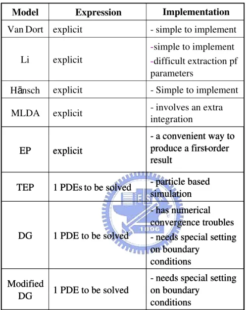
本論文完整介紹隱形式與顯形式的量子修正模式,其中顯形式模式包含
Van Dort’s、Hänsch’s、Li’s、修正的局部密度趨近與有效位勢模式;隱形式模
式分析了密度梯度方程式、修正的密度梯度方程式與熱力學有效位勢模式。論
文中從理論推演以及數值分析方面仔細比較這些模式的優劣之處。量子修正模
式中電子有效質量通常視為可調的數學參數,找出在不同的外加條件下所需要
代入的數值對於半導體工業應用非常有利,尤其是顯形式模式更於容易使用。
在應用上來說,吾人利用量子修正模式研究一維金氧半結構的電容特性以及考
慮二維效應所影響的電流電壓關係式。
總之,本論文已從理論暨數值方向分析不同量子修正方法論的物理模式暨
在金氧半場效電晶體應用之準確性。
ix
Modeling of Quantum Mechanical Effects for Nanoscale MOS Devices with
Correction Theory
Student:Wei-Hsin Chen
Advisors:Dr. Tien-Sheng Chao
Department of Electrophysics National Chiao Tung University
ABSTRACT
By the Moore's Law, chips manufactured on a wafer have approached sub-45 nm regime of gate length for metal-oxide-semiconductor-field-effect-transistors (MOSFETs). Quantum mechanics effects become significant and inevitable. Thus, the transport models used in semiconductors should be corrected by quantum correction models. In this thesis, explicit and implicit quantum correction models are introduced and reviewed completely. There are Van Dort's, Hänsch's, Li’s, modified local density approximation and effective potential models in explicit forms; density-gradient, modified density-gradient, thermodynamic effective potential models are in implicit forms. We compare these models with each other in terms of theoretical and numerical ways respectively. To find the relationship between the effective mass which is treated as fitting parameters in the models with varied physical settings is benefit for industry applications, especially the explicit models, they are simple to be implanted in the simulator. In application, C-V characteristics of a MOS structure and IV curves of a 20 nm double-gate MOSFET are numerically investigated in the work.
xi
誌
謝
本論文得以順利完成,首先要感謝電物系 趙天生教授給予學生最大的自由度,讓學生 得以進行感興趣的研究。學生感謝恩師,電信系 李義明副教授兩年來悉心指導;感謝老 師們於碩士班受業期間對學生論文研究之激勵,思緒慎密之牽引以及觀念之啟迪。感謝李 老師對於學生論文架構之匡正,研究方法傳授及用字遣辭之推敲斟酌。更銘誌於心的是恩 師在為學處世及待人接物之諄諄教誨,使學生在治學方法及處世態度上受益良多,而恩師 在學術研究之嚴謹精神,在半導體元件物理及電腦模擬領域之專業知識與生活處世的積極 與認真的態度,更足以為學生日後之表率。師恩細長,深切銘心,學生在此謹獻上最誠摯 的感謝與敬意。 論文口試期間,承蒙交通大學電子工程系陳明哲教授及交通大學電子物理系陳永富教 授撥冗細審,並惠予寶貴意見與殷切指正使本論文更臻完備。 學生特別感謝台積電前瞻技術部經理楊富量博士給予學生機會,透過李老師與台積電 的研究合作案,讓學生於碩士班二年級時至台積電工讀,學習理論與實務的結合,這難得 的經驗奠定學生對於半導體領域的認識,藉此機會表達對於楊經理富量博士暨台積電的感 謝。 感謝紹銘、正凱、宏穆、傳盛、彥羽、璞學長的照顧幫忙,同窗好友景嵐、柏賢、建 松及婉文的互相砥礪,朝夕相伴,在此一併致謝。 受業期間,承蒙張國明老師、徐琅老師、陳永富老師、謝太炯老師、楊賜麟老師、陳 振芳老師在學業上的悉心指導,在此一併感謝。 學生能順利完成研究所學業,全靠父母、家人及諸位朋友、同學的支持與忍耐,學生 對此由衷感謝。 本 論 文 感 謝 行 政 院 國 家 科 學 委 員 會 ( 計 畫 編 號 NSC-93-2115-E-492-008 、 NSC-94-2115-E-009-084) 、 卓 越 延 續 計 畫 ( 計 畫 編 號 NSC-94-2752-E-009-003-PAE 、 NSC-95-2752-E-009-003-PAE) 、 五 年 五 百 億 計 畫 、 經 濟 部 科 專 計 劃 ( 計 畫 編 號 93-EC-17-A-07-S1-0011)及台灣積體電路製造股份有限公司 2005~2006 年研究計畫之資 助。 謹在此將本論文獻給關心我的人! 陳煒昕 謹誌 中華民國九十五年七月三十一日 于風城交大
Acknowledgments (in English)
I
would like to thank Professor Dr. Tien-Shang Chao of Department of Electrophysicsand Professor Dr. Yiming Li of Department of Communication Engineering in Na-tional Chiao-Tung University. This thesis would not have been possible without their help and support. Professor Chao give me the whole freedom in pursuing this topic. I want to thank Professor Li for the courses I have taken with him and through the many discussions that we have had together.
In addition, I would like to express my appreciation to the members of my examination committee Professor Dr. Ming-Jer Chen and Professor Dr. Yung-Fu Chen for taking the time to read this thesis.
In the second year of my master program, though the project of Prof. Dr. Yiming Li, Man-ager Dr. Fu-Liang Yang gave me a very good opportunity to be an intern at department ETD 2 of TSMC. I am grateful to Manager Dr. Fu-Liang Yang and TSMC for the special experience in exploring semiconductor theory and manufacturing process.
I would also like to thank to all my friends, colleagues, and classmates especially Shao-Ming Yu, Cheng-Kai Chen, Hong-Mu Chou, Chuan-Sheng Wang, Pu Chen, Ching-Lan Chang, Bo-Shian Lee, Chien-Sung Lu and Wan Wen Lo.
I want to thank to the faculty members of National Chiao-Tung University, where I received the education after senior high school. I am lucky to have had the opportunity to learn from so many excellent instructors.
I further wish to acknowledge the financial support by Taiwan National Science Coun-cil (NSC) under constract 93-2115-E-492-008, 94-2752-E-009-003-PAE, NSC-94-2115-E-492-008 and NSC-95-2752-E-009-003-PAE, by the MOE ATU program under a 2006 grant, by the ministry of Economic Affairs, Taiwan, under contract 93-EC-17-A-07-S1-0011 and by the Taiwan Semiconductor Manufacturing Company under a 2004-2006 grant.
Last but not least, I would like to dedicate this thesis to my parents and family for their support and everlasting love and many others where space and time limits further mention of them, who have enriched my life by letting me take a peek through their eyeglass on the world.
Contents
Abstract (in Chinese) . . . v
Abstract (in English) . . . ix
Acknowledgement (in Chinese) . . . xi
Acknowledgments (in English) . . . xiii
List of Tables . . . xviii
List of Figures . . . xix
1 Introduction 1 1.1 Motivation . . . 4
1.2 Literature Review . . . 5
1.3 Outline . . . 7
2 Physical Models in Semiconductor 8 2.1 Maxwell’s Equations . . . 11
xv List of Figures . . . . xvii
xvi CONTENTS
2.2 Classical Transport Models in Semiconductor Device . . . 13
2.2.1 Boltzmann Equation . . . 13
2.2.2 Hydrodynamic Equations . . . 15
2.2.3 Energy Transport Equations . . . 17
2.2.4 Drift-Diffusion Equations . . . 18
2.3 Quantum Approaches in Semiconductor Device . . . 19
2.3.1 Time-independent Schr¨odinger Equation . . . 20
2.3.2 Quantum Transport Theory . . . 27
2.3.3 Quantum Correction Models . . . 29
3 Explicit Quantum Corrections 30 3.1 The Van Dort’s Model . . . 30
3.2 The H¨ansch’s Model . . . 32
3.3 The Li’s Model . . . 34
3.4 The Modified Local Density Approximation Model . . . 35
3.5 The Ferry’s Effective Potential Model . . . 37
4 Implicit Quantum Corrections 40 4.1 The Density-Gradient Model . . . 40
4.2 Thermodynamic Approached Effective Potential Model . . . 44
CONTENTS xvii 4.2.2 Approximations to Thermal Equilibrium . . . 47 4.2.3 Thermodynamic Effective Potential . . . 48 4.2.4 Quantum Barrier Field . . . 57
5 Application to Nanoscale MOS Structures 59
5.1 Effective Mass Calculation for Quantum Correction Models . . . 61 5.2 Computation of Electron Density of MOS Structure under Inversion
Con-dition . . . 67 5.2.1 Single-Gate MOS Structure . . . 67 5.2.2 Double-Gate MOS Structure . . . 70 5.3 Terminal Characteristics Simulation Using Quantum Correction Models . . 75
6 Conclusions 81 6.1 Summary . . . 81 6.2 Future Work . . . 82 References . . . 84 Appendix A VITA . . . 92
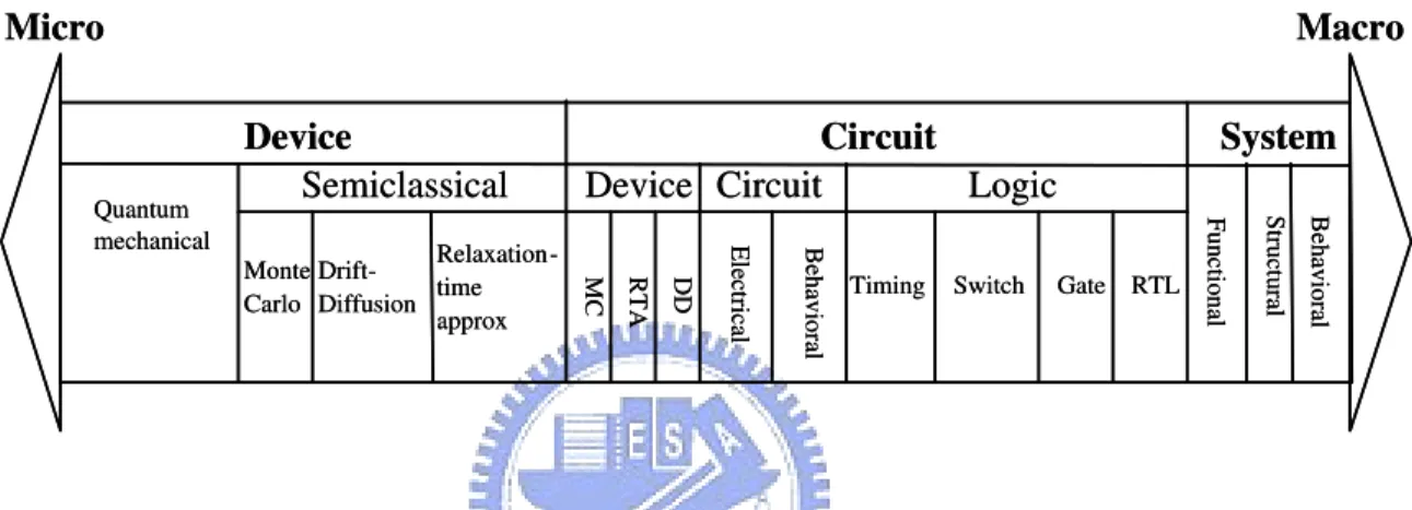
List of Figures
1.1 Hierarchy of semiconductor device simulation. Many small units of device construct together to be a circuit, and then many circuits make a system. . . 3 2.1 A schematic description of the device simulation sequence. The effective
mass of electrons and potential between lattice are calculated. The data is loaded into the transport equation and then the electromagnetic field will upgrade current and charge density until the transport equation and elec-tromagnetic field are solved consistently. After that, density, velocity and temperature of carriers, potential, electric field, I-V curve and C-V curve can be extracted. . . 9 2.2 Illustration of a hierarchy of various transport models.The arrows in the
bottom mean more accurate but costs more time; the upper ones mean more approximate, fast in simulation and easy to implantation. . . 10
xx LIST OF FIGURES
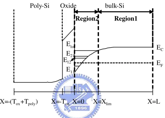
2.3 Single-Gate MOSFET structure. We can draw the band diagram as Fig. 2.4. along the direction of red-dashed cut-line. . . 24 2.4 Energy band diagram of a MOS structure. Toxis oxide thickness, Tpolyis
poly-silicon thickness, Xlim corresponds to the eighth subband and L is the
length od substrate; E11is the first subband, E12is the second subband, E21
is the third subband and Elim is the eighth subband. . . 25
2.5 Schrodinger-Poisson flow chart. Give the initial guesses of potential and electron density first to start the first iteration of self-consistent system. Then the potential from Poisson equation is upgraded, and renew the po-tential term in Schr¨odinger equation simultaneously. If the stop criterion is reached, the self-consistent procedure is done, or the latest potential and electron density have to be upgraded again until the error is small enough [40]. . . 26 4.1 The flow chart of thermodynamic approach. . . 56 5.1 Properties of the quantum correction models for simulation. . . 60 5.2 Single-Gate MOSFET structure, where the red-dashed cut-line is the
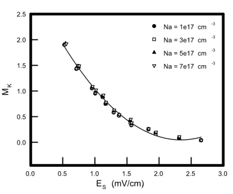
sim-ulation domain. . . 62 5.3 Effective mass, Mk,versus surface electric field, Es, for H¨ansch model by
LIST OF FIGURES xxi 5.4 Effective mass, Mk,versus surface electric field, Es, for MLDA model by
different substrate doping. . . 64 5.5 Effective mass, Mk,versus surface electric field, Es, for EP model by
dif-ferent substrate doping. . . 65 5.6 Effective mass, Mk,versus surface electric field, Es, for DG model by
dif-ferent substrate doping. . . 66 5.7 Comparison of electron density between Schr¨odinger and classical results
for single-gate MOS structure, where gate voltage is 1 V and channel dop-ing is 1e18cm−3 [40]. . . 68
5.8 Comparison of electron density for Schr¨odinger results with verified quan-tum models for single-gate MOS structure, where gate oxide thickness is 1 nm, gate voltage is 1 V and channel doping is 1e18cm−3. ”Sch” means
solutions of Schr¨odinger equation and ”CL” means classical results. . . 69 5.9 Double-gate MOS structure, where the red-dashed cut-line is the
simula-tion domain [21]. . . 71 5.10 Comparison of electron density between Schr¨odinger and classical results
for double-gate MOS structure, where gate oxide thickness is 1 nm, top gate voltage is equal to top gate voltage as 1 V and silicon body thickness is 15 nm [21]. . . 72
xxii LIST OF FIGURES
5.11 Comparison of electron density for Schr¨odinger results with verified quan-tum models for double-gate MOS structure, where gate oxide thickness is 1 nm, top gate voltage is equal to top gate voltage as 1 V and channel doping is 1e17cm−3. . . 73
5.12 Comparison of quantum correction models applied on single-gate and double-gate MOSFETs. . . 74 5.13 Plot of ratio of < x >Sch over < x >EP versus verified gate voltage. The
substrate doping is assumed to be uniform distribution of 1e18cm−3. . . 77
5.14 Comparison of capacitance versus gate voltage between measurement data, Schr¨odinger and effective potential results. . . 78 5.15 2-D electron distribution in a double-gate MOSFET biased at top gate
volt-age is the same as the bottom gate of 1 V and drain voltvolt-age is 0.5 V [21]. . . 79 5.16 Comparison of drain current versus gate voltage calculated by classical and
quantum corrected transport model, where we adopt Li’s model. Top gate voltage is the same as the bottom gate of 0.7 V, gate length is 20 nm, silicon body thickness is 10 nm and gate oxide thickness is 2 nm [21]. . . 80
Chapter 1
Introduction
T
he semiconductor industries have been the major part of today’s technologyde-velopment. With the prediction of Moore’s Law, for the purpose of getting better electrical properties of transistors and a lower costs of very-large-scale integration (VLSI), device scaling is necessary and essential for semiconductor devices in the wafer, especially, metal-oxide-semiconductor field effect transistors (MOSFETs). There are many ways to study electrical characteristics of semiconductor devices. Besides measuring the electrical properties of manufactured chips on wafers in laboratory, there is still another quick and benefit way to analyze semiconductor devices, i.e., simulation and modelling. Simulation of semiconductors is divided into several kinds of ranks, as shown in Fig. 1.1. Many small units of device construct together to be a circuit, and then many circuits make a system. In
2 Chapter 1 : Introduction
this thesis, we concentrate on the device simulation. Simulation with good enough mod-els and computation algorithms will give us precise predictions and trend of the physical features, without tremendous cost of fabrication process and save a lot of time simultane-ously. Cost and time are the two most important issues if the industries can win in present keen competitions. Therefore, device simulation plays an important role in semiconductor industries. By the scaling of a semiconductor device, quantum mechanical effects become significantly influence on the performance of transistors. Thus, models introduced in sim-ulation must consider quantum effects to obtain a correct predictions. Schr¨odinger coupled Poisson’s equations describes the electron behavior as a wave and particle duality and can predict the electrical properties very well compared with experiment data. However, it is time-consuming and difficult to solve in the point of view of numerical methods. Therefore, semi-classical equations with quantum correction models are wildly studied to substitute for Schr¨odinger Equation. The semi-classical models have the most important purposes of speed and accuracy. In the thesis, effective quantum models are studied and compared with each other for nowadays advanced transistors.
This chapter is organized as follows. First of all, the motivation of this work is introduced, then a literature review of quantum correction models in semiconductor device is seated. Finally, outline of the thesis is described in detail.
3
Device Circuit System
Semiclassical Device Circuit Logic
Quantum mechanical Monte Carlo Drift-Diffusion Relaxation-time approx MC RTA DD Electrical Behavioral
Timing Switch Gate RTL
Functional Structural Behavioral
Micro Macro
Device Circuit System
Semiclassical Device Circuit Logic
Quantum mechanical Monte Carlo Drift-Diffusion Relaxation-time approx MC RTA DD Electrical Behavioral
Timing Switch Gate RTL
Functional Structural Behavioral
Micro Macro
Figure 1.1: Hierarchy of semiconductor device simulation. Many small units of device construct together to be a circuit, and then many circuits make a system.
4 Chapter 1 : Introduction
1.1 Motivation
With the continuous scaling down of the semiconductor devices. For example, gate ox-ide thickness less than 1 nanometer (nm) results in a large electric field in the interface between oxide and silicon and make the quantum well deep and narrow. The energy of electron wave functions in the inversion layer are quantized and limit the transport of elec-trons from source to drain. Therefore, the classical transport and other physical models are not accurate enough to obtain correct simulation results. Replacing the classical models by quantum ones are indispensable to consider the quantum effects, which are significant in today’s nanoscale semiconductor devices. Nevertheless, it takes much time for a general computer in a lab when dealing with full quantum model, for example, the Schr¨odinger equation, and therefore loses the benefit of fast speed. Simulation with classical models but importing an effective quantum term to approximate fully considered quantum models can keep the merits of fast and accuracy. However, the approximations of quantum effect proposed previously will lead to results which are not accurate enough or introduce some mathematical parameters which have no physical meanings. How to choose between ac-curacy and speed when using quantum correction models is what we concern about. In the thesis, we compare these quantum correction models in the point of view of theory and numerical simulation.
1.2 : Literature Review 5
1.2 Literature Review
The importance of quantum effects in inversion layers of MOSFETs was recognized in the late 1950s by Schrieffer [1]. The initial research of quantum mechanical confinement in inversion layers was by Stern and Howard [2]. Later, Stern calculated energy levels, charge distribution, and electrostatic potential self-consistently in inverted p-type semiconductors [3]. Since the oxide thickness is continually reduced in order to maintain good control of the gate in nano-scale channel length regime, quantum mechanics become more signifi-cant. And a number of additional theoretical studies have been undertaken, such as Van Dort’s model [4], the density-gradient approach [5], the modified local density approxima-tion method, and the effective potential method [6]-[10]. Specifically, in the late 1980’s, Hansch studies carrier transport at the interface between gate oxide and semiconductor, then developed a formula that allows an approximate incorporation of quantum mechani-cal boundary effects on the carrier distribution [11]. In the early 1990’s, Van Dort used a simple method to model the silicon bandgap under the inversion condition [4]. He treated the quantum effects associated with the confinement of minority carriers in the inversion layer [12]. Although his model can predict the capacitance for a wide range of different doping levels, it fails to describe the quantum effect on the spatial distribution of elec-trons near the boundary layer, i.e. the pick value of electron distribution will away from the interface od Si/SiO2. The density-gradient method is another approximation quantum
6 Chapter 1 : Introduction
treatment.It is a macroscopic approach to the quantum confinement problem. In the early 1980’s, M. G. Ancona and H. F. Tiersten generalized the equation of describing the elec-tron gas state to include density-gradient dependence [13]-[15]. Later it was extended to characterize the quantum- mechanical behavior of electrons distributed in strong inversion layers. Recently, Ancona and coworkers made further progress on this physically based approach and pointed out that the density-gradient approximation is an effective tool for engineering-oriented analysis of electronic devices in which quantum confinement and tun-nelling phenomena are obvious [16]. The modified local density approximation (MLDA) approach was first used by Paasch and H. Ubensee in 1982 [17]. Using this method, they studied the electron density in an inversion layer in the semiconductor-insulator interface, which is approached with a triangular potential. Recently, an IBM semiconductor device simulation group developed a computationally efficient algorithm based on the MLDA. This model predicts the spatial distribution of the quantized carriers which the previously proposed simple models failed to do so. In the recent years, a effective potential (EP) ap-proach has been proposed, which has the advantages of easy numerical implementation and almost guaranteed convergence [18][19]. The effective conduction-band edge equa-tion which wants to improve the problem for density-gradient equaequa-tion of a differential of a high order electron density is introduced [20]. In 2003, an improved Van Dort model is proposed, which is more to the results of Schr¨odinger-Poisson Equations. However, the
1.3 : Outline 7 fitting parameters have to be extracted by the optimization theory [21]. And then, a ther-modynamic effective potential removes the disadvantage that fitting parameter has to be modified in different physical setting in Ferry’s effective potential theory. Alternatively, the size of an electron is decided by its energy [22].
1.3 Outline
Physical models in semiconductor are shown in Chap. 2 and then basic descriptions of ex-plicit and imex-plicit quantum mechanical approximation models in Chap. 3 and Chap. 4, the new quantum potential correction models are investigated there. In Chap. 5, the application and comparison for MOS Structures by quantum correction models are displayed. Chap. 6 includes a summary of this work and suggestion for possible future work.
Chapter 2
Physical Models in Semiconductor
T
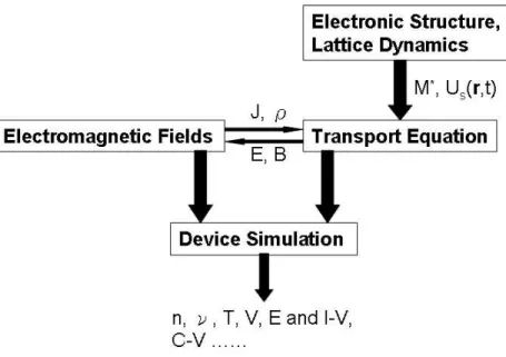
he electrical properties in semiconductor devices are the most important factorswhen judging if they are suitable for the applications, for example, high frequency or microwave devices. The main concepts of semiconductor device simulation have two components [23], which must be solved self-consistently with each other, i.e. the transport equations governing charge flow and the fields driving charge flow, as shown in Fig. 2.1. We can calculate the effective mass of electrons and potential between lattice. The data is loaded into the transport equation and then the electromagnetic field will upgrade current and charge density until the transport equation and electromagnetic field are solved con-sistently. After that, density, velocity and temperature of carriers, potential, electric field, I-V curve and C-V curve can be extracted [23]. To include the quantum mechanics, the
9
Figure 2.1: A schematic description of the device simulation sequence. The effective mass of electrons and potential between lattice are calculated. The data is loaded into the transport equation and then the electromagnetic field will upgrade current and charge density until the transport equation and electromagnetic field are solved consistently. After that, density, velocity and temperature of carriers, potential, electric field, I-V curve and C-V curve can be extracted.
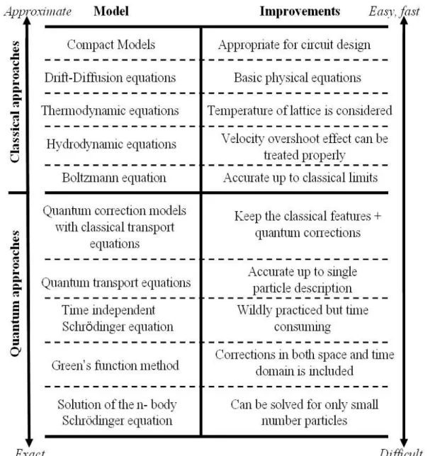
direct solution of many-body time-dependant Schr¨odinger equations are only suitable for few number of particles, so it’s not a possible way to be used in semiconductor. Alterna-tively, approximation methods are often adopted for simulation, as shown in Fig. 2.2. The arrows in the bottom mean more accurate but costs more time; the upper ones mean more approximate, fast and easy. The selection of models depends on the compromise between accuracy and speed. These models are described in detail in the next sections.
10 Chapter 2 : Physical Models in Semiconductor
Figure 2.2: Illustration of a hierarchy of various transport models.The arrows in the bottom mean more accurate but costs more time; the upper ones mean more approximate, fast in simulation and easy to implantation.
2.1 : Maxwell’s Equations 11
2.1 Maxwell’s Equations
The fields for the charge and current density are obtained from solving Maxwell’s equations [24][25] ∇ × ~H = ~J + ∂ ~D ∂t, (2.1) ∇ × ~E = −∂ ~∂tB, (2.2) ∇ · ~D = ρ, (2.3) and ∇ · ~B = 0, (2.4)
where ~E and ~Dare the electric field and displacement vector. ~H and ~B are the magnetic field and induction vector. ~J denotes the conduction current density and ρ is the electric charge density. Under appropriate conditions [26], only the quasi-static electric fields aris-ing from the solutions of Poisson’s equation are necessary. Poisson’s equation is essentially derived from ∇ · ~D = ρ. By substituted for some basic physical formulas, given by
~
D = ε · ~E, (2.5)
~
12 Chapter 2 : Physical Models in Semiconductor
and
ρ = q(p − n + NA+− N −
D), (2.7)
where ε is the permittivity tensor and V is the potential. q denotes the electron charge. p, n, N+
A and N −
D are densities of hole, electron, ionized acceptors and ionized donors,
respectively. Then a Poisson’s equation has the form of ∇ · V = q ε(n − p + N − D − N + A). (2.8)
The continuity equation can be derived from Maxwell’s equation or Boltzmann equation. In this section, deviation form ∇ × ~H = ~J + ∂ ~∂tD by ~J = ~Jp + ~Jn with assumptions of
unchanged donors and acceptors with respect to time is shown as ∇ · ( ~Jp+ ~Jn) + q ·
∂
∂t(p − n) = 0. (2.9)
Considering the generation and recombination term, R, and then Eq. (2.9) becomes ∇ · ( ~Jn) − q · ∂n ∂t = q · R, (2.10) and ∇ · ( ~Jp) + q · ∂p ∂t = −q · R, (2.11)
2.2 : Classical Transport Models in Semiconductor Device 13
2.2 Classical Transport Models in Semiconductor Device
In the numerical analysis, the current are characterized by either classical or quantum trans-port equations. Before the gate lengths of MOSFETs are scaled down to less than 100 nm by the rule of Moore’s Law [27], the transport properties is sufficient to be described by classical transport equations. Semiconductor equations, derived from the Boltzmann trans-port equation, are the basis of the majority of current device models, where the dimensions of the device geometry are greater than a de Broglie wavelength of electrons. The classical transport equations are introduced in the next sections.
The transport equation used in semiconductor in classical regime is based on Boltzmann equation and its simplified models, i.e. hydrodynamic, thermodynamic and drift-diffusion models.
2.2.1 Boltzmann Equation
The Boltzmann transport equation describes the temporal evolution of the single-particle distribution function f(r, p, t) in the phase space [28]. The coordinates of particles in space, r, and momentum, p, at a certain time can be characterized well. Assume there are scattering effects , the distribution function is given by [28]
df (r, p, t)
dt =
∂f
14 Chapter 2 : Physical Models in Semiconductor
which expands to yield [26], ∂f ∂t + ∂r ∂t · ∇rf + ∂p ∂t · ∇pf = ∂f ∂tcollision. (2.13)
The rate of change of momentum ∂~p
∂t is equal to the applied force F = q ~E(~r, t) and ∂~r ∂t is
equal to the group velocity, ~u(~k). ~p is substituted by ~k~. Then Eq. (2.12) can be written as ∂f (~r, ~k, t) ∂t + ~u(k) · ∇rf (~r, ~k, t) + −q ~E(~r, t) ~ · ∇kf (~r, ~k, t) = ∂f~r, ~k, t ∂t collision. (2.14)
In Boltzmann equation, carriers are treated as classical particles which are uncorrelated with position ~r and momentum ~k at time t. A many-particle system of carriers and be ex-pressed as single-particle distribution [29].
The Boltzmann euqation is the most accurate in the classical limit and a statistical Monte Carlo method is used to find the distribution function. However, it consumes the compu-tation a lot. Therefore, some simplified equations, for example, hydrodynamic equations, are adopted to replace Boltzmann equation for the purpose of compromise between accu-racy and simulation time. Before preforming the deviation, some equations are defined as follows, n(~r, t) is the electron concentration:
n(~r, t) = Z ∞
−∞
f (~r, ~k, t)d~k; (2.15)
vdn(~r, t)is the electron average velocity;
n(~r, t)vdn((~r, t)) =
Z ∞
−∞
2.2 : Classical Transport Models in Semiconductor Device 15 ωn(~r, t)is the electron average energy:
n(~r, t)ωn((~r, t)) = m∗ n 2 Z ∞ −∞|~u(~k)| 2f (~r, ~k, t)d~k; (2.17) ~
Tn(~r, t)is the electron temperature tensor:
1 2n(~r, t)kBT~n((~r, t)) = m∗ n 2 Z ∞ −∞ [~u(~k) − vdn(~r, t)]f (~r, ~k, t)d~k; and (2.18) ~
Qn(~r, t)is the heat flow vector:
~ Qn((~r, t)) = m∗ n 2 Z ∞ −∞[~u(~k) − v dn(~r, t)]|~u(~k) − vdn(~r, t)|2f (~r, ~k, t)d~k. (2.19)
2.2.2 Hydrodynamic Equations
If we multiply a χ(~k) in Eq. (2.14) and integrate from minus infinity to infinity, Eq. (2.14) becomes [30] Z ∞ −∞ χ(~k)∂f (~r, ~k, t) ∂t d~k + Z ∞ −∞ χ(~k)~u(k)· ∇rf (~r, ~k, t)d~k + Z ∞ −∞ χ(~k)−q ~E(~r, t)~ ·∇kf (~r, ~k, t)d~k = Z ∞ −∞ χ(~k)∂f~r, ~k, t ∂t collisiond~k. (2.20)
Then balance equations are decided through assumptions [30][31]. If χ(~k) is defined as 1, i.e. the 0th order approximation, then Eq. (2.20) is derived to the carrier balance equation,
16 Chapter 2 : Physical Models in Semiconductor
given by
∂n(~r, t)
∂t + ∇r(n(~r, t)~vdn(~r, t)) = G(~r, t) − R(~r, t). (2.21) If χ(~k) is defined as m∗
n~u(~k), i.e. the 1st order approximation, then Eq. (2.20) is derived to
the momentum balance equation, given by ∂(n(~r, t)~vdn(~r, t)) ∂t + ∇r· n(~r, t)kBT~n(~r, t) m∗ n + ∇ r· (n(~r, t)~vdn(~r, t)2) + q ~E m∗ n n(~r, t) = ∂(n(~r, t)vdn(~r, t)) ∂t collision. (2.22) If χ(~k) is defined as1 2m ∗
n~u(~k)2, i.e. the 2nd order approximation, then Eq. (2.20) is derived
to the energy balance equation, given by ∂(n(~r, t)~ωn(~r, t))
∂t + ∇r· [~vdn(~r, t)n(~r, t)ωn(~r, t) + ~vdn(~r, t) · n(~r, t)kBT~n(~r, t) + ~Qn(~r, t)] + qn(~r, t)~vdn(~r, t) · ~E =
∂(n(~r, t)~ωn(~r, t))
∂t collision. (2.23)
The hydrodynamic equations for electron is composed by these three parts shown above. Therefore, we need to solve seven partial differential equations for using the hydrodynamic model when considering electron, hole, and Poisson equations. The model can reproduce hot carrier effects as velocity overshoot and accurate impact ionization generation rates which drift-diffusion model lacks [32].
2.2 : Classical Transport Models in Semiconductor Device 17
2.2.3 Energy Transport Equations
The energy transport equations only consider particle conservation, Eq. (2.21), and en-ergy conservation, Eq. (2.23) [33], which lacks momentum conservation compared with hydrodynamic model. It accounts for electrothermal effects, under the assumption that charge carriers are in thermal equilibrium with the lattice [34]. Under approximations [35], particle conservation relation becomes:
∂n ∂t =
1
q∇ · ~Jn− R, (2.24)
where ~Jnis the electron current density, shown as
~
Jn = −qµnn∇φ + qDn∇n + µnkBn∇Tn. (2.25)
Energy balance equation becomes: ∂(nωn)
∂t = −∇ · ~Sn+ ~Jn· ~E − n
ωn− ω0
τnω(Tn)
, (2.26)
where ~Snis the electron energy flux, shown as
~ Sn = ~ Jn −qωn+ ~ Jn −qkBTn+ ~Qn. (2.27)
ωnis the average carrier energy and ~Qnis the heat flux, given by
ωn = 3 2kBTn+ 1 2m ∗ nv2dn, (2.28) and ~ Qn = −2Tn( kB q ) 2nqµ n∇Tn. (2.29)
18 Chapter 2 : Physical Models in Semiconductor
Therefore, including electron, hole and Poisson equations, we have to solve five partial differential equations when considering energy transport equations.
2.2.4 Drift-Diffusion Equations
The drift-diffusion equations are widely used for the simulation of carrier transport in semi-conductors by its simple and fast properties in simulation [36]. It should be considered carefully because some properties such as heat effects, are neglected in the model. We only use the carrier balance equation, Eq. (2.21), to have, for electron [36],
∂n ∂t = 1 q∇ · ~Jn− R, (2.30) where ~ Jn = −qµnn∇φ + qDn∇n. (2.31)
Accordingly, only three partial differential equations need to be solved when considering electron, hole and Poisson’s equations.
2.3 : Quantum Approaches in Semiconductor Device 19
2.3 Quantum Approaches in Semiconductor Device
The sizes of MOSFETs fabricated on silicon substrate for VLSI have been scaled in order to attain better performance and higher integration. The gate length of a MOSFET (multi-gates) keeps shrinking even over 10 nm [37]. With the size reduction of the horizontal direction, i.e. direction from source to drain, the vertical direction such as gate oxide thick-ness and depletion layer thickthick-ness scale down at the same time to lead to a strong quantum confinement effects [38].
Accordingly, two significant quantum effects appear, for example, a shift in the threshold voltage due to a rise of the lowest occupied subband above the minimum conduction band energy and a reduction in the gate capacitance because of the setback of the maximum in the inverted electron density away from Si/SiO2 interface. These quantized effects can be
integrated into the classical models though some kinds of quantum approximation which has explicit or implicit forms. However, if the lateral quantization becomes important, then a full quantum mechanical model is required to deal with the device. In this section, a brief description for quantum approximations is given.
20 Chapter 2 : Physical Models in Semiconductor
2.3.1 Time-independent Schr¨odinger Equation
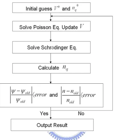
The direct solution of many-body Schr¨odinger equation can be solved only for small num-ber of particles, so it’s not possible to be applied into the whole device simulation. Thus, we approximate the quantum effects into single-state and time-independent Schr¨odinger Equa-tion and then coupled with the Poisson equaEqua-tion. Classical transport models are adopted when current calculation is needed. We consider a MOS structure, where the metal part is replaced by polycrystal silicon with a p-type silicon as substrate. Two assumptions are adopted [39]. The first, Fermi-Dirac distribution is employed and the second, stan-dard electron and hole effective-mass approximations in a parabolic shaped band are as-sumed. Fig. 2.4 shows the energy band diagram of a MOS structure. The flow chart of the self-consistent Schr¨odinger and Poisson system is shown in Fig. 2.5 [40]. We must first give the initial guesses of potential and electron density to start the first iteration of self-consistent system. We can get a upgraded potential from Poisson equation, Eq. (2.8), and renew the potential term in Schr¨odinger equation simultaneously. The nest step is to solve Schr¨odinger equation, which is shown below,
− ~
2
2mxk
d2
dx2ζjk(x) + EC(x)ζjk(x) = Ejkζjk(x), (2.32)
where mxkis the effective mass normal to the interface in the kth valley, Ejk is the energy
levels of the jth subband in the kth valley, and ζjk is the wave function of the jth subband
2.3 : Quantum Approaches in Semiconductor Device 21 boundary. Because the silicon crystal has a six-folds ellipse-shape band energy diagram, there are two different effective mass (mjk) when dealing with different kth valley. It should
be chosen carefully.
After the Schr¨odinger equation is solved, wave function and eigen-energy are known. And then charge density can be calculated.
Region 1, i.e. the silicon bulk region, where the electron energy is continuous and therefore all energy levels above the conduction band minimum edge (EC) are permissible. Electron
density in the classical region is calculated by [41]
ncl = Nceγ[1 − c1eγ+ c2e2γ]. (2.33) where, γ(x) = EF − EC(x) kBT = EF − (−qψ(x)) kBT , c1 = 0.3536, and c2 = 0.1290.
And electrons in the inversion region near the surface of Si/SiO2in silicon substrate (region
2) are treated as a two dimensional electron gas (2DEG) with a splitting of energy levels into subbands. Where the electrons are divided into two parts: (1) One of them is calculated as 2DEG where the potential is sufficiently narrow to quantize the motion in the inversion
22 Chapter 2 : Physical Models in Semiconductor
layer, and (2) the others whose energies are above Elim behave like classical particles. As
shown below,
n = nq+ ncl. (2.34)
If the first eight subbands are considered, nq is given by [42]
nq(x) = kBT π~2 2 X k=1 gkmdk X j ln[ 1 + exp( EF−Ejk kBT ) 1 + exp(EF−Elim kBT ) ]|ζjk|2. (2.35)
where, ζjkis the envelope function of the jth subband in the kth valley, gkis the degeneracy
factor of the kth valley, and mdk is the parallel effective mass in the kth valley. And the
electrons behave classically as ncl(x) = NC 2 √π Z ∞ ξ0(x) √ ξdξ 1 + exp ξ − γ(x), (2.36) where, ξ0(x) = Elim− (−qψ(x)) kBT .
The hole has no quantum confinement and the density p can be calculated by the classical Boltzmann distribution,
p = NV exp(
EV(x) − EF
κBT
). (2.37)
Therefore, the charge density in the inversion layer is calculated by ρ = q(p − n + ND+− N
−
A). (2.38)
We get the new ncl and nq. If the system has not converge, the charge density term in
2.3 : Quantum Approaches in Semiconductor Device 23 carries on until convergence criterion is achieved. The total inversion layer charge < Q > is obtained by the integration over electron density, which is defined as
< Q >= Z
0
n(r)dr, (2.39)
where n(r) is electron density. The average inversion charge depth < X > is defined as < X >= R 0rn(r)dr R 0n(r)dr . (2.40)
The Schr¨odinger-Poisson system is the most accurate way of steady-state to treat the quan-tum confinement problems in the inversion layer at the Si/SiO2 interface. But it has the
fatal disadvantages of taking too much time and consuming the computer efficiency seri-ously when dealing with the eigen-value problems of Schr¨odinger equations. However, the quantum effect is a very important phenomenon that can’t be neglected in such small scale dimension of transistors. Therefore, not only for the applications of industries but also for the research of academics, the quantum approximation models (quantum correction mod-els) are developed for the purpose of replacing the Schr¨odinger equations by approximation of mathematical forms to get a much fast simulation speed and accurate enough results in the past years. In brief, these models have the explicit and implicit types and are summa-rized in the next chapters.
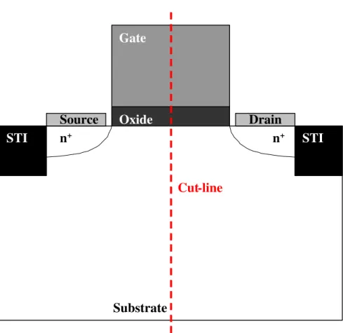
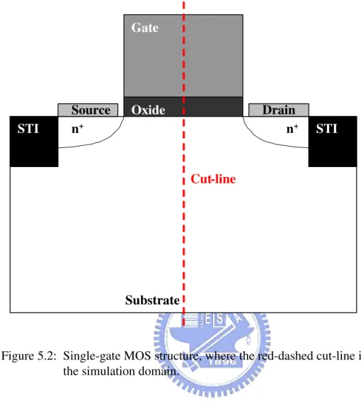
24 Chapter 2 : Physical Models in Semiconductor Gate Oxide Substrate Cut-line STI STI Source Drain n+ n+
Figure 2.3: Single-gate MOS structure. We can draw the band diagram as Fig. 2.4. along the direction of red-dashed cut-line.
2.3 : Quantum Approaches in Semiconductor Device 25
Poly-Si
Oxide
bulk-Si
E
CE
FE
limE
E
1221E
11Region1
Region2
X=L
X=X
limX=0
X=-T
oxX=-(T
ox+T
poly)
Figure 2.4: Energy band diagram of a MOS structure. Toxis oxide
thickness, Tpolyis poly-silicon thickness, Xlimcorresponds
to the eighth subband and L is the length od substrate; E11is
the first subband, E12is the second subband, E21is the third
26 Chapter 2 : Physical Models in Semiconductor
Figure 2.5: Schrodinger-Poisson flow chart. Give the initial guesses of potential and electron density first to start the first iteration of self-consistent system. Then the potential from Poisson equation is upgraded, and renew the potential term in Schr¨odinger equation simultaneously. If the stop criterion is reached, the self-consistent procedure is done, or the latest potential and electron density have to be upgraded again until the error is small enough [40].
2.3 : Quantum Approaches in Semiconductor Device 27
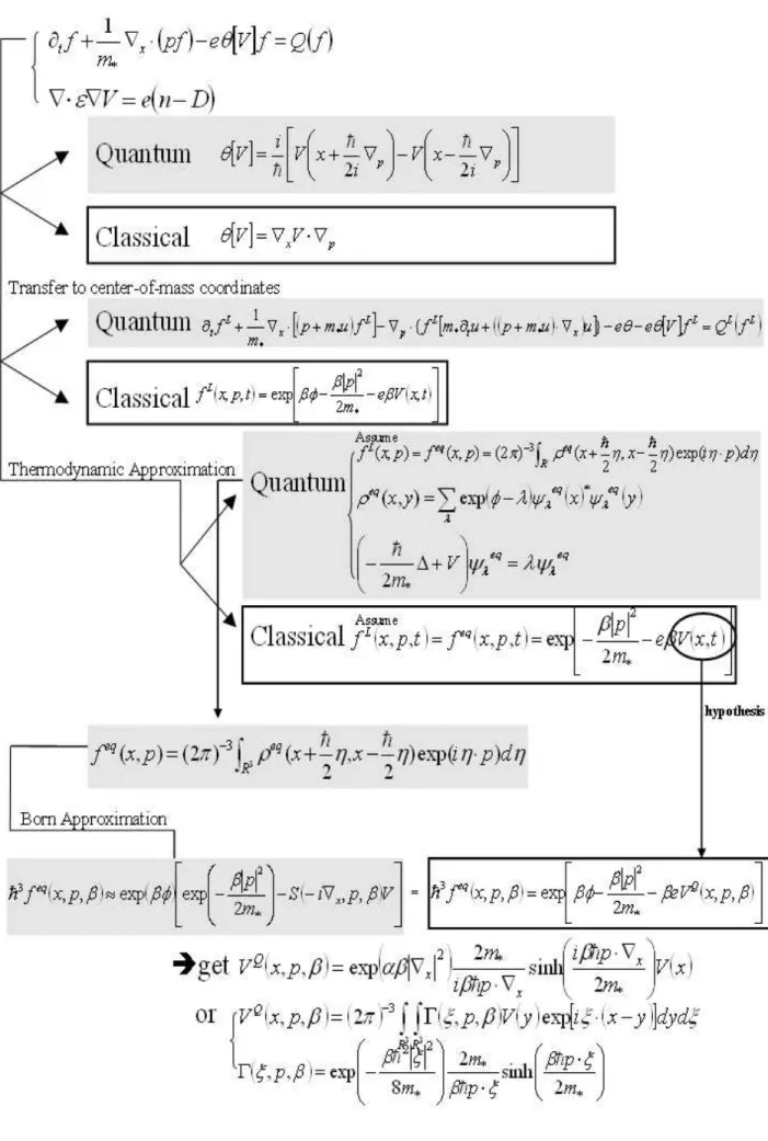
2.3.2 Quantum Transport Theory
If a system containing a large number of particles is not completely known, we usually use the statistical physics of concept of statistical ensemble. Classical transport physics is based on the concept of probability distribution function which describe the phase space of carriers. However, in quantum mechanics, obtaining details about position and momentum simultaneously contradicts the Heisenberg’s Uncertainty Principle. Therefore, it is given by a probability density matrix in terms of quantum mechanics. The rate of change of the probability density matrix ρ with time is determined by Lioville-von Neumann equation, given by [43][26]
i~∂ρ
∂t = [H, ρ], (2.41)
where the density matrix, ρ, is defined as ρ =
∞
X
i=0
ρi|ψiihψi|. (2.42)
This is the quantum analogue of the Liouville equation in classical transport equation, shown as ∂ρ ∂t = {H, ρ}, ⇒ ∂ρ∂t = n X i=1 (∂H ∂qi ∂ρ ∂pi − ∂ρ ∂qi ∂H ∂pi ) (2.43)
There is another alternative approach. Draw an analogy to classical concept of a phase-space distribution function, the quantum mechanics use a Wigner distribution function. It
28 Chapter 2 : Physical Models in Semiconductor
is very similar to Boltzmann equation with the constraints of the uncertainty principle but has no simple interpretation in the concept of probability theory since it is not definitely positive definite. Wigner function extends the concept of distribution to the quantum case and it constitutes the more direct link between the quantum density matrix and the classical description of the evolution of the system in phase space though a distribution function f (~r, ~p, t), defined by [22] f (~r, ~p, t) = (2π)−3Z R3 ρ(~r + ~ 2η, ~r − ~ 2η)exp(iη · ~p)dη. (2.44) By analogy with Boltzmann transport equation, the Wigner transport equation has a similar form, given by ∂tf + 1 m∗∇r· (~pf) − eθ[V ]f = ( ∂f ∂t)collision, (2.45) where θ[V ] is a pseudodifferentail operator, shown as
θ[V ] = ~i[V (~r + ~
2i∇p) − V (~r − ~
2i∇p)]. (2.46)
And the action of θ[V ] is given by θ[V ]f (~r, ~p, t) = (2π)−3Z R3 Z R3 i ~[V (~r + ~ 2η) − V (~r − ~ 2η)]f (~r, ~q, t)exp[iη · (~p − ~q)]dqdη. (2.47) Quantum transport theory is used to explain and support confidence limits for the classical Boltzmann transport theory.
2.3 : Quantum Approaches in Semiconductor Device 29
2.3.3 Quantum Correction Models
Without solving Schr¨odinger equation and using the quantum transport theory, there is an-other way to consider quantum mechanical effects into device simulation. It is a semiclas-sical method to treat the quantum effects by replacing a classemiclas-sical potential by a corrected potential or a classical carrier concentration by corrected carrier one. This kind of quantum correction methods are not as accuracy as what has been discussed in the previous sections, they are compromises between precision and calculating time. Fast speed in simulation is the most beneficial in semiclassical transport equations with quantum correction models. It is easy to upgrade the potential or carrier concentration term in classical transport equations and there are two types of such quantum correction models, i.e. explicit and implicit mod-els. They are introduced by detail in Chap. 3 and Chap. 4. In the commercial simulation tools, drift-diffusion transport equations with quantum corrected models are wildly adopted because of properties of simple and fast. Similarly, the hydrodynamic and Boltzmann equa-tions can also transformed to semiclassical form by renewing the correction term. Which sort of transport models is chosen just depends on what physical phenomenons need to be considered in simulation process.
Chapter 3
Explicit Quantum Corrections
I
n the chapter, the explicit quantum corrections, i.e., the Van Dort’s model, H¨anschmodel, Li’s model, MLDA model and effective potential model, are discussed in terms of theoretical viewpoint.
3.1 The Van Dort’s Model
The Van Dort’s model considers the quantum effect at the interface of Si/SiO2as a effective
rise of the minimum conduction band edge as a widened bandgap. The model proposes that the quantum corrected surface potential ψQ
s is larger than the conventional potential ψsconv
by [4]
ψQs = ψsconv+∆E
q + εs∆¯x, (3.1)
3.1 : The Van Dort’s Model 31 where ∆E is the energy level difference between the minimum conduction band edge and the first allowed energy level E11in the quantized region at the interface, εs is the surface
electric field, and ∆¯x is the difference of the average displacement of electrons from inter-face of Si/SiO2 between classical and quantum solutions. If the bandgap is larger enough,
we can approximate the quantum corrected intrinsic carrier concentration nQ
i , which is shown as nQi = niexp( EF − E Q g 2 kBT ) = niexp( EF − E2g kBT )exp(4E1 2kBT ) = nconvi exp(E Q g − Egconv 2kBT ), (3.2) where nconv
i is the classical model for the intrinsic carrier concentration, EgQ is quantum
corrected bandgap, and Econv
g is the original bandgap. E1 is the difference between EgQand
Econv
g . Since the quantum effect is only significant near the interface, a weighting factor
W (x)can be introduced approximately as
W (x) = 2 exp(−a
2)
1 + exp(−2a2), (3.3)
to model the potential distribution in the direction perpendicular to the interface of Si/SiO2.
Where a = x
xref and xref is a reference distance (xref
≈25 nm). Thus, the upgraded and quantum corrected intrinsic carrier concentration niis given by
ni = nconvi [1 − W (x)] + W (x)n Q
32 Chapter 3 : Explicit Quantum Corrections
Although the Van Dort’s Model has a simple mathematical form to implement to the classi-cal solver, it has the drawbacks that it is not accurate because of triangular well approxima-tion and it cannot predict the condiapproxima-tion that the peak electron density value has a distance away from the Si/SiO2 interface. The electron density will still has the largest value at
the interface like the behavior of classical electrons. The method can only describe the decreasing electron density accounting for a reduced effective bandgap.
3.2 The H¨ansch’s Model
The H¨ansch’s Model approximates the electron concentration density with quantum cor-rection as [11] nQ(x) = N Cexp(−qψ(x) − qφF kBT )[1 − exp(− x2 λ2 th )], (3.5)
where λth is the thermal wavelength shown as
λth = s ~2 2m∗ nkBT , mk = m∗ n 9.11 × 10⁻³¹ kg. (3.6)
λthis a measure of how fast the quantum effect decreases away from the interface, m∗nis an
3.2 : The H¨ansch’s Model 33 and EF is fermi level. This model is smoothed to have a classical electron density when
the position is far away from the interface of Si/SiO2, shown as
nclassical(x) = NCexp(−qψ(x) − qφF
kBT
). (3.7)
It is a classical model of electron density which is corrected by an additional term, 1 − exp(−x2
λ2
th). The electron concentration changes rapidly in the boundary layer (Si/SiO2
interface), it is difficult to evaluate an accurate value from Poisson equation. Generally, we can assume the electron concentration is proportional to (x − xinterf ace)2 at interface
and this assumption is valid for electron concentration for H¨ansch’s, modified local density approximation and density gradient approximation models, it can be written as
nQ = const. × (x − xinterf ace)2. (3.8)
Therefore, some assumptions are exhibited as follows. The sheet charge density Ns in the
boundary has the form of Ns = Z 12dx1 0 (p(x) − n(x) + N + D(x) − N − A(x))dx, (3.9)
where dx1 = x1 − x0, which means the difference between first and second mesh in
nu-merical simulation and N+
D(x) − N −
A(x) ≈ −NA(x). p(x) and NA(x)are the hole density
and substrate doping concentration, respectively, which can be treated as constants equal to p0 and NA0 in the dx1. If dx1 λth, Eq. 3.9 becomes
Ns= (p0 − NA0) 1 2dx1+ Z 12dx1 0 n(x)dx. (3.10)
34 Chapter 3 : Explicit Quantum Corrections
The potential within dx1 is regarded as constant because dx1 is very small. By these
ap-proximations, nQin the boundary is proportional to x2, given by
nQbounary = NCexp(− qφF − qψ kBT ) · ( x2 λ2 th ). (3.11)
And Eq. (3.7) can be modified by Fermi-Dirac statics, shown as nQ(x) = NCF1/2(− qφF − qψ(x) kBT )[1 − exp(− x2 λ2 th )]. (3.12)
The H¨ansch’s model has more physical meanings than Van Dort’s model described above, but it has the shortcoming that the adjustable mathematical parameter mkis very sensitive
by different cases, for example, different substrate doping, gate oxide thickness and applied gate voltage may all need exclusive mkto have accurate enough results compared with the
Schr¨odinger-Poisson self-consistent ones. It is not so convenient for real applications but may be treated as the initial guesses for other quantum correction models which are dis-cussed as follows.
3.3 The Li’s Model
This model [21] improves H¨ansch’s model to have a more accurate electron distribution and the peak value of electron. It has a very close results compared with Schr¨odinfer-Poisson’s. However, the difficulty is how to extract three parameters shown below. In the paper [21],
3.4 : The Modified Local Density Approximation Model 35 they are extracted by the optimization theory. The model is shown as
nQ(x) = a0nCL(x) · (1 − exp[−a1ξ2(1 − 1 2( ξ ξ0 )2) − a2ξ3]), (3.13)
where nCL(x)is the classical electron density solved with the Poisson equation, ξ = x/λth
and λthis the thermal wavelength. For the double-gate case, ξ0 = Tsi/2λth, where Tsiis the
thickness of silicon body. a0, a1 and a2 are optimized and calibrated with the
Schr¨odinger-Poisson solutions by optimization theory.
3.4 The Modified Local Density Approximation Model
Paasch and Ubensee firstly proposed a quantum correction model called modified local den-sity approximation model which is applicable even if there is a abrupt variance in potential [17]. In the case of interface of Si/SiO2, the quantum corrected electron density is
approx-imated by adding an additional correction term into the classical model in an integration form, given by nQ(x) = NC 2 √ π Z ∞ 0 dξ · ξ0.5 1 + exp(ξ − k(x)) − NC 2 √π Z ∞ 0 dξ · ξ0.5 1 + exp(ξ − k(x))Σ 6 i=1j0 (2x√ξ/λi n) 6 = NC 2 √ π Z ∞ 0 dξ · ξ0.5 1 + exp(ξ − k(x))[1 − Σ 6 i=1j0 (2x√ξ/λi n) 6 ], (3.14)
36 Chapter 3 : Explicit Quantum Corrections where, ξ = E − Ec) kBT , k(x) = EF + qψ(x) kBT , and λin = s ~2 2mi∗ nkBT . (3.15)
xis the distance counted from the interface, NC is conduction band effective
density-of-state, j0 is the zeroth-order spherical Bessel function, EF is fermi level, and λth is the
thermal wavelength as described above.
The effective mass is usually considered to take an average value between longitudinal and transverse ones because the six-fold ellipse-shape symmetry of valleys when calculating the spherical Bessel function j0. Note that the model smooths the curve behavior between
quantum and classical regimes. For region which is far from the Si/SiO2 interface, Eq.
(3.14) becomes n(x) = NC 2 √ π Z ∞ 0 dξ · ξ0.5 1 + exp(ξ − k(x)). (3.16)
At x = 0, Eq. (3.16) gives n(x) = 0, which is consistent with the assumption that wave function vanishes at the boundary. The thermal wavelength λth is a characteristic
length which depends on the temperature and the effective mass m∗
ncan been seem to be
a adjustable parameter to fit Schr¨odinger-Poisson solutions. MLDA model is much more efficient to solve a numerical integration than a Schr¨odinger-Poisson solver which need to solve an eignevalue problem. Besides, the fitting parameter mk is less sensitive than
3.5 : The Ferry’s Effective Potential Model 37 H¨ansch model. It is the advantage when implanted into the device simulators.
3.5 The Ferry’s Effective Potential Model
In analogy to the smoothed potential representations for the quantum hydrodynamic model (density-gradient model), David K. Ferry suggested an effective potential model that emerges from the wave packet description of particle motion, where the extent of the wave packet spread is obtained from the range of wave vectors in the thermal distribution function [18][19]. This form for the effective potential allows one to build in certain quantum ef-fects that arise from the non-zero size of the electron wave packet. It can be derived from potential part of the Hamiltonian, given by
Hv =
Z
drV (r)n(r). (3.17)
Using the wavepacket description leads to Hv = Z drV (r)X i ni(r) (3.18) = Z drV (r)X i Z dr0exp(−|r − r 0 |2 a2 )δ(r 0 − ri) = X i Z drδ(r0 − ri) Z dr0 V (r0 )exp(−|r − r 0 |2 a2 ).
The primed integration is defined as effective potential, VQ, and the finite size of the
38 Chapter 3 : Explicit Quantum Corrections
as
VQ(x) = Z
V (x + ξ)G(ξ, a0)dξ, (3.19)
where G is a Gaussian with the standard deviation a0. a0 is defined as a0 = ~/√8m∗kBT.
In three dimensions, it becomes
VQ(x, y, z) = 1 (2π)1.5a xayaz Z Z Z V (x0 , y0 , z0 ) exp(−(x − x 0 )2 2a2 x − (y − y 0 )2 2a2 y − (z − z 0 )2 2a2 z )dx0 dy0 dz0 , (3.20) where V (x0 , y0 , z0
)is the classical potential and ax,y,zare the standard deviations of Gaussian
integration. This model is easy to integrate into the classical models. The effective poten-tial VQ is related to the self-consistent potential obtained from Poisson equation. We just
need to perform an integral-smoothing transformation to original potential with gaussian function. We can expand Eq. (3.19) in Taylor series. The one-dimensional case becomes
VQ(x) = √ 1 2πa0 Z ∞ −∞V (x + ξ)exp(− ξ2 2a2 0 )dξ ∼ = √ 1 2πa0 Z ∞ −∞ [V (x) + ξ∂V ∂x + ξ2 2 ∂2V ∂x2 + · · · ]exp(− ξ2 2a2 0 )dξ. = V (x) + a20∂ 2V ∂x2 + · · · . (3.21)
In nondegenerate semiconductors, V can be described by (ln n
n0)/(−β), Eq. (3.21) be-comes VQ(x) = V (x) − 2a 2 0 β ∂2ln(pn/n 0) ∂x2 + · · · (3.22) = V (x) − 2a 2 0 β√n ∂2√n ∂x2 + · · · .
3.5 : The Ferry’s Effective Potential Model 39 Therefore, Ferry’s effective potential is related to the relation of gradient of density term, which is usually known as Bohm potential. Although the effective potential model has the advantage that it is a convenient way to produce a first-order result, drawbacks such as solution is overestimated and peak location is further setback from the material interfaces are inevitable.
Chapter 4
Implicit Quantum Corrections
I
n the chapter, the implicit quantum corrections, i.e. The density-gradient model,ef-fective conduction band edge model and thermodynamic approximation model, are discussed in terms of theoretical viewpoint.
4.1 The Density-Gradient Model
The quantum potential originates from hydrodynamic formulation of quantum mechanics by Bohm and is developed by Ancona is called density-gradient model [13]-[15]. Begin from the one-particle Schr¨odinger equation, of the form
i~∂ψ ∂t = − ~2 2m∇ 2ψ + V (x)ψ. (4.1) 40
4.1 : The Density-Gradient Model 41 The wave function is written in complex form in terms of its amplitude R(r, t) and phase S(r, t)as
ψ(r, t) = R(r, t) exp(iS(r, t)~ ). (4.2)
Then substituted back into the Schr¨odinger equation, one arrives at the following coupled equations for the density and phase given as
∂R(r, t) ∂t = − 1 2m[R(r, t)∇ 2 S(r, t) + 2∇R(r, t) · ∇S(r, t)], (4.3) and ∂S(r, t) ∂t = −[ [∇S(r, t)]2 2m + V (r, t) − ~2 2m ∇2R(r, t) R(r, t) ]. (4.4)
We can write ρ(r, t) = R(r, t)2, where ρ(r, t) is the probability density and obtain
∂ρ(r, t) ∂t + ∇ · [ρ(r, t) 1 m∇S(r, t)] = 0, (4.5) and −∂S(r, t)∂t = [∇S(r, t)] 2 2m + V (r, t) + V Q. (4.6)
In the classical limit, the above equation are subject to a very simple interpretation. The function S(r, t) is a solution of the Hamiltonian-Jacobi equation. If we consider an ensem-ble of particle trajectories which are solutions of the equations of motion, if all these tra-jectories are normal to any given surface of constant S, then they are normal to all sureface of constant S. And ∇S(r,t)
m means the velocity vector. Eq. 4.5 can be written as
∂ρ(r, t)
42 Chapter 4 : Implicit Quantum Corrections
Since ρ(r, t) is the probability density, ρv isthe mean current of particles in this ensemble, and Eq. (4.7) expresses continuity equation. Eq. (4.5) and Eq. (4.6) have the form of clas-sical hydrodynamic equations with a additional potential, often referred to as the quantum potential (Bohm potential) [44], shown as
VQ = − ~ 2 2mR∇ 2R = − ~2 2m√n ∂2√n ∂x2 , (4.8)
where the density n is related to the probability density as n(r, t) = Nρ(r, t) = NR(r, t)2,
N is the total number of particles in the ensemble. Nevertheless, an extra term is intro-duced in the carrier flux by making the equation of state for the electron desity-gradient dependance. The current density is corrected as
− → Jn= −qnµn∇ψ + qDn∇n − qnµn∇(2bn∇ 2√n √ n ), (4.9)
where bnis the density-gradient coefficient which determines the strength of the gradient
effect in the electron gas. The last term in the right hand side of Eq. (4.9) is referred to as ”quantum diffusion”, which makes the electron continuity equation has a fourth-order partial differential equation. Therefore, such an approach is highly sensitive to noise in the local carrier density, and the methodology is highly important in cases of strong quantization. However, advantages of not so sensitive parameter bn compared with other
quantum approximation models and results close to Schr¨odinger-Poisson solutions make the density-gradient model is commonly used in commercial semiconductor simulators for
4.1 : The Density-Gradient Model 43 quantum correction.
The gradient equation may be simplified to a simpler form, say modified density-gradient equation. We note that a similar idea has been proposed [20]. Eq. (4.8) can be represented by V∗ (r) = Vcl(r) − VQ(r), = Vcl(r) − ~ 2 2mr ∇2√n √ n , = Vcl(r) − ~2 4mr[∇ 2lnn(r) + 1 2(∇lnn(r)) 2], (4.10) where V∗
is the effective total potential energy and Vcl is the classical potential. r is
chosen between 1 and 3. For obtaining the effective conduction-band edge equation, we propose that in the equilibrium Boltzmann distribution, after quantum correction, lnn(r) is proportional to −V∗
(r)/kBT and not to −V (r)/kBT. Thus, Eq. (4.10) becomes
V∗ (r) = Vcl(r) + ~ 2 4mrkBT[∇ 2V∗ (r) − 1 2kBT(∇V ∗ (r))2]. (4.11)
The effective conduction-band edge equation has the improvement that no serious request for a very well defined mesh, as used in general density-gradient equation because the high-order differential of carrier density is replaced by effective total potential energy.
44 Chapter 4 : Implicit Quantum Corrections
4.2 Thermodynamic Approached Effective Potential Model
There is an alternative to the approach outlined above. The mean idea of a thermodynamic approached effective potential model is essentially a perturbation theory around thermal equilibrium [22][45]. We seek a semiclassical transport equation with a quantum corrected potential whose classical commutator, [εef f, f ]
classicalwill produce the same thermal
equi-librium state as Wigner commutator [ε, f]W, where f is a distribution function evaluated
from Weyl quantization [46]. The process is detailed in the next sections.
4.2.1 Classical and Quantum Collisionless Boltzmann Equations
We start from transforming the many-body Schr¨odinger-Poisson system to a analog of the collisionless Boltzmann-Poisson equations which assumes mean field theories and effective mass approximations for ensemble by use of Wigner transformation, given by [46][47]f (x, p, t) = (2π)−3 Z R3 ρ(x + ~ 2η, x − ~ 2η)exp(iη · p)dη, (4.12) where ρ(x, y, t) = ΣλF (λ)ψλ(x)∗ψλ(y). (4.13)
4.2 : Thermodynamic Approached Effective Potential Model 45 ρ(x, y, t)means the density matrix of mixed state and ψλis wave function with eigen energy
λ. The Wigner function satisfies the Wigner, or collisionless quantum Boltzmann equation ∂tf + [ε, f ]W = 0, ε = |p| 2 2m∗ + eV (x, t) ⇒ ∂tf + i ~ X υ=±1 υε(x + iυ~ 2 ∇p, p − iυ~ 2 ∇x)f = 0 and ⇒ ∂tf + 1 m∗∇x· (pf) − ie ~[V (x + ~ 2i∇p) − V (x − ~ 2i∇p)] = 0, (4.14) which can be taken as a pseudodifferentail operators θ[V ] by
∂tf + 1 m∗∇x· (pf) − eθ[V ]f = 0, (4.15) where θ[V ] = ~i[V (x + ~ 2i∇p) − V (x − ~ 2i∇p)]. (4.16)
And the action of θ[V ] is given by
θ[V ]f (x, p, t) = (2π)−3Z R3 Z R3 i ~[V (x + ~ 2η) − V (x − ~ 2η)] · f(x, q, t)exp[iη · (p − q)]dqdη. (4.17)
In the effective potential approach, one replaces the quantum Boltzmann equation by a cor-responding semiclassical equation with a modified potential. Thus, Wigner commutator
46 Chapter 4 : Implicit Quantum Corrections
[ε, f ]W is replaced by the classical commutator [εef f, f ]classical, the semiclassical
Boltz-mann equation is given by
∂tf + [εef f, f ]classical = 0, ε = |p| 2 2m∗ + eV ef f(x, t), ⇒ ∂tf + ∇pεef f · ∇xf − ∇xεef f · ∇pf = 0, and ⇒ ∂tf + 1 m∗∇x· (pf) − e∇p· (∇xV ef ff ) = 0. (4.18)
Therefore, all quantum effects are taken into account by the force acting on the elec-tron. The quantum corrections through the semiclassical transport equations are Wigner-Boltzmann-Poisson system shown below,
∂tf + 1 m∗∇x· (pf) − eθ[V ]f = Q(f), ∇ · ε∇V = e(n − D), n(x, t) = Z R3 f (x, p, t)dp, (4.19)
where Q(f) denotes the collision operator when considering collision process and it’s zero when modelling collisionless one. e denotes the electron charge, D is the doping concen-tration and n(x, t) means the density of electrons.
4.2 : Thermodynamic Approached Effective Potential Model 47
4.2.2 Approximations to Thermal Equilibrium
The effective potential is based on the perturbation theory around thermal equilibrium. We want to find a semiclassical transport equation with a quantum corrected potential whose classical commutator, [εef f, f ]
classical will produce the same thermal equilibrium state as
Wigner commutator [ε, f]W when applying to a quantum system. Our purpose is to make
the two operators shown above equal to each other and then extract the effective potential to be used in semiclassical transport equations [22].
First, starting from the Wigner-Boltzmann-Poisson system, Eq. (4.19) and transform it to center-of-mass coordinates. The mean velocity u(x,t) of the ensemble is defined as
Z R3 pf (x, p, t)dp = m∗ un(x, t), n(x, t) = Z R3 f (x, p, t)dp, (4.20) and then choose m∗
u to be the origin of the center-of-mass coordinates in momentum space. Make the Lagrangian transformation to Wigner equation, shown as [22]
∂tfL+ 1 m∗∇x·[(p+m ∗ u)fL]−∇p·fL[m ∗ ∂tu + ((p + m ∗ u) · ∇x)u]−eθ[V ]fL = QL(fL), (4.21) where fL(x, p, t) = f (x, p + m∗ u(x, t), t)and QL(fL)(x, p, t) = Q(f )(x, p + m∗u, t).
The thermal equilibrium in classical case have the form of feq = ~−3exp(−βεef f),
⇒ fL(x, p, t) ≈ feq(x, p, t) = exp[−β|p|
2
2m∗ − βeV
48 Chapter 4 : Implicit Quantum Corrections
On the other hand, in the quantum mechanics, the thermal equilibrium state is defined as a density matrix as [48][49]
ρeq = exp(−βH), (4.23)
where H is the Hamiltonian operator and β is 1/kBT. Taking use of the definition of
Wigner function, i.e. Weyl quantization, feq(x, p, t) = (2π)−3Z R3 ρeq(x + ~ 2η, x − ~ 2η)exp(iη · p)dη, ρeq(x, y) =X λ exp[β(φ − λ)]ψλeq(x) ∗ ψeqλ (y), (− ~ 2 2m∗∆ + eV )ψ eq λ = λψ eq λ . (4.24)
Therefore, the effective potential can be derived approximately from substituting exp(−βεef f)
for Weyl quantization of exp(−βH) [50]. Now we already have a description for classi-cal case in thermal equilibrium, and then the next step is to get an analyticlassi-cal solution of quantum state of thermal equilibrium. The procedure is shown in the following section.
4.2.3 Thermodynamic Effective Potential
We need to find a explicit expression in quantum distribution function in thermal equi-librium, feq, in order to get a formula of effective potential Vef f. Of course, it is not