國立交通大學
顯示科技研究所
碩士論文
矽光伏特材料於低溫薄膜電晶體之應用
Application of photovoltaic silicon materials in low temperature
thin film transistor
碩士生:詹皇彥
指導教授:黃中垚 教授
謝嘉民 教授
矽光伏特材料於低溫薄膜電晶體之應用
Application of photovoltaic silicon materials in low
temperature thin film transistor
研究生:詹皇彥
Student: Huang-Yan Jhan
指導教授:黃中垚
Advisor: Jung Y. Huang
謝嘉民 Jia-Min Shieh
國立交通大學
顯示科技研究所
碩士論文
A Thesis
Submitted to the Display Institute
Collage of Electrical Engineering and Computer Science National Chiao Tung University
in Partial Fulfillment of the Requirements for the Degree of Master
in
Electro-Optical Engineering July 2010
Hsinchu, Taiwan
i
矽光伏特材料於低溫薄膜電晶體之應用
學生:詹皇彥
指導教授:黃中垚
謝嘉民
國立交通大學顯示科技研究所碩士班
摘要
大面積軟性電路展現新型態的電子裝置,快速的崛起在顯示、感應裝置、生醫 及其他領域。除此之外軟性電子元件更具備許多優點,輕量化、可饒式、耐用、可 以因應更多自由的設計。因為氫化非晶矽薄膜電晶體的成熟的低溫製程,現階段是 最常被使用在液晶顯示器以及軟性電子,然而最大的缺點便是較低的電子遷移率、 不穩定性以及較高的驅動電壓。近來研究發展顯示奈米或稱微晶矽的材料是具有取 代氫化非晶矽成為新一代軟性電子及大面積電子元件潛力 本篇論文中,利用高密度電漿化學氣相沉積系統及熱燈絲化學氣相沉積系統在 低溫 200o C 下沉積出高結晶性的氫化微晶矽薄膜以及低電阻率的 n 型氫化微晶矽薄 膜,並且藉由 XRD 及 SEM 確認氫化微晶矽薄膜,確認晶粒大小約 100nm 等同於一 般非晶矽藉由固相結晶法(Solid Phase Crystallization) 600℃退火 24 小時的結晶性。使 用簡單的自我對準式薄膜電晶體,藉由場效傳導法(Field Effect Conductance)取出缺陷 密度(Density of states)從中了解不同結晶度對於缺陷密度分布之影響。最後將低缺陷 密度之氫化微晶矽及 n 型氫化微晶矽薄膜整合成功的製作出不需離子佈植、低成本、低溫、高結晶性的薄膜電晶體,開與關的電流差距超過 105
、開關速度達到 S=100 mV/decade,並且電子遷移率達到50 cm2/V-s 展現出極高的潛力應用於軟性電子元件。
ii
Application of photovoltaic silicon materials in low
temperature thin film transistor
Student: Huang-Yan Jhan
Advisor:Dr.Jung Y. Huang
Dr.Jia-Min Shieh
Display Institute
National Chiao Tung University
Abstract
Flexible, large area circuits exhibit a new form of electronics which have
led to rapidly rising and promising applications in displays, sensors, medical
devices and other areas. Besides flexible electronics on plastic substrates
possess advantageous characteristics, being lightweight, flexible, and have the
capacity to be manufactured in a variety of shapes, which leads to freedom of
design. Currently, a-Si:H TFTs are used in AMLCD and compatible with
flexible substrate due to low temperature process. However,
low device
mobility, higher drive voltage and electrical instability are the main
disadvantages of a-Si TFT. Recent developments reveal that micro- or
nanocrystalline silicon is a promising alternative for flexible display and large
area electronic applications. The charge carrier mobility exceeds the mobility
of amorphous silicon significantly and compatible with flexible substrate.
In this thesis, a high quality and low resistivity of intrinsic and n-type
microcrystalline silicon films were developed at low temperature 200
oC by
High Density Plasma chemical vapor deposition system and Hot-Wire
chemical vapor deposition system. First μc-Si:H film was analyzed by XRD
and SEM. And the μc-Si:H with a grain sizes of ~50-100 nm was recognized.
iii
The grain size is the same with conventional SPC(600℃ annealing 24hours)
method. A self-aligned TFTs was demonstrated. After that, the density of state
distribution was extracted from TFTs by FEC method. With these results we
can understand the different crystallinity on the effect of defect density
distribution. Finally a top-gate microcrystalline TFTs without S/D
implantation was demonstrated. A high electron mobility exceeding 50
cm
2/V-s, low subthreshold swing 0.1-0.3 V/decade and high current ON/OFF
ratios more than 10
5was obtained. It shows highly potential in flexible
electronics application.
iv
誌謝
本論文能夠順利完成,首先要感謝我的指導老師黃中垚教授及謝嘉民教授,使 我在兩年的研究所學習生涯中,得以培養出獨立研究的能力。特別感謝國家奈米元 件實驗室謝嘉民博士給予我細心的指導與鼓勵,讓我知道實驗的方向及效率是影響 成果優劣的最重要因素。其次,也要謝謝郭浩中教授及沈昌宏博士及戴寶通博士擔 任我的口試委員,提供我不少的寶貴意見。 感謝奈米元件實驗室工程師游文謙、王昭凱、黃文賢大哥們以及彥佑、耿正在 實驗上對我的指導及實驗儀器上的幫助,你們的經驗與指教幫助我度過不少難關。 感謝博士班學長們,宥浦學長在機台以及材料上提供許多的寶貴經驗與意見、建華 學長的機台使用經驗、小閩學長、尚融學長的討論與指教,你們的指點幫忙讓我的 研究更加順利。感謝和我共同奮鬥的同學們:泓瑜、育新、智維、國欽、舒純真的很 慶幸能遇見你們這群可愛的朋友,有你們的陪伴,兩年的生活更加多采多姿。也謝 謝所有學弟妹默默地付出,使我能順利的完成研究。祝福你們未來的實驗順利。 最後,謹將本論文獻給我的父母。謝謝他們辛苦的支持與不斷的鼓勵,使我 能順利完成學位。v
Contents
摘要
... i
Abstract ... ii
誌謝
... iv
Contents ... v
List of figures ... vi
Chapter 1 Introduction ... 1
1.1 The general background and motivation ... 1
1.2 TFT Structures ... 3
Chapter 2 Material Characterization ... 5
2.1 Introduction of amorphous and microcrystalline silicon ... 5
2.2 Growth mechanisms of microcrystalline silicon thin films ... 7
2.3 Electronic properties of amorphous silicon (a-Si:H) and microcrystalline silicon (uc-Si:H) ... 9
2.4 Density of states extraction using FEC method ... 11
Chapter 3 Experimental Details ... 14
3.1 Measurement system setup ... 14
3.2 Capacitance fabrication ... 15
3.3 Laser-activatied amorphous silicon (a-Si:H) and microcrystalline silicon (uc-Si:H) self-aligned TFTs ... 15
3.4 In-situ dopant microcrystalline silicon TFTs ... 18
Chapter 4 Results and Discussions ... 21
4.1 CV measurement ... 21
4.2 Microcrystalline silicon film characterization ... 24
4.3 Highly conductive doped flim ... 29
4.4 IV characterization and Density of states of laser-activated self-aligned TFTs ... 31
vi
Chapter 5 Conclusions and Future work ... 44
5.1 Conclusions ... 44
5.2 Future work ... 44
Reference ... 45
List of figures
Fig. 1 Schematic of commonly used TFT structures ... 4Fig. 2 Microstructure of microcrystalline silicon as a function of the crystalline volume fraction. ... 7
Fig. 3 The standard model for density of states in a-Si:H. ... 10
Fig. 4 Schematic diagram of C-V measurement system. ... 14
Fig. 5Laser activated self-aligned TFTs fabrication flow chart ... 17
Fig. 6In-situ dopant TFTs fabrication flow chart ... 20
Fig. 7 Schematic of metal-oxide-semiconductor (MOS) structure and top vie ... 21
Fig. 8 (a),(b)and (c) Typical capacitance-voltage (C-V) characteristic of MOS capacitors were fabricated with ICP power as 200W,250W and 300W respectively ... 23
Fig. 9 (a),(b) shows the XRD spectra of μc-Si:H by HDPCVD and HWCVD ... 26
Fig. 10 (a)TEM image of μc-Si:H by HDPCVD (b) Incubation layer of 20nm ... 27
Fig. 11 (a), (b) Plane-view SEM images of intrinsic and n-type μc-Si:H (c) The cross-section of μc-SiH i-layer films structure by HWCVD ... 28
Fig. 12 Schematic of metal-semiconductor device ... 29
Fig. 13 (a) IV-curve of Intrinsic nc-Si;H film (b) Resistivity of n+nc-Si:H with different PH3 dopant ... 30
Fig. 14 Schematic cross section of self-aligned amorphous/microcrystalline silicon TFT. ... 34 Fig. 15 (a) Transfer and (b) output characteristics of amorphous silicon n-type TFTs by
vii
HDP-CVD ... 35 Fig. 16 (a) Transfer and (b) output characteristics of microcrystalline silicon n-type TFTs by HDP-CVD ... 36 Fig. 17 (a) Transfer and (b) output characteristics of microcrystalline silicon n-type TFTs by HW-CVD ... 37 Fig. 18 The density of states distribution of amorphous/microcrystalline TFTs were
extracted from Field Effect Conductance (FEC) method. ... 38 Fig. 19 Schematic cross-section of a standard n-channel top-gate staggered ... 40 Fig. 20 (a) Transfer and (b) output characteristics of amorphous silicon n-type TFTs by
HDP-CVD ... 41 Fig. 21(a) Transfer and (b) output characteristics of amorphous silicon n-type TFTs by
HWP-CVD ... 42 Fig. 22 The density of states distribution of in-situ doped TFTs were extracted from Field Effect Conductance (FEC) method. ... 43 Fig. 23 (a) ,(b)shows schematic three-dimensional of in-situ doped TFTs and top view 43
1
Chapter 1 Introduction
1.1 The general background and motivation
Thin-film transistors (TFT), which use a thin semiconductor film on an insulating substrate as the active channel, was first demonstrated in 1961 by Dr. P. K. Weimer. However the first TFT used CdSe as the active device channel, not now commonly used amorphous Si(a-Si). Until 1979 the first amorphous Si TFT was demonstrated by P. G. le Comber , W. E. Spear. With its simplicity in structure and fabrication, applications of thin-film transistors in image sensors and displays become more and more popular. But for now the great demand information and desire high resolution displays has stimulated higher interest in poly-Si TFT. This is due to a much higher mobility and drive current of poly-Si TFTs, compared to amorphous Si counterparts, which enables the integration of peripheral circuits on the same panel in active matrix liquid crystal displays (AMLCD) manufacturing [1][2].
Generally, AMLCDs used a-Si TFTs as a switching element to control the gray level in liquid crystal display(LCD) [5] In AMLCDs, TFTs play as switching device to turn ON/OFF the current path for charging/discharging the liquid crystal capacitor. However, a-Si TFTs has poor effect field mobility (0.5-1 cm2/V-s) and higher turned on voltage. In order to improve the TFTs performance, the poly-Si TFT was developed in 1980 by S.W. Depp and A. Juliana. The undoped poly-Si was deposited by low-pressure CVD at 625 OC, and the films were approximately 0.75 m thick.[3] The major advantage of polycrystalline silicon poly-Si TFT technology is its suitability for multifunctional active-matrix displays, because it enables the integration of driver electronics, sensors, memories, and peripheral circuits on the glass substrate to produce system-on-glass SOG displays. But the temperature in the
2
process is too high to use on glass. Therefore in 1991 T.W. Little and K. Takahara developed low-temperature (T≦600 oC) polycrystalline silicon thin film transistor (poly-Si TFTs) which was fabricated by solid phase crystallization (SPC) of amorphous silicon(a-Si).[4]
Over the years, amorphous, polycrystalline, and recently, nano/microcrystalline forms of silicon have gained prominence as low temperature alternatives to crystalline silicon for large-area applications. Amorphous silicon is the current material for most of the thin film transistors used in liquid crystal displays, and a host of other applications. It is a versatile material for limited mobility applications, and can be reliably grown at very low temperatures, but suffers from bias stress and light induced degradation. Polycrystalline silicon on the other hand has much higher mobilities, and hence suitable for high-speed CMOS applications. But it requires processing at much higher temperatures, which is out of scope of inexpensive plastic substrates. Although methods of converting amorphous silicon to polycrystalline silicon exist by laser induced crystallization, it suffers from problems of device uniformity besides being expensive.
For this reason we have been pursuing thin-film transistor technology based on nano/microcrystalline silicon, nc-Si:H/μc-Si:H as an inexpensive alternative. This semiconductor can provide sufficient electron mobility [5–7].Moreover, it can be fabricated at low temperatures which are compatible with the plastic substrates [7]. The table 1. summarizes the low-temperature silicon processes prevalent at present. Although amorphous silicon-based TFTs are currently used in addressing the pixels of AMLCD. The material is deposited at low temperature compatible with the use of plastics. However, the low field effect mobility in these TFTs limits the panel size.[8] Then, TFTs with higher mobility are needed. Nano/Microcrystalline silicon (nc-Si) is now the main candidate to reach this goal.It can be deposited by different techniques
3
at low temperature compatible with the use of plastics substrates. In this thesis, a-Si:H TFTs and nc-Si:H/μc-Si:H TFTs were demonstrated under low temperature(T≦200
oC) by HWCVD and HDPCVD.
Table 1. Status of silicon materials for TFTs [10]
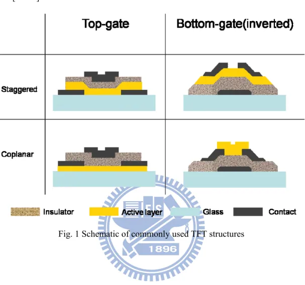
1.2 TFT Structures
The thin-film transistor usually refers to MOSFET as opposed to other kinds of transistors. The structure is similar to MOSFET. It can be roughly classified into top-gate and bottom-gate types depending upon the placement of the gate dielectric relative to the channel material. In bottom-gate (inverted) devices, the gate dielectric is below the active layer, while in top-gate devices the gate dielectric layer is above the active layer similar to conventional MOSFETS. These can be further classified into coplanar and staggered types depending upon the location of the source and drain contacts relative to the gate. In coplanar TFTs, the source and drain contacts are on the same side of the active region as the gate contact, whereas in staggered structures, the source and drain contacts are on the opposite side of the active region as compared to the gate contact. These device geometries are schematically described in the Fig. 1. The inverted staggered in currently industry is most commonly used structure for a-Si:H TFT. One of the most important reasons for this is that silicon nitride forms an excellent gate dielectric with amorphous silicon which is currently the material of choice owing to low cost and low temperature fabrication. In this thesis a top-gate
4
structure was used to take advantage of the highly crystalline top surface of the film.[11-14].
5
Chapter 2 Material Characterization
2.1 Introduction of amorphous and microcrystalline silicon
In crystalline silicon, the silicon atoms are covalently bonded with four neighbors in tetrahedral directions. The bond of bonding states (valance band) is completely occupied with electrons, and the antibonding bond (conduction band) is empty. Electrons can cross the energy gap by thermal or optical excitation. Impurity introduced states within the gap, such as boron or phosphorous, govern the electronic properties.
In amorphous silicon the conduction and valance bands have tails of states due to fluctuations of the bond lengths and bond angles in the silicon matrix. These states are modified band states. They can be divided into localized and extended states. Charge carriers in localized states have near zero mobility. Extended states provide a finite mobility to carriers, and they are separated from localized states by a conceptual mobility edge, which defines a mobility gap. In brief, the amorphous semiconductors are noncrystalline, and they lack long-range periodic ordering of their constituent atoms. But they do have a local order on the atomic scale. This short-range order is directly responsible for observable semiconductor properties such as optical absorption edges and activated electrical conductivities.
Polycrystalline semiconductors are composed of grains, with each grain containing a periodic array of atoms surrounded by a layer of interconnective or boundary atoms. For progressively smaller grains, such as microcrystallites, the surface layer of each grain contains progressively larger numbers of interconnective randomly distributed atoms relative to the periodically arrayed interior atoms. Consequently, a semiconductor containing a larger number of very small grains
6
embedded in the amorphous phase of the material is called the microcrystalline (or noncrystalline) semiconductor. The microcrystalline semiconductors lie on the borderline between the amorphous and polycrystalline phases, and the difference between polycrystalline and microcrystalline semiconductors is the content of the amorphous phase. The relative amount of crystalline phase contained in the film is described by the crystalline volume fraction, which can vary from a few percent up to 80 or 90% in fully crystallized samples. In general, in polycrystalline semiconductors, the content of the amorphous phase is negligible and is mainly located at the grain boundaries, and in microcrystalline semiconductors the content of the amorphous phase is variable. If the volume fraction of the amorphous phase is not negligible, the device electronic properties can still be dominated by the amorphous phase [1].
7
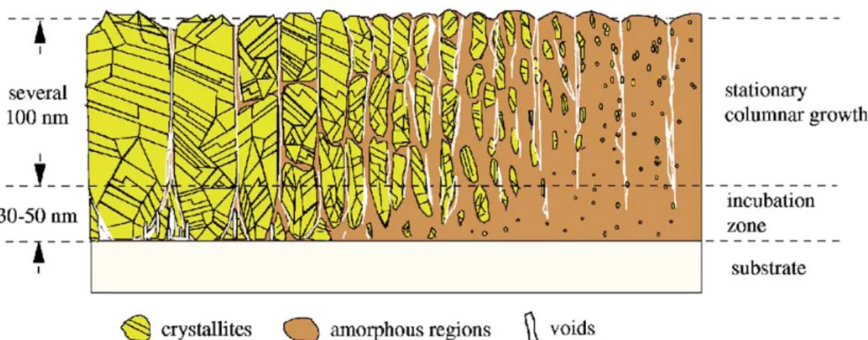
2.2 Growth mechanisms of microcrystalline silicon thin films
Microcrystalline silicon μc-Si:H consists of silicon crystallites, amorphous phases, and voids.[2] The microstructure of microcrystalline silicon can be controlled from highly crystalline to a material where amorphous growth prevails Fig. 2[3] It is well known that high hydrogen (H2) dilution in a silane (SiH4) plasma can induce
a microstructural change from amorphous to ordered structures even at low temperatures,300 °C,[4],[5] This behavior can be also observed in Hot-wire chemical-vapor deposition system.[6] There are three primary model to understand the formation of uc-Si:H films at low temperatures (100-350 ℃ ) for PECVD.
Fig. 2 Microstructure of microcrystalline silicon as a function of the crystalline volume fraction.
І. Surface diffusion model:
This model was proposal to explain the relationship between crystalline volume fraction in the resulting uc-Si:H films and substrate temperature during growth of the films. Sufficient flux density of atomic hydrogen from hydrogen diluted silane plasma realizes a full surface coverage by bonded hydrogen and also produces local heating through hydrogen-recombination reactions on the growth surface of the film. These two events occurring on the surface enhance the surface diffusion length of film
8
precursor (SiH3). As a consequence, film precursors adsorbed on the surface can find energetically stable sites, leading to a formation of atomically flat surface. At first, uc nucleus is formed. After the formation of nucleus, epitaxial like crystal growth takes place with a similarly enhanced diffusion of film precursors [7, 8].
ІІ. Etching model:
This model was proposed based on the experimental fact that film growth rate is reduced by an increase of hydrogen dilution. An atomic hydrogen provided on the film-growing surface breaks Si-Si bonds, preferentially the weak bond, involved in the amorphous network structure, leading to a removal of a Si atom bonded more weakly to another Si. This site is replaced by a new film precursor, forming a rigid and strong Si-Si bond [9, 10].
ІІІ. Chemical annealing model:
The model was proposed for explaining the experimental fact that crystalline formation is observed during hydrogen plasma treatment in a layer-by layer growth by an alternating sequence of amorphous film growth and hydrogen plasma treatment. During the hydrogen plasma treatment, many hydrogen atoms are permeating in the sub-surface region, giving rise to a crystallization of amorphous network through the formation of a flexible network with a sufficient amount of atomic hydrogen in the sub-surface region without any removal process of Si atoms [11].
9
2.3 Electronic properties of amorphous silicon (a-Si:H) and
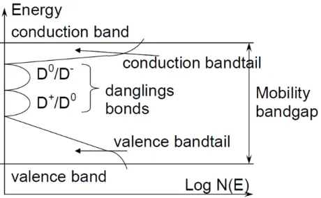
microcrystalline silicon (uc-Si:H)
The electronic properties of the amorphous silicon(a-Si:H) and microcrystalline silicon (uc-Si:H) depend sensitively on the density and energy distribution N(E) of the localized gap states. And these states determine the doping efficiency, transport, and recombination, as well as the width and the potential profile of space charge layers in devices. Fig. 3 shows a model of this density of states distribution including both intrinsic and extrinsic defect states. Tails of localized states extend from both bands deep into the gap. And these states are believed to arise from potential fluctuation due to the disorder. In addition to these tail states, one excepts to discover states in the gap from specific defects. Such defects will be formed in random network structure in order to release internal tension, but they may also arise from unfavorable deposition conditions. The simplest intrinsic defect is an unsaturated bond-the so-called “dangling” bond-the neutral state of which is located around midgap in undoped material; however, in principle, there can also be more complicated defects that act as deep centers. Both the concentration and energy distribution of these states are determined by the position of the Fermi level. In undoped a-Si:H, the concentration of these defects can be as lower as 1015cm-3. Due to the low density of gap states, the Fermi level in such films can easily be moved by doping, illumination, or external bias to a space charge layer.
10
11
2.4 Density of states extraction using FEC method
As mentioned in section 2.3 , the electronic properties is strongly affected by density and energy distribution N(E) of the localized gap states. So the defects in the active channel plays an important role on the performance of TFTs. In this section, we will introduce the field effect conductance(FEC) method to extract density of states distribution from TFTs.
Fortunato et al. had been proposed that poly-Si can be modeled using the “effective-medium” approach, in which the effects of grain boundary defects and intragranular defects are assumed to be uniformly distributed throughout the material [12].This indicates that a model based on a spatially uniform distribution of gap states, such as those developed for amorphous-Si, constitutes a good and reasonable approximation[13]-[14].
2.4.1Determination of flat-band voltage
The temperature method that is based on the temperature dependence of ∂G/∂VG is used to calculate flat-band voltage. The equation is expressed by
Weisfield and Anderson [15]:
⎥ ⎥ ⎦ ⎤ ⎢ ⎢ ⎣ ⎡ ⎟ ⎠ ⎞ ⎜ ⎝ ⎛ + ⎟ ⎠ ⎞ ⎜ ⎝ ⎛ + ⋅ ≅ ∂ ∂ ... 2 1 1 1 log 2 0 KT q O KT q qkTN t V G S S ox ox G ψ ψ ε
The flat-band voltage (VFB) can be determined as the gate voltage where
12
2.4.2Current-voltage and surface band-bending
The incremental method [16] is utilized to establish the relationship between surface band-bending and current-voltage (Id-Vg) characteristics. The field
conductance is defined as [17]: ψ ψ ψ ψ ∂ ∂ ∂ − − =
∫
S x KT q d G G G 0 0 0 / 1 ) / exp( Eq.2-1Where G0 stands for the conductance for the flat band condition and d is the thickness
of poly-Si film. The electric field of the semiconductor surface can be given from the voltage drop at the surface:
ox S FB G Si ox ox Si ox x S t V V t d x ψ ε ε ε ε ψ − − ⋅ − = ⋅ − = ∂ ∂ =0 Eq.2-2 Differentiating Eq. 3-6 and immediately substituting the Eq.2-2 into the result, the followingequation can be expressed:
1 ) / exp( 1 0 − − − ⋅ ⋅ = ∂ ∂ KT q V V t d G G s S FB G ox Si ox ψ ψ ε ε ψ Eq.2-3
Substituting the field conductance into the drain current in Eq. 2-4 and the
relationship between surface band-bending and current-voltage shows in Eq. 3-9 can be obtained by rewriting Eq. 2-3:
0 , . 1 , 0 1 D i D i D i i I I I G G G − = − + + Eq.2-4 1 ) / exp( , , , , 1 , , 1 , − − − ⋅ ⋅ ⋅ − + = + + KT q V V t d I I I s i s FB i G Si ox ox flatband D i D i D i s i s ψ ψ ε ε ψ ψ Eq.2-5
13
2.4.3Density of states (DOS) extracted from the band bending
The band bending is a solution of the one-dimensional Poisson’s equation:
( )
Si x x ε ρ ψ =− ∂ ∂ 2 2 Eq.2-6 Where εSi is the poly-Si dielectric constant and ρ(x) is the local space-chargedensity. For gate voltage below threshold, the free-carrier concentration can be neglected and sufficiently low temperatures:
( )
∫
+( )
∂ − = ψ ρ E q E g F F E E N q x Eq.2-7where Ng(E) is the average gap state density. After multiplying by 2∂ψ/∂x and
integrating from x=0 to x=d (oxide-semiconductor interface to bottom of channel),
( )
∫
∫
+ = ∂ ∂ = ⎟⎟ ⎠ ⎞ ⎜⎜ ⎝ ⎛ ∂ ∂ ψ ψ ψ ε ψ E q E g s Si x F F S E E N q x 0 ' 2 0 2 Eq.2-8Where is the band bending at x=0. The density of state is expressed by
(
)
2 0 2 2 2 ⎟⎟⎠ ⎞ ⎜⎜ ⎝ ⎛ ∂ ∂ ∂ ∂ = + = x s Si S F g x q E N ψ ψ ε ψ Eq.2-9where EF,ψS ,εSi are Fermi energy, surface band bending at poly-Si film/gate-oxide
14
Chapter 3 Experimental Details
In this chapter, there are two difference processes to demonstrate TFTs. The main purpose of the first process is to verify material properties of microcrystalline silicon active layer. Then the high performance TFTs was demonstrated by the second process with source and drain in-situ dopant.
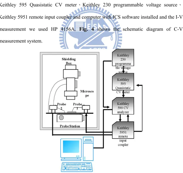
3.1 Measurement system setup
The system we used to measure the high ferquence capacitance is Bias
Temperature Stress measurement system (BTS): Keithley 590 CV analyzer 、
Keithley 595 Quasistatic CV meter、Keithley 230 programmable voltage source、 Keithley 5951 remote input coupler and computer with ICS software installed and the I-V measurement we used HP 4156A. Fig. 4 shows the schematic diagram of C-V
measurement system.
15
3.2 Capacitance fabrication
Current-voltage (I-V), capacitance-voltage (C-V) characteristics of SiO2 films were studied using a metal-oxide-semiconductor (MOS) capacitor structure. First the RCA clean was using for the removal of organic, metallic, and particulate contamination on the wafer surfaces. Then metal-oxide-semiconductor (MOS) structure with a Al/SiO2 stack on a p-type silicon substrate. The SiO2 was deposited using a mixture of N2O 75sccm , SiH4 5sccm ,Argon 75sccm at low substrate
temperature of 200 ℃ . The top and bottom electrodes of MOS capacitor was evaporated by E-gun evaporator.
3.3 Laser-activatied amorphous silicon (a-Si:H) and microcrystalline
silicon (uc-Si:H) self-aligned TFTs
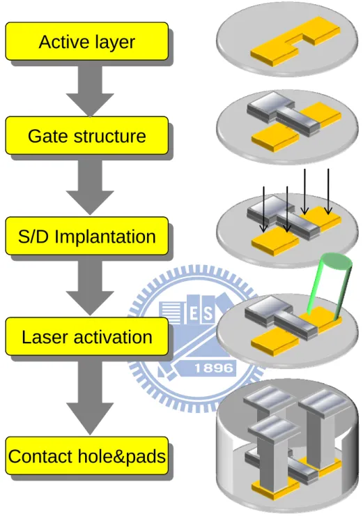
z Device fabrication flow
The device structure and fabrication flow chart show in Fig. 5
Step 1 . Active region formation. (1
stMask)
Using the HWCVD or HDPCVD to deposit amorphous silicon or microcrystalline silicon as 100nm on glass substrate. Then active region were defined by lithography process , that is first Mask. After lithography process, the patterned active region by RIE etching. After active region forming, acetone solution in
supersonic oscillator was used to remove photoresist.
Step 2 . Gate dielectric and Metal gate defined. (2
rdMask)
As source-drain had been formed , using the high density plasma chemical-vapor deposition system (HDPCVD) to deposited SiO2 100nm as gate dielectric. The SiO2
layer was deposited using mixture of SiH4 of 5 sccm, N2O of 75 sccm, and Argon of
25 sccm at pressure of 10mtorr and power of 300 watt, and substrate temperature 200OC was used. And then aluminum 250nm was evaporated by E-gun evaporator. After aluminum evaporated, gate region was defined by lithography process named
16
third Mask. Next, using RIE etcher to form gate structure ,then removed photoresist by acetone solution in supersonic oscillator. And it was known as self-aligned structure.
Step 3 . S/D Implantation and Laser activation
After gate structure was formed, S/D regions were implanted with phosphorus dose of 5×1015 cm-2 at an energy 35 keV for n-type TFT and activated by laser annealing(LA) at laser power of 3.3W. S/D regions must make sure the interface between silicon and metal as ohmic contact.
Step 4 . Passivation and Contact hole defined. (3
thMask)
Passivation is a process that using a certain thickness dielectric capping on the device to protect components from damage to the external environment. After gate structure was defined, SiO2 was used as passivation layer which was deposited 500nm
by HDPCVD. The third Mask was used to define contact hole in lithography process. Then contact hole structure was formed by RIE etcher. After contact hole region forming, acetone solution in supersonic oscillator was used to remove photoresist.
Step 5. Metal pads defined. (4
thMask)
After contact hole was defined, evaporating aluminum 500nm to contact gate, source and drain. And the final step, metal pads was patterned by fourth mask in in lithography process. Then gate, source and drain was isolated by RIE etcher. Finally, a top gate thin film transistor was compeleted.
17
Active layer
Active layer
Gate structure
Gate structure
S/D Implantation
S/D Implantation
Laser activation
Laser activation
Contact hole&pads
Contact hole&pads
Active layer
Active layer
Gate structure
Gate structure
S/D Implantation
S/D Implantation
Laser activation
Laser activation
Contact hole&pads
Contact hole&pads
18
3.4 In-situ dopant microcrystalline silicon TFTs
z Device fabrication flow
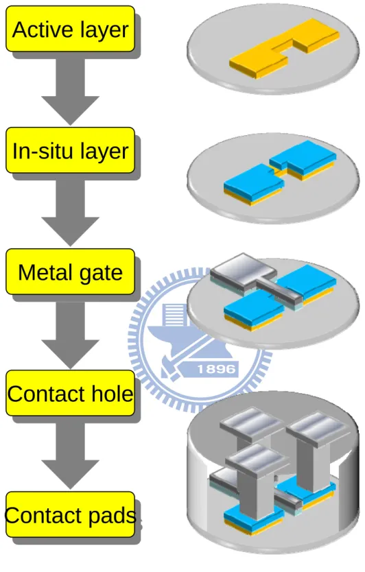
The device structure and fabrication flow chart show in Fig. 6
Step 1 . Active region formation. (1
stMask)
Using the HWCVD or HDPCVD to deposit amorphous silicon or microcrystalline silicon as 100nm on glass substrate. Then active region were defined by lithography process , that is first Mask. After lithography process, the patterned active region by RIE etching. After active region forming, acetone solution in
supersonic oscillator was used to remove photoresist.
Step 2 . n+ layer formation and source-drain isolation. (2
ndMask)
As active region defined, using HWCVD to deposite n+ nanocrystals silicon (nc-Si) layer 50nm. This layer made sure the interface between nc-Si and metal as ohmic contact. Before deposition n+ layer, native oxide was removed by wetting BOE (1:0) 10 sec. After deposition, the source-drain isolation was defined by lithography process. Then the source-drain was patterned by RIE etching. After source-drain region forming, acetone solution in supersonic oscillator was used to remove
photoresist.
Step 3 . Gate dielectric and Metal gate defined. (3
rdMask)
As source-drain had been formed , using the high density plasma chemical-vapor deposition system (HDPCVD) to deposited SiO2 100nm as gate
dielectric. The SiO2 layer was deposited using mixture of SiH4 of 5 sccm, N2O of 75
sccm, and Argon of 25 sccm at pressure of 10mtorr and power of 300 watt, and substrate temperature 200OC was used. And then aluminum 250nm was evaporated by E-gun evaporator. After aluminum evaporated, gate region was defined by lithography process named third Mask. Next, using RIE etcher to form gate structure ,then removed photoresist by acetone solution in supersonic oscillator.
19
Step 4 . Passivation and Contact hole defined. (4
thMask)
Passivation is a process that using a certain thickness dielectric capping on the device to protect components from damage to the external environment. After gate structure was defined, SiO2 was used as passivation layer which was deposited 500nm
by HDPCVD. The fourth Mask was used to define contact hole in lithography process. T h e n c o n t a c t h o l e s t r u c t u r e w a s f o r m e d b y R I E e t c h e r . After contact hole region forming, acetone solution in supersonic oscillator was used to remove photoresist.
Step 5. Metal pads defined. (5
thMask)
After contact hole was defined, evaporating aluminum 500nm to contact gate, source and drain. And the final step, metal pads was patterned by fifth mask in in lithography process. Then gate, source and drain was isolated by RIE etcher. Finally, a top gate thin film transistor was compeleted.
20
Active layer
Active layer
In-situ layer
In-situ layer
Metal gate
Metal gate
Contact hole
Contact hole
Contact pads
Contact pads
21
Chapter 4 Results and Discussions
4.1 CV measurement
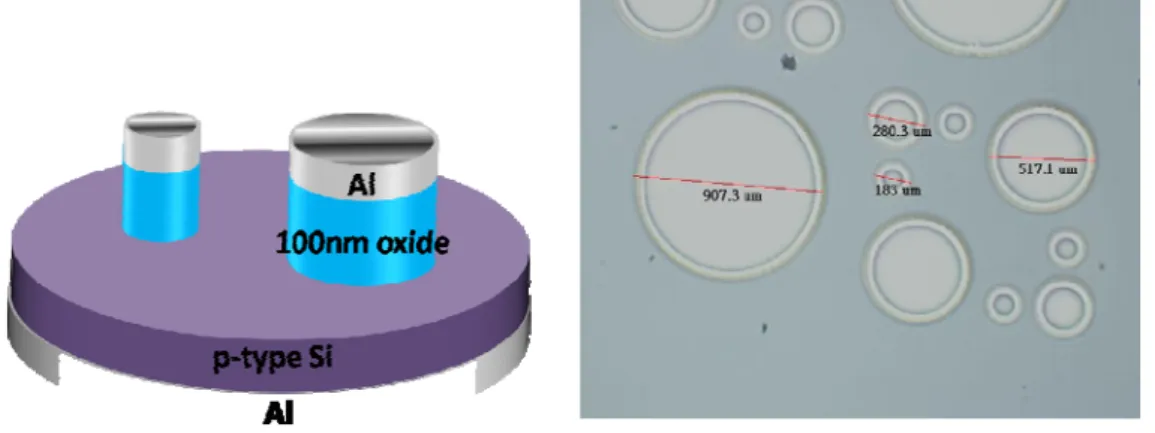
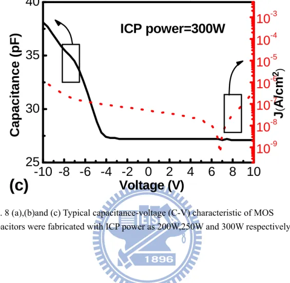
In order to test quality of gate oxide at low temperature of 200oC, test samples were deposited thickness of 100nm with three ICP power of 200,250 and 300W by HDPCVD. Schematic of metal-oxide-semiconductor (MOS) structure and top view shows in Fig. 7. Typical capacitance-voltage (C-V) characteristic of an metal-oxide-semiconductor (MOS) structure with a top circular Al pad, 400 μm in diameter, is presented in Fig. 8(a),(b) and (c) as ICP power of 200,250 and 300W respectively. All test capacitors were measured from -10V to 10V incremental 0.1V with high frequency of 100kHz. Although more efficient gas was dissociated with ICP power increasing, but more interface damage was increased from Ion bombardment. Fig. 8(c) shows a very noticeable effect of the interface traps is that the curves are stretched out in the voltage direction. This is due to the fact that extra charge has to fill the traps, so it takes more total charge or applied voltage to accomplish the same surface potential ψs, (or band bending).[1] Fig. 8(a)and (b) shows good C-V characteristic nearly, but Fig. 8(a) shows lower leakage current density than Fig. 8(b).
22
-10 -8 -6 -4 -2 0
2
4
6
8 10
25
30
35
40
Capacitance (pF)
Voltage (V)
10
-810
-710
-610
-510
-410
-3J
(A/
cm
2
)(a)
ICP power=200W
-10 -8 -6 -4 -2 0
2
4
6
8 10
10
20
30
Capaci
tance (pF
)
Voltage (V)
10
-910
-810
-710
-610
-510
-410
-3J
(A/
cm
2 )(b)
ICP power=250W
23
-10 -8 -6 -4 -2 0
2
4
6
8 10
25
30
35
40
Capacitance (pF)
Voltage (V)
(c)
ICP power=300W
10
-910
-810
-710
-610
-510
-410
-3J
(A/
cm
2 )Fig. 8 (a),(b)and (c) Typical capacitance-voltage (C-V) characteristic of MOS capacitors were fabricated with ICP power as 200W,250W and 300W respectively
24
4.2 Microcrystalline silicon film characterization
There were two intrinsic μc-Si:H films prepared by HDPCVD and HWCVD. First intrinsic μc-Si:H films were prepared by HDPCVD. The μc-Si:H thin films were deposited at the pressure 20mrott, ICP power of 450W, SiH4=10sccm ,H2=300sccm,substrate temperature of 200oC on the Si(100) wafer with
500 nm oxide and Corning glass substrate. Second intrinsic μc-Si:H films were prepared by HWCVD. The μc-Si:H thin films were deposited at the pressure 10mrott on the Si(100) wafer with 500 nm oxide and Corning glass substrate. For the hot wire we used 4-5 coiled tungsten filaments with 0.5 mm in diameter, the distance between the filament and substrate of 4.5cm, the filament temperature of 1800oC ,SiH4=10sccm,H2=130sccm and the substrate temperature of 200oC.
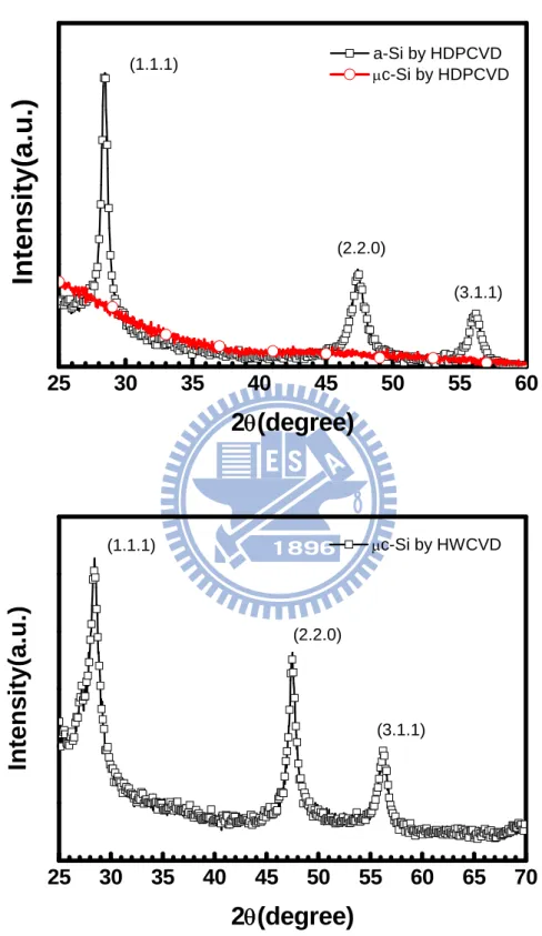
Fig. 9(a),(b) shows the XRD spectra of μc-Si:H by HDPCVD and HWCVD respectively.The diffraction peaks for (111), (220), and (311) planes are visible for the films deposited on the Si substrate and the preferred orientation is (111). Fig. 10(a) shows the TEM image of intrinsic μc-Si:H by HDPCVD. In Fig. 10(b), it shows clearly that incubation layer of 20nm. Fig. 11(a)-(b) shows the plane-view SEM images of intrinsic and n-type deposited on the Si substrate with 5000Å oxide at a substrate temperature of 200 oC by HWCVD. It reveals that the μc-Si:H films consisted of a large amount of granular grains as shown in Fig. 11(a) and (b). The cross-section of μc-SiH i-layer films structure also was shown in Fig. 11(c) It clearly demonstrated that the column μc-Si:H structure with a grain sizes of ~50-100 nm and a column grain height of ~100-300 nm were grown vertically on the substrate. In addition, the deposition rate of μc-Si:H films with large grain sizes was about 5-7 Å/s, which was higher than traditional plasma system, such as PECVD [2]. It considered that the efficient catalytic decomposition of precursor gases at the heated metal filaments [3], good gas utilization (>75%) [2, 4, 6], and thus high deposition rates are
25
achieved using HWCVD. Whatever, the column structures of μc-Si:H is still advantage of the transport of carriers [7-8]. To verify this benefit of column structure from μc-Si:H, the μc-Si:H TFTs has been fabricated.
26 25 30 35 40 45 50 55 60 (3.1.1) (1.1.1) a-Si by HDPCVDμ c-Si by HDPCVD
2
θ
(degree)
In
te
n
s
it
y
(a.u
.)
(2.2.0) 25 30 35 40 45 50 55 60 65 70 (3.1.1) (2.2.0) μc-Si by HWCVDIntensity(a.u.)
2
θ
(degree)
(1.1.1)27
Fig. 10 (a)TEM image of μc-Si:H by HDPCVD (b) Incubation layer of 20nm
H
μc-Si:H
28
Fig. 11 (a), (b) Plane-view SEM images of intrinsic and n-type μc-Si:H (c) The cross-section of μc-SiH i-layer films structure by HWCVD
(b)
(a)
(c)
(c)
29
4.3 Highly conductive doped flim
In order to made sure the interface between n+nc-Si and metal as ohmic contact. A metal-semiconductor (MS) device was fabricated with Al/n+nc-Si:H stack on 500nm oxide on silicon wafer. Schematic of MS device shows in Fig. 12 The resistance is expressed as t W L A L R ⋅ =
=ρ ρ , where ρ is resistivity, L is length , W
is electrode width, t is thickness of film respectively. We design the length between two electrodes equal to the width of electrode, then the resistivity ρ is simplification into ρ=t×R. The resistance R can be extracted by fitting the I-V curve. The
n+nc-Si:H was deposited at process pressure 5mtorr, SiH4=3sccm,H2=36sccm, diluted
PH3=1,2,3,5and 8% and the filament temperature of 1700oC by HWCVD. Fig.
13(a),(b) shows resistivity of undoped and difference doped films respectively. According to these results, the n+nc-Si:H with doped PH3=3% was chosen for S/D
of the in-situ doped TFTs.
30 -6 -4 -2 0 2 4 6 -5 0 5 I(pA) Voltage(V) ρ=1.56X10⁷Ω-cm
(a)
0 1 2 3 4 5 6 7 8 9 10-2 10-1 100 101 102 103 104 105 106 Re sistivity ( Ω− cm) PH3 dopant(%)(b)
Fig. 13 (a) IV-curve of Intrinsic nc-Si;H film (b) Resistivity of n+nc-Si:H with different PH3 dopant
31
4.4 IV characterization and Density of states of laser-activated
self-aligned TFTs
To extract density of states of amorphous/microcrystalline silicon by FEC method from TFTs, three different active layer channel of TFTs with 100nm oxide layer as gate dielectric was fabricated as illustrated on Fig. 14. And Fig. 14(a) and (b) are amorphous and microcrystalline active channel layer by HDPCVD. Fig. 14(c) is microcrystalline active layer by HWCVD Fig. 15(a) , (b) shows transfer and output characteristics curves of amorphous silicon active layer TFTs with a channel width of 20 um and a channel length of 15um by HDPCVD. The transfer characteristics curves applied Vg varied from 0 V to 15V with an increment of 0.1 V while the drain voltage
VD was kept constant at 1 V. As the Vg changed from 0V to +15V, the device switches
from the off state to the on state with the threshold voltage 8V. The field-effect electron mobility (μeFE) is calculated from the transconductance of the TFT operating
in the linear regime at VD = 1 V, μeFE=(∂ID/∂VG)(L/CoxVDW), where ∂ID / ∂VG, Cox,
and L/W are the transconductance, the a-SiOx gate dielectric capacitance per unit area, and the TFT channel length to width ratio, respectively.It is seen that the maximum value of μeFE is 0.22 cm2/V-s. The sub-threshold slope is 0.45 V/decade and the
ON/OFF current ration more than 104. Fig. 16(a) , (b) shows transfer and output
characteristics curves of microcrystalline silicon active layer TFTs by HDPCVD with a channel width of 4 um and a channel length of 15um at VD=1V. The maximum
value of μeFE is 3.62 cm2/V-s. The sub-threshold slope is 0.33 V/decade and the
ON/OFF current ratio more than 105. Fig. 17(a), (b) shows transfer and output characteristics curves of microcrystalline silicon active layer TFTs with a channel width of 15 um and a channel length of 8um by HWCVD at VD=1V. The maximum
value of μeFE is 16.26 cm2/V-s. The sub-threshold slope is 0.25 V/decade and the
32
In order to extract density of states from Field Effect Transconductance (FEC) method, flat-band voltage was required. So we measure these three different TFTs at different temperature from 25oC to 150oC with an incremental of 25oC. Fig. 18 shows the density of states which were extracted from three different active channel layer TFTs.
The crystallinity of the active channel pay an important role to relate to electrical characteristics of amorphous/microcrystalline TFTs. The field-effect mobility of amorphous/microcrystalline TFTs in the Fig. 15 (a),Fig. 16(a) and Fig. 17(a) is enhanced from 0.22-16.26 cm2/V-s as the crystallinity increasing. The results indicate that the crystallinity are improved by degrees. In addition, the reduction of threshold voltage with increasing crystallinity is due to decrease the grain boundaries of active channel layer. It also shows that subthreshold swing slope is lowered initially from 0.45 V/decade to 0.25 V/decade. Since the subthreshold swing slope is usually made use of estimating the interface trap density in standard MOSFET technology. In poly TFTs, the subthreshold swing slope is controlled by both bulk trap states and interface trap density near mid-gap [8]. The subthreshold swing slope S of poly-Si TFTs is given by ⎟⎟ ⎠ ⎞ ⎜⎜ ⎝ ⎛ + + ⋅ ⋅ = ox ts D C C C q kT S ln10 1 Eq.4-1
Where Cox is the oxide capacitance per unit area, CD is the depletion layer capacitance
per unit area, and Cts=q2Dts , where Dts (ev-1cm-2) is the density of total trap states in the
vicinity[1] of the intrinsic Fermi level. In poly-Si TFTs. The density of trap states near mid-gap Dts includes both bulk trap density Dbulk and interface trap density Dit. Since
the poly-Si film is thin and intrinsic, CD《 Cts and the subthreshold swing slope of
33 ⎟⎟ ⎠ ⎞ ⎜⎜ ⎝ ⎛ ⋅ + ⋅ ⋅ = ⎟⎟ ⎠ ⎞ ⎜⎜ ⎝ ⎛ + ⋅ ⋅ = ox ts ox ts C D q q kt C C q kt S 2 1 10 ln 1 10 ln Eq.4-2
Considering that in a first approximation the devices are fully depleted, i.e., the energy band bending occurs over the whole poly-Si film thickness, the Dts can be approximated
as it Si bulk ts D t D D = ⋅ + Eq.4-3
Where Dbulk is the mean bulk trap density, tSi is the poly-Si film thickness, and Dit is the
interface trap density.
Following above equations, subthreshold swing slope of poly-Si TFTs is reflected by bulk trap density and interface trap density. As the grain boundaries defects are terminated by increasing crystallinity, the subthreshold swing slope is decreased.
34
Fig. 14 Schematic cross section of self-aligned amorphous/microcrystalline silicon TFT.
35 0 2 4 6 8 10 12 14 10-13 10-12 10-11 10-10 10-9 10-8 0 1 2 3 4 5 6 7 8 9 10
T
ransconductance(nA/V
)
I
d(A)
V
g(V)
Vd=1V W=20 μm L=15μm μn=0.220 cm-2/V-S V th=8V SS=0.45 V/decade(a)
0 2 4 6 -2 0 2 4 6 8 10 12 14 16 Vg=6 V Vg=8 V Vg=10 V Vg=12 V Vg=14 VI
d(nA)
V
d(V)
(b)
Fig. 15 (a) Transfer and (b) output characteristics of amorphous silicon n-type TFTs by HDP-CVD
36
-2
0
2
4
6
8
10 12 14
10
-1310
-1210
-1110
-1010
-910
-810
-70
2
4
6
8
10
12
14
16
18
20
Transconduct
ance(nA/
V
)
I
d(A)
V
g(V)
Vth=3.7 V μn=3.62 cm2/V-S ss=0.33 V/decade W=4μm L=15μm(a)
0
2
4
6
8
10
0.0
0.1
0.2
0.3
0.4
0.5
0.6
Vg=2 V Vg=6 V Vg=10 VI
d(
μ
A)
V
d(V)
(b)
Fig. 16 (a) Transfer and (b) output characteristics of microcrystalline silicon n-type TFTs by HDP-CVD
37
-2
0
2
4
10
-1410
-1310
-1210
-1110
-1010
-910
-810
-710
-610
-510
-40.0
0.5
1.0
1.5
Transconductance(
μ
A/V)
I
d(A)
V
g(V)
Vth=2.2 V μn=16.26 cm2/V-S ss=0.25 V/decade W=15μm L=8μm(a)
0
1
2
3
0
2
4
6
8
10
Vg=0.1 Vg=2 Vg=4Id(
μ
A)
Vd(V)
(b)
Fig. 17 (a) Transfer and (b) output characteristics of microcrystalline silicon n-type
38
0.0
0.1
0.2
0.3
0.4
0.5
10
1610
1710
1810
1910
2010
2110
2210
23 a-Si by HDPCVD nc-Si by HDPCVD μc-Si by HWCVDDO
S
(eV
-1cm
-3)
E-E
F(eV)
Fig. 18 The density of states distribution of amorphous/microcrystalline TFTs were extracted from Field Effect Conductance (FEC) method.
39
4.5 IV characterization and Density of states of In-situ dopant TFTs
For the purpose of suitable for flexible display, low temperature TFTs without S/D implantation is necessary. So the highly conductance doped layer is required that the interface between nc-Si and metal is ohmic contact. This type of TFTs was called In-situ dopant TFTs. A TFTs with a microcrystalline active layer of 100nm, in-situ doped layer of 50nm and oxide as gate dielectric of 100nm was fabricated as illustrated on Fig. 19. The TFTs with a channel width of 10 um and a channel length of 60um was fabricated on microcrystalline silicon layer on glass substrate. Fig. 20
(a) , (b) shows transfer and output characteristics curves of in-situ doped TFTs by HDPCVD. The maximum value of μeFE is 50.2 cm2/V-s. The sub-threshold slope is
0.157 V/decade and the ON/OFF current ratio more than 104. Fig. 21 (a) , (b) shows transfer and output characteristics curves of in-situ doped TFTs by HWCVD. The maximum value of μeFE is 19.26 cm2/V-s. The sub-threshold slope is 0.097 V/decade
and the ON/OFF current ratio more than 104. The density of states distribution shows in Fig. 22 which was extracted from in-situ doped TFTs by FEC method. Fig. 23
(a) ,(b)shows schematic three-dimensional of in-situ doped TFTs and top view. Defect density associated with the deep state in the silicon energy bandgap exerted a significant influence on the off-state current, and the density related to tail state governed the on-state current.[9] Fig. 22 shows the corresponding density of states distribution fitted to the curves in Fig. 20(a) and Fig. 21(a). The density at the midgap is almost the same order of magnitude. The subthreshold swing slope is also related to midgap defect. Fig. 20(a) and Fig. 21(a) show low subthreshold swing slope of 0.097 and 0.14 V/decade , because defects at midgap is low(the deep state). The electron mobility could be improved from 19.26 to 50.2 cm2/V-s due to the reduction of gap state near the conduction band edge or decrease in the slope of gap state near the conduction band edge.[10]
40
Fig. 19 Schematic cross-section of a standard n-channel top-gate staggered nc-Si:H TFT with n+ nc-Si:H ohmic contacts.
41 -6 -4 -2 0 2 4 6 8 10 12 10-12 10-11 10-10 10-9 10-8 10-7 10-6 10-5 0.00 0.05 0.10 0.15 0.20 0.25 0.30 0.35 0.40 0.45 0.50
Transconduct
a
nce(
μ
A/V)
I
d(A
)
V
g(V)
Vd=1V W=10 μm L=60μm μ n=50.2 cm 2 /V-S Vth=3.2V SS=0.157 V/decade 0 2 4 6 8 10 -2 0 2 4 6 8 10 12 14 16 18 20 Vg=4 V Vg=6 V Vg=8 V Vg=10 VI
d(
μ
A)
V
d(V)
(b)
Fig. 20 (a) Transfer and (b) output characteristics of amorphous silicon n-type TFTs
42 -6 -4 -2 0 2 4 6 8 10 12 10-13 10-12 10-11 10-10 10-9 10-8 10-7 0.0 0.1 0.2 0.3
T
ransconduct
a
nce(
μ
A/V)
I
d(A)
V
g(V)
Vd=0.1V W=40 μm L=40μm μn=19.26 cm2/V-S Vth=1.9 V SS=0.097 V/decade(a)
0 2 4 6 8 10 -0.5 0.0 0.5 1.0 1.5 2.0 2.5 3.0 3.5 4.0 4.5 5.0 Vg=4 V Vg=6 V Vg=8 V Vg=10 VI
d(
μ
A)
V
d(V)
Fig. 21(a) Transfer and (b) output characteristics of amorphous silicon n-type TFTs by HWP-CVD
43
0.0
0.1
0.2
0.3
0.4
0.5
10
1610
1710
1810
1910
2010
2110
2210
2310
24 μc-Si by HDPCVD μc-Si by HWCVDDOS(eV
-1cm
-3)
E-E
F(eV)
Fig. 22 The density of states distribution of in-situ doped TFTs were extracted from Field Effect Conductance (FEC) method.
Fig. 23 (a) ,(b)shows schematic three-dimensional of in-situ doped TFTs and top view
44
Chapter 5 Conclusions and Future work
5.1 Conclusions
In summary, top-gate microcrystalline silicon TFTs were realized at maximum process temperature of 200 °C with high electron charge carrier mobilities exceeding 50 cm2 /V-s ,and on/off ration exceeding 104 under low voltage operation at VD=0.1V.
The VT and the subthreshold swing are in the range of 1.8-2.5 V and 0.1-0.45
V/decade, respectively. The experimental results reveal that the highest charge carrier mobility and the lowest defect density are obtained when the intrinsic microcrystalline silicon channel material is grown by HDPCVD and HWCVD. Microcrystalline silicon allows for the low temperature integration of high performance TFTs on glass and plastic substrates.
5.2 Future work
The flexible electronics on plastic substrates possess advantageous characteristics, being lightweight, durable, flexible, and have the capacity to be manufactured in a variety of shapes, which leads to freedom of design. Furthermore, the in-situ dopant TFTs use the same material as thin film solar cell, so we can integrate these two devices as new generation green display technology.
45
Reference
Chapter 1
[1]. Weimer, P. K. (1962). "The TFT A New Thin-Film Transistor." Proceedings of the IRE 50(6): 1462-1469.
[2].le Comber, P. G., W. E. Spear, et al. (1979). "Amorphous-silicon field-effect device and possible application." Electronics Letters 15(6): 179-181.
[3]Depp, S. W., A. Juliana, et al. (1980). Polysilicon FET devices for large area input/output applications.
[4]Little, T. W., K. Takahara, et al. (1991). "Low temperature poly-Si TFTs using solid phase crystallization of very thin films and an electron cyclotron resonance chemical vapor deposition gate insulator." Japanese Journal of Applied Physics 30(part 1): 3724-3728.
[5] R. B. Min and S. Wagner, Appl. Phys. A, 74, 541 (2002) [6]Y. Chen and S. Wagner, Appl. Phys. Lett. 75, 1125 (1999)
[7] M. Mulato, Y. Chen, S. Wagner, and A. R. Zanatta, J. Non-Cryst. Solids, 266, 1260 (2000)
[8]S. Veprek, Z. Iqbal, R. O. Kuhne, P. Capezutto, F. A. Sarott, and J. K. Gimzewski, J. Phys. C: Solid State Phys. 16, 6241 (1983)
[9] A. Saboundji, N. Coulon, A. Gorin, H. Lhermite, T. Mohammed-Brahim, M. Fonrodona, J. Bertomeu and J. Andreu, Thin Solid Films, 487, 227 (2005). [10] S. Wagner, H. Gleskova, I-C. Cheng, and M. Wu, Thin Solid Films, 430, 15 (2003)
[11] J. Jang, J. Y. Oh, S. K. Kim, Y. J. Choi, S. Y. Yoon, and C. O. Kim, Nature sLondond 395, 481 (1998).
46
and I. French, J. Appl. Phys. 86, 7079 (1999).
[13] T. Nagahara, K. Fujimoto, N. Kohno, Y. Kashiwagi, and H. Kakinoki, Jpn. J. Appl. Phys., Part 1 31, 4555 (1992).
[14] I-C. Cheng and S. Wagner, Appl. Phys. Lett. 80, 440 (2002)
Chapter 2
[1]. Jerzy Kanicki, Amorphous and Microcrystalline Semiconductor Devices VolumeІІ.
[3] K. Y. Chan, D. Knipp, A. Gordijn, and H. Stiebig, Journal of Applied Physics 104, 054506 (2008).
[2] O. Vetterl, F. Finger, R. Carius, P. Hapke, L. Houben, O. Kluth, A. Lambertz, A. Mück, B. Rech, and H. Wagner, Sol. Energy Mater. Sol. Cells 62,97 2000 [4] C. C. Tsai, in Amorphous Silicon and Related Materials, edited by H.
Fritzche sWorld Scientific, Singapore, (1988), p. 123. [5] A. Matsuda, J. Non-Cryst. Solids 59–60, 767 (1983).
[6] G. Yue, J. D. Lorentzen, J. Lin, D. Han, and Q. Wang, Applied Physics Letters
75, 492-494 (1999).
[7]. A. Matsuda and T. Goto, Mater. Res. Soc. Symp. Proc. 164, 3(1990) [8]. A. Matsuda, Thin Solid Flims 337, 1(1999)
[9]. S. Veprek, Z.Iqbal, H.R.Oswald, and A. P.Wedd, J. Phys. C 14, 295(1981) [10]. C.C. Tsai, G. B. Anderson, R. Thompson, and B. Wecker, J. Non-Cryst. Solids
114, 151(1989)
[11]. I. Shimizu, J. Non-Cryst. Solids114, 145(1989)
[12]. G. Fortunato and P. Migliorato, Appl. Phys. Lett., 49, 1025 (1986). [13] S. Hirae, M. Hirose and Y. Osaka, J. Appl. Phys., 51, 1043 (1980).
[14] H. C. de Graaf, M. Huyber and J. G. de Groot, Solid state Electron. 25, 67 (1982).
47
[15] R. L. weisfield and D. A. Anderson, Philos Mag. B., 44, 83 (1981).
[16] G. Fortunato, D. B. Meakin, P. Migliorato and P. G. Lecomer, Philos. Mag. B., 57,573 (1988).
[17] T. Suzuki, Y. Osaka and M. Hirose, Jpn. J. Appl. Phys., 21, L159 (1982).
Chapter 4
[1]S. M. S. Kwok K. Ng, "Physics of Semiconductor Devices,3rd Edition," (2007). [2] N. Honda, A. Masuda, H. Matsumura, J. Non-Cryst. Solids. 266, 100 (2000). [3] R.E.I. Schropp, S Nishizaki, ZS Houweling, V Verlaan, C.H.M. van der Werf, H Matsumura, Solid State Electron. 52, 427 (2008).
[4 ] S.G. Ansari, H. Umemoto, T. Morimoto, K. Yoneyama, A. Izumi, A. Masuda, H. Matsumura, Thin Solid Films. 501, 31 (2006)
[5] K. Ishibashi, Thin Solid Films. 395, 55 (2001).
[6]K. Y. Chan, D. Knipp, A. Gordijn, and H. Stiebig, J. Appl. Phys. 104, 054506 (2008).
[7]A. Saboundji, N. Coulon, A. Gorin, H. Lhermite, T. Mohammed-Brahim, M. Fonrodona, J. Bertomeu, J. Andreu, Thin Solid Films. 487, 227 (2005).
[8].T. Noguchi, Jpn. J. Appl. Phys., Part 2 32, L1584 (1993).
[9] K. Ono, T. Aoyama, N. Konishi, and K. Miyata, "Analysis of current voltage characteristics oflow-temperature-processed polysilicon thin-film transistors," IEEE Transactions on Electron Devices, vol. 39, pp. 792-802, (1992).
[10] T. Suzuki, M. Hirose, and Y. Osaka, "Influence of Gap States on Basic
Characteristics of a-Si: H Thin Film Transistors," Japanese Journal of Applied Physics, vol. 21, pp. L315-L317, (1982)
![Table 1. Status of silicon materials for TFTs [10]](https://thumb-ap.123doks.com/thumbv2/9libinfo/8621931.191600/12.892.139.759.285.472/table-status-silicon-materials-tfts.webp)