國 立 交 通 大 學
電子工程學系 電子研究所
博 士 論 文
應用於高密度資料儲存與軟性電子之交錯電
阻式記憶體
Cross-point Resistive Switching Memory for
High-density Data Storage and Flexible Electronics
研 究 生:黃 俊 嘉
指導教授:侯 拓 宏 博士
雷 添 福 博士
應用於高密度資料儲存與軟性電子之交錯電
阻式記憶體
Cross-point Resistive Switching Memory for
High-density Data Storage and Flexible Electronics
研 究 生:黃俊嘉
Student:Jiun-Jia Huang
指導教授:侯拓宏 博士
Advisor:Dr. Tuo-Hung Hou
雷添福 博士
Dr. Tan-Fu Lei
國立交通大學
電子工程學系 電子研究所
博士論文
A Dissertation
Submitted to Department of Electronics Engineering
and Institute of Electronics
College of Electrical and Computer Engineering
National Chiao Tung University
In Partial Fulfillment of the Requirements
For the Degree of
Doctor of Philosophy
in
Electronics Engineering
October 2012
Hsinchu, Taiwan, Republic of China
應用於高密度資料儲存與軟性電子之交錯電阻
式記憶體
學生: 黃 俊 嘉
指導教授: 侯 拓 宏 博士
雷 添 福 博士
國立交通大學
電子工程學系 電子研究所博士班
摘 要
利用電阻式記憶體 (RRAM)所組成的被動型陣列 (passive array) 雖具有最小單元
面積 4F2 的優異微縮潛力,但位元間的讀取干擾 (read interference) 造成讀取窗口
(read margin) 對整個陣列上的非選取記憶單元 (unselected cells) 儲存狀態有相當程度 的相依性,並嚴重地限制了記憶體陣列尺寸的設計,因此開發能適用於電阻式記憶體 的選擇元件 (selection device) 是一個非常值得研究的議題。考慮到能與電阻式記憶體 匹配的元件,以氧化物為基礎 (oxide-based) 的選擇元件結構簡單、製程微縮容易並可 直接與電阻式記憶體形成垂直堆疊結構,是目前最為可行的候選。此論文探討了在室 溫環境下,開發出分別適用單極切換 (unipolar RRAM) 與雙極切換 (bipolar RRAM) 的 氧化物選擇元件並針對在交錯型陣列 (crossbar array) 所遇到的問題來做完整分析。
首先,我們利由 Ti/TiO2與 TiO2/Pt 介面的蕭基能障特性,成功地在室溫環境下製
氧離子隨外加偏壓會有不均勻分佈的移動,使得這些氧缺 (oxygen vacancy) 所造成的 局部傳導路徑 (filament) 促使二極體元件擁有相當高的順向電流。接著,由於 Ti/TiO2/Pt 二極體優異的低溫整合能力,我們可以將二極體與 Ni/HfO2/Pt 記憶體元件整合至可撓 式基板 (flexible substrate) 上進一步去驗證 1D1R 架構的單極電阻切換特性,其高整流 開關比與穩定的切換特性可以實現至512 Kb 大小的記憶體容量。 另一方面,我們也針對雙極切換的電阻式記憶體開發出適用的選擇器 (selector)。 由於雙極的切換特性,雙極性選擇器需具有足夠高的雙向導通電流去達成組態切換的 需求與高非線性程度 (nonlinearity) 去抑制讀取干擾。因此,我們藉由 Ni/TiO2介面的 蕭基能障所控制的非線性電流-電壓特性製作出對稱結構的 Ni/TiO2/Ni 選擇器。在阻態
切換特性方面,我們使用了Ni/TiO2/Ni 選擇器與 Ni/HfO2/Pt 記憶體元件去驗證 1S1R 雙
極切換能力。除了1S1R 較穩定的雙極切換特性之外,藉著簡單的預測模型,我們也發
現1S1R 比 1D1R 俱有更優異的應用潛力。
最後,實驗的結果顯示,Ni/HfO2/Pt 記憶體元件應用到軟性基板下可以承受高度彎
曲 (bending) 、 超 過 106 次 的 操 作 容 忍 度 (endurance) 與 快 於 100 奈 秒 的 操 作
(SET/RESET) 速度。藉由等效電路的計算結果,我們開發出高導通電流密度 (~105
A/cm2) 與高非線性程度 (~103) 的 Ni/TiO2/Ni 選擇器擁有應用到兆位元級記憶容量的
潛力。另外,由於氧化物元件優異的低溫整合能力,我們也成功的將垂直整合結構
Ni/TiO2/Ni/HfO2/Pt 驗證到 8 × 8 的軟性記憶體陣列上,並可以明確的判讀出陣列中記
憶體元件的高低組態。我們相信此篇論文的研究成果可以提供未來應用在高效能軟性 記憶體設計的重要研究方向。
Cross-point Resistive Switching Memory for
High-density Data Storage and Flexible Electronics
Student: Jiun-Jia Huang
Advisor: Dr. Tuo-Hung Hou
Dr. Tan-Fu Lei
Department of Electronics Engineering &
Institute of Electronics
National Chiao Tung University
ABSTRACT
Cross-point RRAM with 4F2 cell size has attracted a great attraction because of its superior scalability. However, read interference between neighboring cells in passive arrays has become a serious issue, where the read margin depends strongly on the stored patterns of the unselected cells. This may significantly limit the maximum available array size. Therefore, it is in urgent need to design a suitable selection device for crossbar RRAM to improve read margin but without sacrificing high cell density. Considering the process compatibility, oxide-based selection devices is a promising candidate to reduce the sneak current because of its simple structure, excellent scalability and low-temperature processes allowing vertically stacking with RRAM. In this thesis, we introduced two selection devices
compatible with room-temperature process for unipolar RRAM and bipolar RRAM, respectively.
Firstly, we fabricated a room-temperature Ti/TiO2/Pt oxide diode with an excellent
rectifying characteristic by the asymmetric Schottky barriers at the Ti/TiO2 and the TiO2/Pt
interfaces. The experimental results show that the current transport was governed by the localized oxygen-deficient TiO2 filaments, which contributes the high forward current in the
Ti/TiO2/Pt oxide diode. Furthermore, a flexible one diode-one resistor (1D1R) memory cell,
consisting of Ti/TiO2/Pt diode with a large rectifying ratio and a stable unipolar
resistive-switching (RS) Ni/HfO2/Pt memory element, was fabricated using only
room-temperature processes. Due to its superior rectification ratio of 1D1R cell, it can effectively realize a crossbar array as large as 512 Kb.
On the other hand, a nonlinear selector for bipolar RRAM in the crossbar array was fabricated using a simple Ni/TiO2/Ni metal-insulator-metal (MIM) structure. The highly
nonlinear current-voltage characteristics were realized by the Schottky barrier at Ni/TiO2
interfaces. The series connection with a HfO2 resistive memory shows a reproducible bipolar
RS. Predicted by a simple analytical calculation, one selector-one resistor (1S1R) cell shows even more promising potential as compared with the 1D1R cell.
Finally, the flexible Ni/HfO2/Pt memory element with superior properties, including
excellent immunity to mechanical bending, reliable cycling and fast SET/RESET speed were demonstrated. Additionally, a flexible Ni/TiO2/Ni selector with a high current density of 105
A/cm2 and highly nonlinear I-V was capable of gigabit memory arrays implementation. We eventually realized a vertically stacked Ni/TiO2/Ni/HfO2/Pt 1S1R cell on a flexible 8 × 8
crossbar array, where the HRS/LRS states of the selected cell were successfully read out. We believe that our research provides a clear path for future high-performance flexible memory applications.
Acknowledgments
從碩士班開始歷經了八年時光、兩種時期,沒有眾人的鼓勵與幫助就無法順利完 成此論文。首先,感謝我的兩位指導教授-雷添福博士的指導與教誨,更重要的是教 導我待人處世之道;侯拓宏博士在我研究遇到瓶頸時提供非常多的指導與幫助,讓我 學習到非常珍貴的研究方法與態度,是我非常尊敬的人生導師。 感謝實驗室各位學長們:楊紹明學長、林育賢學長、張家文學長帶我進入記憶體 的領域;陳志仰學長有條有理的做事態度;愛批判卻又中肯的鄧志剛學長;感謝一起 合作過的學弟明爵、文彥、志偉、緯宸、奕銘和淳立,一起經歷過跑實驗、量測與討 論,提供我相當大的協助。 感謝曾給我幫助的前輩們,特別是奈米中心的陳悅婷小姐的關心與提供人生莫大 的指引;感謝陳明麗小姐、林聖欽先生、胡進章先生、黃國華先生在儀器的維護上提 供幫助;感謝何惟梅小姐、陳思穎小姐與楊月嬌小姐在行政程序上的協助以及國家奈 米元件實驗室的工程師們,因為有你們的幫忙,讓我在研究及學習上事半功倍。 感謝在309C 實驗室一起相處過的成員:喜愛拍照的郭柏儀學長、謝明山學長、陸 志誠學長、游信強學長、王獻德學長、陳建豪學長,感謝你們適時的給我幫助與勉勵; 感謝同窗及好友們:愛講心事的振昌、源竣、桑學長、統億、錦石、宗元、伯浩、梓 翔、當了 N 年室友的仕傑、客家一哥文呈、健談的冠良、善解人意的怡婷、一起享受 打球時光的崇威與新鈞、哲綸、久騰、榮家、文緯,在課業上的砥礪及分享生活上的 樂趣;實驗室可愛的學弟妹們:志竤、嘉塵、羅傑、顯琮、旺駿、仁傑、國譯、冠龍、 朝淵、妍君、鈺芬、玫瑾、群策、力仁、邦軒,實驗室因為有你們而充滿歡樂與溫馨; 感謝在美國這段期間幫助過我的人,特別是愛荷華大學的林教授夫婦與Hassan 教授夫 婦,在此獻上我最深的敬意。 感謝我親愛的家人,弟弟俊諺,在學業與生活上給我莫大的關心與扶持。最後由 衷感謝我敬愛的母親蔡綉梅女士,身兼父職的拉拔兩個孩子長大,並且提供一個溫暖 的家。由於您無私的付出,我才能順利地完成學業。 於 風城交大 Oct. 16, 2012Contents
Abstract (Chinese) ………...………I
Abstract (English) ……….III
Acknowledgments………….………...V Contents ………...VI Table Lists………...IX Figure Captions………...…………X
Chapter 1 Introduction...1
1.1 Background..…….……….……….….… 11.2 Development of Resistive-Switching RAM (RRAM)……….….…...2
1.2.1 Basic concepts of RRAM………..3
1.2.2 Development of selection devices for crossbar RRAM……….4
(a) One Transistor - One Resistor (1T1R)……….5
(b) One Diode - One Resistor (1D1R)……….……..5
(c) Complementary Resistive Switching (CRS)………6
(d) One Selector - One Resistor (1S1R)………7
1.2.3 Operation methods of crossbar RRAM……….8
(a) “Write” operation……….8
(b) “Read” operation………..9
1.1 Motivation……….…….10
1.2 Thesis Organization………11
2.1 Introduction………25
2.2 Experimental Procedure……….26
2.3 Results and Discussion………...27
2.3.1 Current-voltage characteristics of Ti/TiO2/Pt diode………27
2.3.2 Physical characteristics of Ti/TiO2/Pt diode………28
2.3.3 Conduction mechanism………....29
2.3.4 Rectifying mode to resistive-switching mode……….30
2.4 Summary……….31
Chapter 3 Ti/TiO
2/Pt Oxide Diode for 1D1R Resistive-Switching Memory
on Flexible Substrates……….……….41
3.1 Introduction ……….……….………...………..41
3.2 Experimental Procedure……….42
3.3 Results and Discussion………...43
3.3.1 Flexible Ti/TiO2/Pt diode……….43
3.3.2 Pt/TiO2/Pt memory element and monolithic TiO2 1D1R cell………..………44
3.3.3 Ni/HfO2/Pt memory element and heterogeneous HfO2-TiO2 1D1R cell...45
3.3.4 Prediction on read margin in 1D1R crossbar array………..46
3.4 Summary………..………...47
Chapter 4 Bipolar Nonlinear Ni/TiO
2/Ni Selector for 1S1R Crossbar
Array Applications……….……..61
4.1 Introduction……….………...61
4.2 Comparison of 1D1R and 1S1R Crossbar Arrays……….…….……62
4.3 Device Fabrication Process……….…...63
4.4.1 I–V characteristics of bipolar Ni/TiO2/Ni selector….………..63
4.4.2 Bipolar 1S1R resistive switching……….………64
4.4.3 Read margin analysis……….………..65
4.5 Summary……….67
Chapter 5 1S1R Crossbar Array for Low-cost Flexible Electronic
Applications………..77
5.1 Introduction………77
5.2 Experimental Procedure……….78
5.3 Results and Discussion………...………79
5.3.1 Flexible Ni/TiO2/Ni and Ni/HfO2/Pt………79
5.3.2 Flexible and vertically stacked 1S1R array………….………..81
5.4 Summary……..………...………82
Chapter 6 Conclusion and Further Recommendation...97
6.1. Conclusion...……….………….………...97
6.2. Further Recommendation...……….……….………..99
Table Lists
Chapter 1
Table 1.1 Comparison of various unit cell structures for RRAM……….…14
Chapter 4
Figure Captions
Chapter 1
Fig. 1.1 Emerging memories based on the cross-point structure for future low-cost and high-performance memory applications. ………..………….…15 Fig. 1.2 Examples of flexible electronics: (a) prototype of the flexible e-paper display [10], (b) photograph image of the flexible circuit and the flexible antenna [11], (c) a bendable cell phone [12] and (d) stretchable electronics with a mesh design wrapped onto a model of a fingertip [7]………..………...…15 Fig. 1.3 (a) Schematic diagram of a crossbar RRAM, consisting of each memory element sandwiched between top and bottom electrodes with an electrode pitch of 2F, and (b) I-V switching curves of unipolar switching (left) and bipolar switching (right)...16 Fig. 1.4 Schematic diagrams of a crossbar structure: (a) without selection elements, where the sneak current through surrounding cells during a reading process and (b) with selection elements to cut off the sneak current through LRS cell………….…….17 Fig. 1.5 Calculated minimum current requirement of IRESET as a function of technology
node F, in which current density of 105 A/cm2 is required for IRESET of 10 A at
100 nm technology node [24]………..………..18 Fig. 1.6 (a) Circuit configuration of a 1T1R cell and (b) the measured SET/RESET
characteristics for 1T1R devices, where a higher VG was used for RESET process
and a lower VG for SET process [24]….……….19
Fig. 1.7 (a) Schematic structure of 1D1R crossbar array and its typical I-V switching curve, and (b) 1D1R I-V characteristics of the combined RRAM element and
[35]……….19 Fig. 1.8 (a) Schematic concepts of Complementary Resistive Switches (CRS) and their
representative CRS I-V curves [39], and (b) the measured CRS I-V characteristics of an anti-serial connected Pt/ZrOx/HfOx/BE/HfOx/ZrOx/Pt stacking structure
[41]……….………...20 Fig. 1.9 Comparison of Vdd/2 reading characteristics of a bipolar RRAM without and with
a selector and (b) the measured bipolar 1S1R I-V curve of externally connected Pt/TiO2−x/TiO2/W and Pt/TiO2/TiN device [43]……….………...……..21 Fig. 1.10 Schematic of the Vdd/2 and (b) Vdd/3 SET/RESET scheme. Only the selected cells
on the activated WL and BL are subjected to a writing voltage of V…….…..22 Fig. 1.11 (a) Circuit diagram of an n × m crossbar array and (b) its corresponding equivalent circuit when Vread was applied at the corner of the crossbar array…..……..….23
Fig. 1.12 Summary of possible voltage configurations and their equivalent circuits during read operation [46]………...……….……….24
Chapter 2
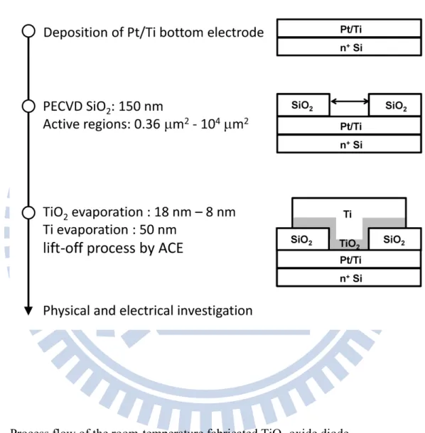
Fig. 2.1 Process flow of the room-temperature fabricated TiO2 oxide diode …………..32
Fig. 2.2 Capacitance measurement of Ti/TiO2/Pt MIM diode in the area of 104 m2. Inserts
show the XRD pattern and the TEM image of the as-deposited TiO2.……….…33
Fig. 2.3 XPS spectrum of the O 1s core level in TiO2 film. The signal of non-lattice
oxygen was eliminated by an additional 400 oC annealing in O2 ambient…….…34
Fig. 2.4 J-V characteristics of a typical Pt/TiO2/Ti MIM diode. The thickness of TiO2 is 8
nm. Insets show the band structures of the MIM under different biases and the Schottky-emission fitting of Ln J vs E1/2 from -1.4 to -4 V, respectively……...35 Fig. 2.5 Optical microscopy images of top-view Ti/TiO2/Pt diode. The thickness of TiO2 is
18 nm and the area of active region is 100 m × 100 m. Gas bubbles were induced by a series of voltage configurations from +5 V to +10 V………...36 Fig. 2.6 (a) SEM image after removing the Ti top electrode, (b) Surface morphology by
AFM and (c) surface conductivity by C-AFM on the specific position labeled in (a)………37 Fig. 2.7 J-V characteristics of Ti/TiO2/Pt MIM diodes with various device areas fabricated
by photolithography process. Current density of 104 A/cm2 at –3 V with device
area down to 0.36 m2 was obtained……….…...38
Fig. 2.8 Temperature-dependent Schottky-emission fitting of the Ti/TiO2/Pt MIM diode at
(a) forward and (b) reverse bias measured from 25 oC to 125 oC. Insets show the extracted Schottky barrier height as a function of applied voltage………39 Fig. 2.9 Endurance characteristics of the TiO2 MIM diode at (a) 25 oC and (b) 125 oC,
showing a stable operation more than 103 cycles under ±3V sweep. (c) 200 successive bipolar resistive-switching cycles after the forming at +5V. Inset shows the forming process with compliance current of 1 A………...40
Chapter 3
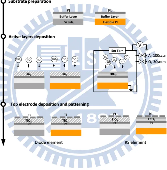
Fig. 3.1 Fabrication flow of Ti/TiO2/Pt, Pt/TiO2/Pt and Ni/HfO2/Pt devices on PI and Si
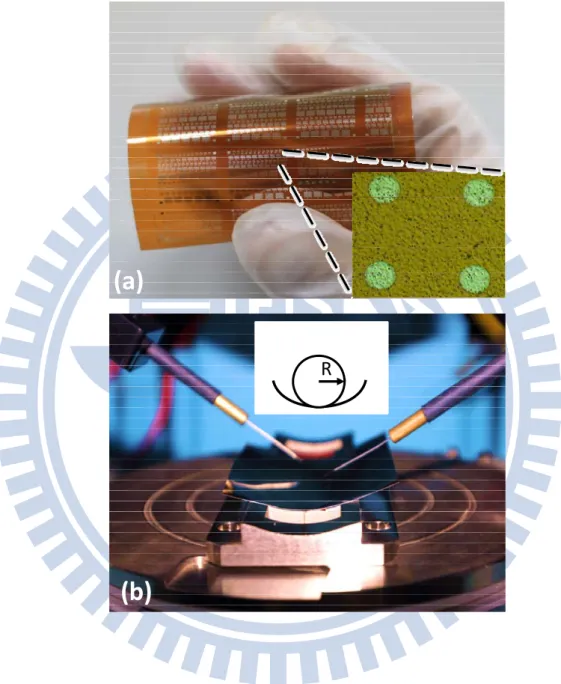
substrates……….………..………....48 Fig. 3.2 (a) Photograph of a fabricated flexible device under bending and insert shows the microscope image of patterned devices on the PI substrate. (b) Measurement setup using a concave stage with a radius of 30 mm to characterize devices at the bending state……….………..…...49 Fig. 3.3 (a) 100 successive cycling of ±2 V dc sweeps, and (b) cumulative plot of
forward/reverse resistances at +1V/-1V of the flexible Ti/TiO2/Pt diodes at both
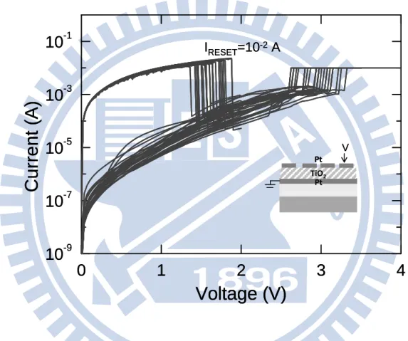
Fig. 3.4 Typical unipolar RS characteristics of the Pt/TiO2/Pt memory element with IRESET
over 10 mA……….51 Fig. 3.5 Unstable unipolar RS in the monolithic TiO2 1D1R cell because of the small
programming margin………..52 Fig. 3.6 (a) Programming margin of a 1D1R cell as a function of IRESET and the diode
on-current was fixed at 10 mA. A RHRS/RLRS ratio of 100, VRESET of 0.5 V and VSET
between 2 to 4 V considering cycling variations were assumed for the RS element. (b) Simulated 1D1R unipolar switching curves for RS elements with IRESET of 0.1
mA and 10 mA, respectively………..53 Fig. 3.7 (a) 100 successive unipolar RS cycles with IRESET less than 1 mA, and (b)
cumulative plot of HRS/LRS resistance at 0.2 V of the flexible Ni/HfO2/Pt
memory element at both flat and bending states………54 Fig. 3.8 Read disturb and retention characteristics of the flexible Ni/HfO2/Pt memory
element at both flat and bending states………...55 Fig. 3.9 More than 200 successive unipolar RS cycles with a high rectifying ratio at ±1 V
in the heterogonous TiO2-HfO2 1D1R cell……….56
Fig. 3.10 ( a ) T E M i m a g e a n d s c h e m a t i c s t r u c t u r e o f v e r t i c a l l y s t a c k e d Ti/TiO2/Pt/Ni/HfO2/Pt 1D1R cell and (b) unipolar RS I-V with a high rectifying
ratio of the vertically stacked 1D1R…….………...57 Fig. 3.11 Schematic of an N × N crossbar memory array and its equivalent circuit at the worse-case read scenario where all unselected cells are at LRS. The sneak current through R1, R2 and R3 results in severe read interference………...58
Fig. 3.12 Equivalent circuit of a 1D1R crossbar array at read. The total resistance of the sneak current path is dominant by R2 because of the reverse-biased diodes……..59
Fig. 3.13 Normalized readout margin V/Vpu as a function of the number of word/bit line in
an N × N crossbar array. The maximum allowed array size with at least 10 % readout margin can be dramatically increased in 1D1R arrays compared to 1R passive arrays………..60
Chapter 4
Fig. 4.1 Sneak current path at read in a square crossbar array where all bits except the selected one are at LRS, and (b) the equivalent circuit can be represented by RI, RII,
and RIII of parallel resistor networks in region 1 (bits on selected BL), region 2
(bits on unselected WL and BL), and region 3 (bits on selected WL).…………..69 Fig. 4.2 RS I-V curves for (a) 1D1R and (b) 1S1R RRAM cells, and their nonlinearity
factor and equivalent circuits in a crossbar array. RII subjected to a reverse bias
is much larger than RI and RIII in 1D1R, while RII scaled with (N-1)2 is much
smaller than RI and RIII scaled with (N-1) in 1S1R………70
Fig. 4.3 Calculated read margin as a function of for both 1D1R and 1S1R using the equivalent circuits in Fig. 4.1 and RHRS/RLRS = 103………...71
Fig. 4.4 (a) I–V characteristics of the bipolar Ni/TiO2/Ni MIM selector (S1) and bipolar
Ni/HfO2/Pt RS elements (R1 and R2), and (b)(c) TEM cross-section images of the
Ni/TiO2/Ni selector……….72
Fig. 4.5 (a) Endurance I-V of Ni/TiO2/Ni selector over 1000 cycles, (b) Schottky emission
fitting of log (I) versus V1/2 at both voltage polarities of S1 and (c) extracted Schottky barrier height Φb by temperature-dependent fitting from the low voltage
regime of S1………...………73 Fig. 4.6 I-V characteristics of Ni/TiO2/Ni bipolar selectors with various device areas
fabricated by conventional lithography on Si substrates. Insert shows that current density higher than 105 A/cm2 with device area scaling down to 0.36 m2 can be
achieved………..74 Fig. 4.7 (a) More than 200 successive bipolar switching cycles of S1 and R1 connected in series with 100 μA compliance current and (b) read disturbances for the HRS stressed at +3 V and the LRS stressed at –3 V………75 Fig. 4.8 Read margin V/Vpu as a function of N in various crossbar configurations
Chapter 5
Fig. 5.1 (a) Polyimide (PI) substrates were prepared and ultrasonically cleaned in acetone. (b) Pt/Ti bottom electrodes deposition through mask 1………..…...83 (c) HfO2 deposition through mask 2 and (d) Ni metal layer deposition through
mask 3………....84 (e) TiO2 deposition through mask 4 and. (f) Ni top electrode deposition through
mask 5………...…..85 Fig. 5.2 (a) Cross-sectional view and (b) photograph of a flexible 8×8 1S1R memory array with a curly bending, and (c) optical microscope image of a vertically stacked
Ni/TiO2/Ni/HfO2/Pt cell……….………....86
Fig. 5.3 Photograph of a flexible device with a bending radius of 10 mm under electrical testing……….87 Fig. 5.4 Highly nonlinear and reproducible I-V curves of Ni/TiO2/Ni bipolar selector (1000
successive cycles) by Schottky emission over Ni/TiO2 barriers………88
Fig. 5.5 (a) Endurance of flat and bending Ni/TiO2/Ni bipolar selectors under ±3 V DC
cycling and (b) measured resistance of Ni/TiO2/Ni bipolar selector at alternate flat
and bending states………...89 Fig. 5.6 (a) 100 successive bipolar RS I-V curves and (b) cumulative distribution of SET voltage and RESET voltage for both flat and bending Ni/HfO2/Pt memory
elements………..90 Fig. 5.7 (a) Read disturbance measurement stressed at 0.2 V and (b) retention
measurement of flat and bending Ni/HfO2/Pt memory elements……….…..91
Fig. 5.8 (a) Transient response of RS by a 100 ns pulse at ±4 V and (b) robust endurance of Ni/HfO2/Pt memory element under 106 cycles of ±4 V, 100 ns pulse
switching……….………92 Fig. 5.9 Bipolar I-V RS cycles of vertically stacked Ni/TiO2/Ni/HfO2/Pt with of 103 at
Vread of 1.2 V………...93
Fig. 5.10 Read margin between LRS and HRS in an 8 × 8 1R array and 1S1R array where all unselected bits were at LRS (See equivalent circuits in Fig. 4.1 & 4.2)...94 Fig. 5.11 (a) Vdd/2 SET/RESET scheme where only the unselected bits on the activated WL
and BL are subjected to disturb voltage of V/2 and (b) SET/RESET disturbance measurement at 1/2 VSET/VRESET on vertically stacked Ni/TiO2/Ni/HfO2/Pt. HRS
was stressed at +2 V while LRS was stressed at -2 V………95 Fig. 5.12 Comparison of the maximum allowed array number based on the reported 1S1R [77, 79], 1D1R [73] and CRS [41, 78] architectures…………..…..………..96
Chapter 1
Introduction
1.1 Background
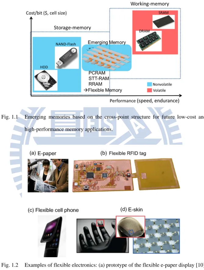
Metal-oxide semiconductor (MOS) transistor-based memories (such as Dynamic Random-Access Memory (DRAM) and NAND-flash memory) have played an important role for decades in the development of semiconductor industries. However, technologies scaling beyond 20 nm nodes are facing fundamental physical limits, and the increasing leakage power of DRAM has challenged the circuit and architecture concerns for future memory hierarchy designs [1-3]. One well-known limitation of NAND-flash is the time-consuming writing, which restricts its continuous scaling as a candidate for future memory technologies. Alternative memory technologies for factors, such as scalability, high-density, and writing speed, must be taken into consideration. Therefore, the best approach towards these goals is to use a two-terminal memory device with a stackable structure integrated into a crossbar geometry. Consequently, emerging memory technologies based on different concepts, including Phase Change RAM (PCRAM) [4], Spin Torque Transfer RAM (STT-RAM) [5], and Resistive Switching RAM (RRAM) [6], have been extensively explored in recent years, as shown in Fig. 1.1. Among these emerging memory technologies, the so-called RRAM memories, based on the electrically switchable resistance between at least two distinguishable states, are the most promising candidates. From the viewpoint of material choice, moreover, it is much easier to use CMOS process compatible materials. Therefore, only RRAM technologies are discussed in our study.
the development of “soft electronics” has attracted progressively attention because they are lightweight, portable, inexpensive, and human-friendly interfaces [7-9]. Recently, many researchers have explored various flexible electronic devices, such as e-paper [10], flexible Radio-frequency identification (RFID) tags [11], flexible cell phones [12], and e-skins [7], as shown in Fig. 1.2. These works demonstrated the feasibility of their applications to specific components in electronics. Among which, flexible memories are required in each flexible system, showing the critical role that flexible memories play in flexible technologies. If technologies and processes used to fabricate inflexible memory devices could be adopted by flexible substrates, memory technologies could be potentially transferred into flexible substrates. Thus, it is worthwhile to explore inflexible technologies that may have the potential to be used in flexible substrates. Because of its room-temperature process, RRAM is suitable for all oxide-based devices, making it possible to be implemented in flexible electronic applications.
In this chapter, we review the development of currently established RRAM technologies in Section 1.2. Starting from basic device architectures to integrated crossbar arrays, various selection devices proposed to suppress the sneak current is reviewed. Then, the operation methods of “write” and “read” in crossbar arrays are included in Section 1.2.3. Finally, the motivation of this dissertation and thesis organization are described in Sections 1.3 and 1.4, respectively.
1.2 Development of Resistive-Switching RAM (RRAM)
Resistive-switching (RS) behaviors in MIM structures have been explored since 1962 [13]. Accompanying a large variety of high- materials progressively used in CMOS technologies, the further prosperous development of RRAM was triggered by Waser et al. in 2007 [6]. The RS effects were observed in various material systems under electrical stress
but only the effects, such as electrochemical, valence change, and thermochemical-related are classified in the RRAM group [14]. In this section, we start to describe the basic concepts of RRAM cell and its related structure built in crossbar arrays. Material systems and physical mechanisms of RS phenomena are not discussed in this dissertation but are reviewed in other studies in our group [15, 16].
1.2.1 Basic concepts of RRAM
As shown in Fig. 1.3(a), a RRAM element is formed at the junction between the top and bottom metal layers. Each RRAM element can be interconnected to form a typical crossbar array with an electrode pitch of 2F, where F is the feature size of a technology node. Thus, a mini-RRAM unit cell with an ultrahigh density of 4F2 can be achieved. In this capacitor-like MIM structure, an insulating or switching layer (I) is sandwiched between two metal electrodes (M). By electrically stimulating the devices, RS properties were observed in various binary oxides, such as NiO [17], TiO2 [18], Ta2O5 [19], and HfO2 [20]. Among
which, HfO2 is particularly favorable material in present CMOS technologies.
Typically, an initial electroforming process accompanied by an appropriate compliance current must be introduced to activate the virgin RRAM device. Afterward, by applying either a voltage or a current to the RRAM device, RS processes from the high-resistance state (HRS) to low-resistance state (LRS) and from LRS to HRS are called SET and RESET, respectively, as shown in Fig. 1.3(b). These distinctive reproducible states (HRS/LRS) are able to retain their resistance levels for a quite long period, allowing information to be retrieved when a small read voltage (Vread) is applied. In principle, RS in RRAM can be
classified into two main switching schemes: unipolar RS and bipolar RS, which are usually identified by the polarity of voltage or current during operation. In unipolar switching, both SET and RESET operations occur on the same polarity, whereas in bipolar switching, it requires two polarities to finish one SET/RESET cycle.
1.2.2 Development of selection devices for crossbar RRAM
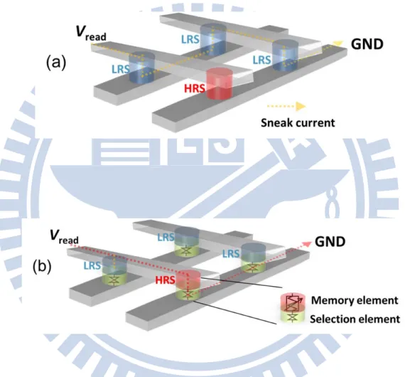
In the simplest case, RRAM cells are typically organized in a passive crossbar array. However, RRAM cells in passive crossbar arrays are inherently suffered from undesired sneak currents entering through the surrounding cells during the reading process. As shown in Fig. 1.4(a), a selected HRS cell surrounded by three neighboring LRS cells can easily pass sneak currents through the neighboring LRS cells. Consequently, the read interference may significantly deteriorate the read margin (ΔV/Vpu) and limit the maximum allowed size in a
crossbar array [21, 22]. It was reported that an inborn nonlinear I-V of LRS in a RS element can yield better results in an increased voltage swing (V) [21-23]. However, this approach limits the freedom of the design criteria of the RS element, and its low nonlinearity is insufficient to build M-bit or G-bit array sizes [22].
Therefore, finding additional selection devices with a specific degree of nonlinearity added at each node, where current flow is allowed only for the selected cell and suppressed for the unselected cells, is inevitably required (Fig. 1.4(c)). A selection device is required to have a high-current density, as well as important to the selectivity. The turn-on current density must be sufficiently high to meet the minimum current requirement for a successful switching at a given technology node without causing itself breakdown. For example, at the technology node of 100 nm, the current density of 105 A/cm2 provided by a selection device is needed for an Ireset of 10 A, as shown in Fig. 1.5 [24]. Depending on the switching
scheme of RRAM elements, several selection devices have been proposed, and are being considered promising solutions. The four possible configurations, shown in Table 1, One Transistor-One Resistor (1T1R or 1BJT1R), One Diode-One Resistor (1D1R), Complementary Resistive Switching (CRS), and One Selector-One Resistor (1S1R) in the operation scheme, and process complexity and feasibility are discussed in this subsection.
(a) One Transistor - One Resistor (1T1R)
A 1T1R cell organized by connecting a transistor and a resistor in an active matrix is shown in Fig. 1.6(a). Because of the transistor’s superior switch ratio, the 1T1R architecture can significantly reduce crosstalk and interference signals in crossbar arrays. A 1T1R was also introduced to control the filament size by preventing the overshoot current during the forming process [24]. This work shows that the controlled forming current allows a relatively large HRS and a subsequent reset current (IRESET) below 100 A (Fig. 1.6(b)), which
indicates a scalability of IRESET through an integrated transistor in the series with a RRAM. In
addition, it has been reported that the transient current through the parasitic capacitance of the MIM structure can be further reduced in the integrated 1T1R when the forming or the set process occurs [25]. However, 1T1R and 1BJT1R structures are not suitable for 3D stacked structures because of their high-temperature processes and additional area for transistor contact.
(b) One Diode - One Resistor (1D1R)
In the unipolar RS scheme, the sneak current can be resolved through a rectifying diode as a selection device. This stacked 1D1R structure capable of 4F2 crossbar array, without affecting storage density (Fig. 1.7(a)), is one of the most attractive candidates [26-29]. Considering various materials used in diodes, the types of diodes employed in the 1D1R cell mainly include Si-based diodes [27, 30] and oxide-based diodes [31-34]. However, epitaxial Si-based p-n diodes are not suitable for the stacking structure because of their high-temperature process, and they are problematic in epitaxy high-quality silicon on oxide layers.
Oxide-based diodes are powerful candidates to address these issues. Two oxide layers, one n-type oxide and one p-type oxide, were used to form a rectifying p-n oxide diode, as shown in Fig. 1.7(b) [31-33]. However, the proposed p-n oxide diodes with a high turn-on
voltage, too-high ideality factor, and insufficient Forward/Reverse (F/R) ratio still remain concerns; additionally, two thin oxide layers with specific compositions increase challenges in manufacturability. Another way to approach the rectifying behavior is to modulate the Schottky barrier at the metal/oxide interfaces during fabrication [18, 35, 36], or to choose applicable top and bottom metal electrodes in MIM structures [37, 38]. These Schottky-type diodes, fabricated in a relatively simple process, are capable of achieving a local forward current density of approximate 104 A/cm2 (will discuss in Chapter 2) and a high F/R ratio at a relatively-low voltage, which are crucial merits of this type of diode. When a diode was integrated with a RS element, the well-behaved switching and the significant rectification could be achieved, as shown in Fig. 1.7(c).
In addition, the current density of the forward-bias diodes is an important factor that may limit the scaling, as shown in Fig. 1.5. To further improve the current density for a compatible IRESET is necessary to allow a reliable unipolar RS.
(c) Complementary Resistive Switching (CRS)
CRS, consisting of two antiserially bipolar RS elements, has been proposed as a possible solution for bipolar RRAM to suppress the sneak current [39]. As shown in Fig. 1.8(a), elements A and B are merged to form one CRS cell, where a superimposed I–V characteristic can be directly obtained. In contrast to the concept of passive crossbar arrays, the overall resistance of a CRS at Vread/2, regardless of the “1” or “0” stored, is dominated by
the large HRS on either element A or element B. Basically, the CRS acts by essentially the same principle as a CMOS inverter, in which one of the transistors is always OFF. To read the resistance state of CRS, Vread between Vth,1 and Vth,2, or Vth,3 and Vth,4, was chosen to read
the selected cell. At this point, if an ON-state exists in the CRS, a significant current will be detected. Several studies have experimentally demonstrated the feasibility of CRS cell [40,
I-V curve in accordance with the predicted operation scheme. But, a critical trade-off in CRS
between the read voltage window and the write voltage window must be carefully designed [42].
Furthermore, the inherently destructive reading of CRS imposes severe penalties on the design complexity, writing speed, and power consumption. In addition, a stable bipolar switching for both RS elements is also a concern to obtain reliable read/write endurances.
(d) One Selector - One Resistor (1S1R)
By considering an additional selection device, the commonly used rectifying diodes are not suitable for a bipolar RRAM because it needs two polarities to complete one SET/RESET cycle. In other words, the selection device must have a bidirectional and nonlinear I-V to allow the bipolar switching. Fig. 1.9(a) shows the I-V characteristics of a bipolar RRAM with and without a bipolar selector. When using the one bit-line pull-up read scheme (One-BLPU) to evaluate the read process, as shown, the sneak current at Vread/2 of
the unselected cells was apparently eliminated, indicating a possible solution to reduce the sneak current. A so-called Zener diode was applied to this configuration. As in a regular diode, it allows current to travel in both forward and reverse directions if the voltage was larger than the reverse Zener voltage. However, like the traditional Si-based diode, the complex and high-temperature process makes Zener diode unsuitable for the stacking memory process. In addition, it has difficulty obtaining a reasonable Zener voltage to match the low-power requirement of a bipolar RRAM. Recently, a voltage-controlled varistor based on the low-temperature oxide materials, with bidirectional and symmetrical I-V characteristics, has been proposed [43, 44]. Cell structures composed of one nonlinear bipolar selector and one bipolar RS element (1S1R) can best use the stable bipolar RS properties. In contrast to modulating the inborn nonlinearity of RRAM, the nonlinearity of 1S1R at a small voltage can be separately controlled by the selector. In Fig. 1.9(b), the sneak
current of LRS at Vread/2 can be significantly blocked by the proposed 1S1R cell as compared
to a selector-less bipolar RRAM. So far, the endurance of 1S1R cell has not yet been verified because the selector may suffer dielectric breakdown at high voltage. Additionally, the reported bipolar selector had limited nonlinearity sufficient only for a small 8 × 8 array [43]. Based on above reasons, the improved 1S1R characteristics and the flexible 1S1R array will be discussed in Chapters 4 and 5,
1.2.3 Operation methods of crossbar RRAM
The performance of write to and read from passive crossbar arrays can be improved by connecting a suitable selection device, such as diodes or bipolar selectors, but still challenged. For write to crossbar arrays, a selection device must be able to write the selected cell without inferring the unselected cells. During a read operation, on the other hand, a logical “0” must be distinguishable from a logical “1” on the selected cell and vice versa. Therefore, both read and write operations must minimize the disturbance of unselected cells, and maximize power efficiency simultaneously.
(a) “Write” operation
When a memory cell is selected to perform a write operation, the other unselected cells connected to the unselected WLs/BLs are simultaneously subjected to a certain part of bias voltage. Ideally, a desired write operation should have high bias voltage to the selected cell and avoid disturbing the unselected cells. To bias the unselected WLs/BLs, there are two famous biased schemes, which are the Vdd/2 scheme, where the unselected cells are biased to
voltages of either V/2 or 0; and the Vdd/3 scheme, where all the unselected cells are biased to
voltages of either V/3 or –V/3 [45].
half-voltage (V/2) is applied as schematically shown in Fig. 1.10(a). Consequently, the selected cell is under a forward bias of V and the other unselected cells are biased to either
V/2 or 0. On the other hand, in the Vdd/3 scheme shown in Fig. 1.10(b), the selected cell is
biased to a voltage drop (V) as in the case of Vdd/2 scheme. In contrast to the Vdd/2 scheme,
the unselected WLs and BLs are subjected to bias voltages of one-third of V (V/3) and two-thirds of V (2V/3), respectively. In this scheme, the selected cell is under a forward bias of V and the other cells on the unselected WLs/BLs are under voltages of V/3 or –V/3, implying that the disturb voltage is less-severe as compared to the Vdd/2 scheme. Only
one-third of VSET (VSET/3) can drop on the unselected cells, which has less probability of
causing erroneous RESET if a voltage VSET is applied to the selected cell. Therefore, the
stability of diodes under reverse bias is also a significant concern to avoid –VSET/3 not
causing the breakdown.
(b) “Read” Operation
The read operation is of particular concern in RRAM because the read process depends strongly on the stored pattern in the crossbar array, which may restrain the maximum array size. To analyze this process, a simplified n × m crossbar array is schematically depicted in Fig. 1. 11(a). The read operation is performed by applying a pull-up voltage (Vpu) to the
selected BL and the selected WL is grounded. A convenient way of designing an output voltage swing (Vout) with respect to the stored pattern is by introducing a pull-up resistor
(Rpu) parallely connected to the sensing amplifier (SA) on each BL. The Rpu value was
particularly designed to achieve the maximum Vout. In general, a sensing criterion of at least
10% read margin (ΔVout/Vpu) was chosen to determine the maximum available array size
[39].
In the worst-case scenario, the read margin was measured at the condition where the selected cell is on the corner of the array. In this pattern, one can divide the unselected cells
into three groups: Region 1 (cells on the selected WL), Region 2 (cells on the unselected WL and BL), and Region 3 (cells on the selected BL), as shown in Fig. 1.11(b). The line resistances of interconnects were ignored under this assumption. To read information from the crossbar array, there are generally three ways to bias the unselected WLs/BLs: by Vdd,
grounding, or floating, which contributes nine possible configurations, as shown in Fig. 1.12 [46]. The voltage configurations in the crossbar array play a crucial role in sensing margin, disturbance, and power efficiency. Specifically, Vout is significantly influenced by the
random resistance patterns as well the configurations, giving the indistinguishable sensing margin. In addition to the sensing margin, although the parallel leakage paths (shown by dashed lines) do not affect the voltage swing, an obvious power waste is raised.
The simplest read operation is configuration 1, the so-called One-BLPU. In this configuration, only the selected WL/BL is biased, and all the unselected WLs/BLs are left floating. When multiple or all bit lines are biased, they are referred to partial or all bit-line pull-up schemes (All-BLPU). To examine the performance of selection devices applied in crossbar arrays, it is much easier to choose the simplest read configuration (configuration 1) for our study.
1.3 Motivation
Flexible electronics have attracted much attention because of their advantages of simplicity, foldability and low manufacturing costs over conventional Si-based technologies [9, 11]. One critical concern of flexible electronics is to implement inflexible nonvolatile memories into flexible nonvolatile memories. Crossbar RRAM has been considered to be best solution in flexible memories. However, the reported flexible memories, consisting of only a few memory elements in the passive crossbar array, are not enough to provide a breakthrough evidence for flexible memory applications [47-49]. Furthermore, it is an
important project not only to further improve the switching reliability of RRAM cells, but also to find a suitable selection device to suppress the sneak current. Although traditional Si-based transistors have been the best solutions for DRAM and NAND-flash arrays, a high-temperature fabrication process and a cell size of at least 6F2 confine their continuous utilization in the crossbar RRAM [31]. In addition, CRS suffers from the issue of destructive read, which also increases the complexity of circuit design. Hence, 1D1R and 1S1R architectures appear to be the leading contenders for crossbar RRAM applications. Based on the present RRAM technologies, various oxide-based diodes have been explored in unipolar 1D1R architectures, but low rectification ratios and insufficient current densities are unable to achieve a reliable switching.
This dissertation employs TiO2-based selection devices on flexible substrates by simple
and room-temperature processes. To prove a fully oxide-based functional flexible memory, and prevent an undesired sneak current, each memory cell was integrated with a selection component. Based on the switching polarities, a unipolar Ti/TiO2/Pt diode with a unipolar
RS element and a bipolar Ni/TiO2/Ni selector with a bipolar RS element were fabricated to
construct a 1D1R and a 1S1R architectures, respectively. Endurance characteristics of 1D1R unipolar and 1S1R bipolar switching were also investigated. The top and bottom metal lines of 1S1R cells were further interconnected to construct an 8 × 8 crossbar array on a flexible substrate to examine the rad margin.
The goal of this study is to find low-temperature process available selection devices and demonstrate their roles in suppressing sneak currents, especially for their implementations on plastic substrates. These results can assist designers in writing new guidelines for realizing a fully-oxidized crossbar RRAM for high-performance flexible memories.
In this thesis, a TiO2-based material through a simple process to construct flexible
selection devices is proposed. The well-behaved Ti/TiO2/Pt diode shows superior 1D1R
switching characteristics by externally connecting a HfO2-based memory element. Nonlinear
Ni/TiO2/Ni bipolar selectors were investigated using the stable bipolar 1S1R switching. This
study also highlights the scaling potentials of 1D1R and 1S1R in future RRAM technology from the viewpoint of nonlinearity using a One-BLPU read scheme. Finally, an 8 × 8 1S1R array on flexible substrates was successfully realized. This dissertation contains four main concepts, which are organized into six chapters, as follows:
In Chapter 1, the development of currently established RRAM technologies are reviewed, starting from the device cell to the integrated crossbar array. Various selection devices based on the switching polarities to suppress the sneak current are discussed. The operation methods of crossbar RRAM are also described.
In Chapter 2, the stable rectifying and resistive-switching properties of a Ti/TiO2/Pt
MIM structure are investigated. Oxygen migration and localized conductive filaments play important roles in the resistive switching of RRAM and the rectification of oxide diodes. After forming at higher voltages, significantly stronger filaments destroying the interface Schottky barrier denotes reproducible resistive switching. Moreover, the current density of TiO2 MIM diodes at –3 V more than 104 A/cm2 can be achieved, showing satisfactory
requirements in TiO2 MIM diodes for future 1D1R RRAM applications.
In Chapter 3, a rectifying Ti/TiO2/Pt oxide diode and a unipolar RS Ni/HfO2/Pt memory
element were fabricated on a flexible PI substrate with excellent characteristics using only room-temperature processes. No significant device degradations are found under the bending states. Additionally, the impact of IRESET on the programming margin of unipolar RS has been
discussed. The heterogeneous TiO2-HfO2 1D1R cell not only shows more sreliable unipolar
predicted to be able to build 512 Kb memory size based on a simple equivalent circuit model.
In Chapter 4, a Ni/TiO2/Ni MIM with highly nonlinear I-V characteristics was used as
the bipolar selector for high-density 1S1R crossbar arrays. The nonlinear I-V is attributed to the Schottky barriers at the Ni/TiO2 interfaces. When the selector element was further
connected with the HfO2 RS element, the combined 1S1R cell exhibits a robust and reliable
bipolar switching, and can effectively suppress the sneak current. In addition, 1D1R and 1S1R crossbar arrays are compared in this chapter. These results demonstrate the promising potential of the 1S1R crossbar array for future high-density memory and reconfigurable logic circuit applications.
Chapter 5 shows a high-performance 8 × 8 1S1R crossbar array on plastic substrates realized by a simple and low-temperature fabrication process. The flexible Ni/TiO2/Ni and
Ni/HfO2/Pt elements also had excellent mechanical stability upon harsh bending.
Furthermore, the vertically stacked 8 × 8 1S1R array with superior read margin and immunity to disturb has been demonstrated, showing the potential application of future extremely low-cost flexible nonvolatile memories.
Finally, Chapter 6 states the conclusion as well as the recommendation for further research is addressed in this chapter.
Fig. 1.1 Emerging memories based on the cross-point structure for future low-cost and high-performance memory applications.
Fig. 1.2 Examples of flexible electronics: (a) prototype of the flexible e-paper display [10], (b) photograph image of the flexible circuit and the flexible antenna [11], (c) a bendable cell phone [12] and (d) stretchable electronics with a mesh design wrapped onto a model of a fingertip [7].
Fig. 1.3 (a) Schematic diagram of a crossbar RRAM, consisting of each memory element sandwiched between top and bottom electrodes with an electrode pitch of 2F, and (b) I-V switching curves of unipolar switching (left) and bipolar switching (right).
Fig. 1.4 Schematic diagrams of a crossbar structure: (a) without selection elements, where the sneak current through surrounding cells during a reading process and (b) with selection elements to cut off the sneak current through LRS cell.
Fig. 1.5 Calculated minimum current requirement of IRESET as a function of technology
node F, in which current density of 105 A/cm2 is required for IRESET of 10 A at
Fig. 1.6 (a) Circuit configuration of a 1T1R cell and (b) the measured SET/RESET characteristics for 1T1R devices, where a higher VG was used for RESET process
and a lower VG for SET process [24].
Fig. 1.7 (a) Schematic structure of a 1D1R crossbar array and its typical I-V switching curve, and (b) 1D1R I-V characteristics of the combined RRAM element and p-oxide/n-oxide diode [31] and (c) the series connected Pt/TiOx/Pt/TiOx/Pt device
Fig. 1.8 (a) Schematic concepts of Complementary Resistive Switches (CRS) and their representative CRS I-V curves [39], and (b) the measured CRS I-V characteristics of an anti-serial connected Pt/ZrOx/HfOx/BE/HfOx/ZrOx/Pt stacking structure
Fig. 1.9 Comparison of Vdd/2 reading characteristics of a bipolar RRAM without and with
a selector and (b) the measured bipolar 1S1R I-V curve of externally connected Pt/TiO2−x/TiO2/W and Pt/TiO2/TiN device [43].
Fig. 1.10 Schematic of the Vdd/2 and (b) Vdd/3 SET/RESET scheme. Only the selected cells
Fig. 1.11 Circuit diagram of an n × m crossbar array and (b) its corresponding equivalent circuit when Vread was applied at the corner of the crossbar array.
Fig. 1.12 Summary of possible voltage configurations and their equivalent circuits during read operation [46].
Chapter 2
Stable Rectification to Resistive-Switching in
Ti/TiO
2/Pt MIM Diode
2.1 Introduction
RRAM consists of simply a layer of TMO sandwiched between two metal electrodes, ideal for high-density 4F2 cross-point memory array. However, read and write disturbance due to the sneak current among neighboring cells is a serious concern in RRAM where the memory states are partially determined by the cell resistance of the sneak path [21, 22]. The unit cell of RRAM inevitably requires an extra transistor or diode to alleviate the problem of disturbance. The one transistor-one resistor (1T1R) cell best leverages the maturity of transistor technology. Nevertheless, it is unfavorable to high-density memory array where the size of unit cell and the low-temperature three-dimensional (3D) stacking is of the interest. On the other hand, the one diode-one resistor (1D1R) cell where oxide diodes with high forward current are utilized possesses compact cell structure and low thermal budget. It holds particular promise for future high-density stackable nonvolatile memory applications [26, 31].
The metal/insulator/metal (MIM) and metal/insulator/insulator/metal (MIIM) structures are among popular implementations of high-current oxide diodes. In MIIM, the rectifying p-n junction is formed by two different oxide layers, one n-type oxide and one p-type oxide. High current density and sufficient ON/OFF ratio have been reported but the high turn-on voltage and ideality factor are less than ideal [31, 50]. The requirement of two thin oxide layers with specific composition also poses challenges in manufacturability. In MIM, the rectifying Schottky junction is formed at the metal/oxide interface. Well-behaved diode
characteristics applicable for the 1D1R RRAM have been achieved [37, 51]. Moreover, most TMOs used in MIM diodes also show pronounced resistive switching properties. For example, Shima et al. [35] have reported the rectifying and resistive-switching behavior in a Pt/TiOx/Pt MIM. However, the study on the transition and controllability between the resistive-switching and the rectification has been largely overlooked in the literature but critical to guarantee stable operation in the 1D1R.
Therefore, in this chapter we fabricated a high-forward-current Ti/TiO2/Pt MIM diode
at room temperature by a very simple evaporation process. Excellent rectifying characteristics including a rectifying ratio of 105 at ± 3 V, a forward current density of 2×10³ A/cm2, an ideality factor of 1.2, and a turn-on voltage of 0.5V are estimated. We also show that the conduction through the interface of Schottky barrier is inhomogeneous in nature because of the localized oxygen migration. We can therefore furthermore identify the evidence of high current density of TiO2 diode is due to the local current conduction. In
addition, TiO2 has been known for its excellent resistive-switching properties [18, 53]. Here,
we demonstrate the coexistence of diode rectification and bipolar resistive-switching in the identical TiO2 MIM structure by controlling the electrical forming process. Both operation
modes are stable without interference with each other up to 125oC. The physical origins of resistive-switching to rectification are also included in this work.
2.2 Experimental Procedure
Pt bottom electrodes of 80nm with a thin Ti adhesion layer were deposited onto heavily doped n-type Si wafers by electron beam evaporation. After SiO2 deposition by
plasma-enhanced chemical vapor deposition (PECVD), contact-hole structures with size of 0.36 m2 to 104m2 were defined by photolithography and SiO
2 dry etching. TiO2 with
granules (Admat Midas Inc., 99.9 wt% purity) as the source at room temperature. Finally, Ti top electrodes of 80 nm were deposited by electron beam evaporation and lift-off process. The detailed process flow and device structures are illustrated in Fig. 2.1. The as-deposited TiO2 appeared amorphous can be examined from the X-ray Diffraction (XRD) as shown in
Fig. 2.2, where no crystalline signal was detected except the signal of Pt bottom electrode. The estimated dielectric constant () was around 18.5 from inspections of cross-section TEM and capacitance measurement. In Fig. 2.3, X-ray Photoelectron Spectroscopy (XPS) revealed considerable non-lattice oxygen in TiO2 layer, indicating substantial deficient oxygen existed
in the as-deposited TiO2 film. After an additional 400oC annealing in O2 ambient, the binding
energy of oxygen peaked at 531 eV and the broaden tail from the non-lattice oxygen vanished. All electrical measurements were carried out by applying voltage on the Ti top electrode while the Si substrate was grounded.
2.3 Results and Discussion
2.3.1 Current-voltage characteristics of Ti/TiO
2/Pt diode
Figure 2.4 illustrates the rectifying characteristics of the Ti/TiO2/Pt MIM diode. The
asymmetry of current density-voltage (J-V) curves is the consequence of different Schottky barrier heights at the Ti/TiO2 and the TiO2/Pt interfaces. When a positive voltage applies on
Ti, electrons inject from Pt to TiO2 and experience a substantial Schottky barrier. On the
other hand, when applying a negative voltage on Ti, electrons inject from Ti to TiO2 and
first experience the diode build-in potential owing to the metal work function difference between Ti and Pt. As the negative voltage increases, the current increases exponentially by modulating the potential barrier of the injected electrons. Finally, the forward current is limited by the smaller barrier at the Ti/TiO2 interface. The current dependence on the
emission is the dominant transport mechanism at high forward bias. Furthermore, we found the first I-V sweep of the diode is distinctly different from the rest of sequential sweeps. The turn-on voltage was lowered by 0.7 V with an improved ideality factor of 1.2. While the reverse current increases about one order of magnitude, the forward-bias current at voltage of −2 V remains the same. The turn-on voltage in the Ti/TiO2/Pt MIM diode is controlled by
the build-in potential while the reverse and forward currents are governed by the Schottky barriers at the TiO2/Pt and Ti/TiO2 interfaces, respectively. The discussion of Schottky
barrier at the TiO2/Pt interface modulated by the first I-V sweep will be evaluated in next
section, strongly supported by the evidences of physical observation.
2.3.2 Physical characteristics of Ti/TiO
2/Pt diode
Figure 2.5 shows a series of snapshots of visible bubbles, as different voltages were applied, observed by the optical microscope. After the voltage sweeps from 0 to +3 V, oxygen bubbles appeared and randomly distributed in the active region. This is attributed to the migration of oxygen ions triggered by the external voltage and thus accumulating beneath the top electrode (Fig. 2.5(b)) [53]. After the external voltage was removed, a much bigger bubbles were formed, which was originated from the migration and combination of neighboring bubbles, as shown in Fig. 2.5(c). With a relatively-large voltage (e.g. +10 V) was applied, a ruin region (permanent breakdown) was observed as indicated by the arrow in Fig. 2.5 (d). The physical deformation of the top electrode was attributed to the drift of oxygen ions in TiO2 toward the anode where they evolve O2 gas. Similar bubble formation
was previously reported in a Pt/TiO2/Pt RRAM cell [18]. The degree of bubble formation
depends strongly on the thickness of TiO2 and the polarity of applied voltage. Therefore, 18
nm TiO2 instead of 8 nm TiO2 was utilized for the physical characterization in this section.
film is negligible. The scanning electron microscope (SEM) image in Fig. 2.6(a) reveals scattered surface residues, which are lacking in the virgin samples without the bubble formation. The atomic force microscope (AFM) and the conductive AFM (C-AFM) in Figs. 2.6(b) and 2.6(c) further evidence these residual regions are the local current paths (filaments). This is attributed to the negatively charged oxygen ions that drift towards the anode under the positive bias and become oxygen-deficient at the Ti/TiO2 interface. The
defects at the TiO2/Pt interface may cause substantial Fermi-level pinning that shifts the Pt
workfunction upward and reduces the Schottky barrier at the TiO2/Pt interface [37]. As a
result, lower turn-on voltage and higher reverse-bias current are expected with oxygen-deficient TiO2. The oxygen piling up at the anode may react with Ti top electrode to
form TiOx, which is insoluble in dilute sulfuric acid and results in the observed residues.
Moreover, because the migration of oxygen ions is not homogeneous, the diode current is the superposition of the components through the conduction channel with oxygen-deficient TiO2 and through the rest of intact TiO2. The prior dominates at the low voltage regime
while the latter becomes more important and eventually prevails at the high voltage regime owing to its larger area within the device. In Fig. 2.7, higher current density with smaller contact-hole size patterned by photolithography can be directly observed, showing another evidence of inhomogeneous conduction in the Ti/TiO2/Pt diode.
2.3.3 Conduction mechanism
Figure 2.8 shows the temperature-dependent Schottky fitting of the Ti/TiO2/Pt MIM
diode measured from 25 to 125°C. The extracted barrier height at the TiO2/Pt interface is
estimated 0.73 eV by extrapolating to V=0. The smaller than expected barrier height is the result of the Fermi-level pinning phenomenon. The extracted barrier height at the Ti/TiO2
interface is estimated 0.13 eV at V= −0.85 V, which eventually limits the maximum forward-current density. J= 104 A/cm2 at |3V| reported here is comparable with other
TiO2-based MIM diodes [35, 37]. Future optimization to reduce the interface barrier will be
the key factor to increase the current density. Note that in comparison with the Pt/TiOx/Pt
MIM, where the rectification is achieved by the asymmetrical oxygen composition in TiOx
[35], the Ti/TiO2/Pt MIM not only shows improved rectifying characteristics but also
requires less complexity in fabrication.
2.3.4 Rectifying mode to resistive-switching mode
Figures 2.9(a) and (b) illustrate the stable rectifying characteristics of the MIM diode at 25 and 125 °C up to at least a thousand cycles under ±3 V sweep. The ON/OFF ratio keeps at least three orders of magnitudes even at 125 °C, and the forward-current density remains larger than 6×10² A/cm2 at 25 °C. A separate measurement also confirms no significant degradation of the diode characteristics under a constant 3 V stress up to 1000 s at 25 °C. In considering a practical 1D1R RRAM cell with SET/RESET pulse width of 100 ns, the result guarantees stable operation at least 1010 times. In Figs. 2.9(a) and (b), both forward and reverse current are reduced gradually after repeated cycling, especially at high temperature. The exact cause is still under investigation. One plausible explanation is that the bulk defects in TiO2 generated under stress deviate the current transport from the simple
Schottky emission. In addition, the Ti/TiO2/Pt MIM may switch from the rectifying mode to
the resistive-switching mode by applying a voltage larger than the soft-breakdown (forming) voltage around +5 V and appropriate current compliance. Figure 2.9(c) shows the reproducible bipolar resistive-switching with very tight distribution on SET/RESET voltages and high/low resistances. At the low voltage regime of the rectifying mode, the current transport is limited by the Schottky emission in local filaments. After forming, much stronger filaments across the entire thickness of TiO2 are developed by oxygen migration
controlling the forming process is critical to ensure no interference between rectification and resistive-switching. According to the popular E-model for oxide breakdown [56], the time to breakdown tBD is expressed as follows:
where A is a constant, is the field acceleration factor, Eox is the oxide field, Ea is the thermal
activation energy for oxide breakdown, kB is the Boltzmann constant, and T is the absolute
temperature. The experimental value of Ea for TiO2 in the literature is 0.5–0.7 eV [56].
increases with the dielectric constant in the thermochemical model for oxide breakdown [57]. Therefore, for our TiO2 (k=18.5) should be close to 13.6 MV/cm reported for Ta2O5 (k= 26)
[57]. Reasonable Ea and high in TiO2 enable the stable diode rectification at ±3 V without
triggering the forming in our interested time span even at 125 ° C.
2.4 Summary
In this study, we report the transition of stable rectification and resistive-switching properties in a Ti/TiO2/Pt MIM. The oxygen migration and localized conductive filaments
play important roles in not only the resistive-switching of RRAM but also the rectification of oxide diodes. When the current conduction through the oxygen-deficient TiO2 filaments
is limited by the interface Schottky barriers, the diode rectification prevails. After forming at higher voltage, much stronger filaments destroying the interface Schottky barrier give rise to the reproducible resistive-switching. The rectification properties are stable up to 125 °C and 103 cycles under ±3 V sweep without interference with resistive-switching. Moreover, the current density of TiO2 MIM diodes more than 104 A/cm2 can be achieved,
showing satisfactory requirement of TiO2 MIM diodes for future 1D1R RRAM
applications. exp( ) exp( a ) BD ox B E t A E k T
(Eq. 1.1)Fig. 2.2 Capacitance measurement of Ti/TiO2/Pt MIM diode in the area of 104 m2. Inserts
Binding energy (eV)
528
530
532
534
536
538
Intensity (a.u.)
Lattice oxygenO 1s
Non‐lattice oxygen TiO2after annealing As‐deposited TiO2Fig. 2.3 XPS spectrum of the O 1s core level in TiO2 film. The signal of non-lattice oxygen in
Fig. 2.4 J-V characteristics of a typical Pt/TiO2/Ti MIM diode. The thickness of TiO2 is 8 nm.
Insets show the band structures of the MIM under different biases and the Schottky-emission fitting of Ln J vs E1/2 from -1.4 to -4 V, respectively.
Fig. 2.5 Optical microscopy images of top-view Ti/TiO2/Pt diode. The thickness of TiO2 is 18
nm and the area of active region is 100 m × 100 m. Gas bubbles were induced by a series of voltage configurations from +3 V to +10 V.
Fig. 2.6 (a) SEM image after removing the Ti top electrode, (b) Surface morphology by AFM and (c) surface conductivity by C-AFM on the specific position labeled in (a).
Fig. 2.7 J-V characteristics of Ti/TiO2/Pt MIM diodes with various device areas fabricated by
photolithography process. Current density of 104 A/cm2 at –3 V with device area down to 0.36 m2 was obtained.
Fig. 2.8 Temperature-dependent Schottky-emission fitting of the Ti/TiO2/Pt MIM diode at (a)
forward and (b) reverse bias measured from 25 oC to 125 oC. Insets show the extracted Schottky barrier heights as a function of applied voltages.
Fig. 2.9 Endurance characteristics of the TiO2 MIM diode at (a) 25 oC and (b) 125 oC, showing a
stable operation more than 103 cycles under ±3V sweep. (c) 200 successive bipolar resistive-switching cycles after the forming at +5V. Inset shows the forming process with compliance current of 1 A.
![Fig. 1.8 (a) Schematic concepts of Complementary Resistive Switches (CRS) and their representative CRS I-V curves [39], and (b) the measured CRS I-V characteristics of an anti-serial connected Pt/ZrO x /HfO x /BE/HfO x /ZrO x /Pt stacking structure](https://thumb-ap.123doks.com/thumbv2/9libinfo/8472304.183587/38.892.168.742.119.999/schematic-complementary-resistive-switches-representative-characteristics-connected-structure.webp)
![Fig. 1.9 Comparison of V dd /2 reading characteristics of a bipolar RRAM without and with a selector and (b) the measured bipolar 1S1R I-V curve of externally connected Pt/TiO 2 − x /TiO 2 /W and Pt/TiO 2 /TiN device [43]](https://thumb-ap.123doks.com/thumbv2/9libinfo/8472304.183587/39.892.153.810.294.909/comparison-reading-characteristics-bipolar-selector-measured-externally-connected.webp)
![Fig. 1.12 Summary of possible voltage configurations and their equivalent circuits during read operation [46]](https://thumb-ap.123doks.com/thumbv2/9libinfo/8472304.183587/42.892.165.784.267.896/fig-summary-possible-voltage-configurations-equivalent-circuits-operation.webp)